Table of Contents
Advertisement
Quick Links
SERVICE
PLASMA DISPLAY TV
PLASMA DISPLAY TV
Chassis : D75A(N_50HD)_Cadillac
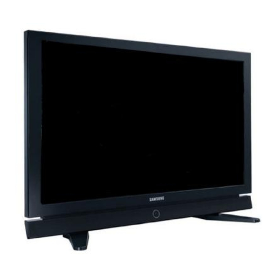
Model
: HPS5033X/XAA
Manual
■
■
■ 13-Bit Processing (549 Billion Colors)
■
■
■ Samsung DNIe™
■ SRS TruSurround XT™
■ 2 HDMI Input
■
■
■ SAMSUNG EPG System
HP-S5033
FEATURES
NTSC/ATSC Tuner Built-In
Split Screen & Picture-In-Picture
™
(Digital Natural Image engine)
™
Energy Saving
Advertisement
Table of Contents
Troubleshooting

Subscribe to Our Youtube Channel
Related Manuals for Samsung HPS5033X


Summary of Contents for Samsung HPS5033X
- Page 1 ■ ■ ■ 13-Bit Processing (549 Billion Colors) Split Screen & Picture-In-Picture ■ ■ ■ Samsung DNIe™ ™ (Digital Natural Image engine) ■ SRS TruSurround XT™ ™ ■ 2 HDMI Input Energy Saving ■ ■ ■ SAMSUNG EPG System HP-S5033...
- Page 2 © Samsung Electronics Co., Ltd. Jun. 2006 This Service Manual is a property of Samsung Electronics Co.,Ltd. Printed in Korea Any unauthorized use of Manual can be punished under applicable AA82-03790A International and/or domestic law.
-
Page 3: Table Of Contents
■ 5-1 HPS5033X/XAA Service Item ........ - Page 4 Chapter 9 PCB Diagram ■ 9-1 Main Board ..............9-1 ■...
- Page 5 Chapter 13 Circuit Description ■ 13-1 Power ON/OFF Signal Timing Sequence ......... 13-1 ■...
-
Page 6: Chapter 1 Precaution
When Check the AC power cord for possible damages. Keep voltage exceeds the specified limits, check each special the part or the lead away from any heat-emitting part. materials. Samsung Electronics... - Page 7 Critical safety parts should be bracketed with ( Use only regular parts for replacements (in particular, flame resistance and dielectric strength specifications). Irregular parts or materials may cause electric shock or fire. Samsung Electronics...
-
Page 8: Servicing Precautions
AC source and turn the switch on. Connect the insu- lating resistance meter (500v) to the AC plug blade. The insulating resistance between the blade of the AC plug and that of the conductive material should be more than 1 ㏁. Samsung Electronics... -
Page 9: Static Electricity Precautions
These servicing instructions are for use by qualified service personnel only. To reduce the risk of electric shock do not perform any servicing other than that contained in the operating instructions unless you are qualified to do so. Samsung Electronics... -
Page 10: Installation Precautions
5. Make sure to turn the power off and unplug the power cord from the outlet before repositioning the product. Also check the antenna cable or the external connectors if they are fully unplugged. Damage to the cord may cause fire or electric shock. Samsung Electronics... - Page 11 MEMO Samsung Electronics...
-
Page 12: Chapter 2 Product Specification
2-1 Product Features Block Specfication Major IC Remark VSB NIM Tuner Digital/Analog (DTV Built In) S5H2111X01(Lake) PDP Module Samsung SDI V5.1 Module 50" HD New Module Power Sanken Electric Co. SMPS 50" HD SMPS New SMPS NTSC 3.58, ATSC HDMI... -
Page 13: Key Features
COMPONENT1 - 480i/480p/720p/1080i AUDIO input COMPONENT2 - 480i/480p/720p/1080i AV Output AUDIO (L/R) Speaker Output 10W + 10W (8Ω ) OPTICAL(DIGITALOUT) Audio Output COAXIAL(DIGITALOUT) DNIe (LBE), Anynet, Color Weakness, SRS TruSurround XT, Dolby Digital, Built-in Speaker/Stand New Function Energy Saving Samsung Electronics... - Page 14 - 2 Component Inputs - 15 Pin PC D-sub Input - 2 HDMI Input - 2 SPDIF Output (Optical, Coaxial) - 2 RF Input : Cable/Air - 2 AV Inputs - 2 S-Video Inputs ■ Remocon - TM87B Samsung Electronics...
- Page 15 1360 X 768 60.015 47.712 ▶ The interlace mode is not supported. ▶ The TV operates abnormally if a non-standard video format is selected. ▶ The table above conforms to IBM/VESA regulations and is based on using the Analog Input. Samsung Electronics...
-
Page 16: Specifications Analysis
PDP TV PDP TV Built-In Tuner ○ ○ Resolution 1366 x 768 1366 x 768 1366 x 768 PDP Module Samsung SDI V5.1 Samsung SDI V3 Samsung SDI V4 Screen Size 50" 50" 50" Basic Picture ratio 16 : 9... -
Page 17: Accessories
Warranty Card / BN68-00872A / Registration Card / AA68-03870A / Safety Guide Manual AA68-03242F Remote Control BN59-00511A AAA Batteries 4301-000103 Samsung Service center Power Cord 3903-000144 Ferrite Core for 3301-001110 Power Cord Ferrite Core for 3301-001305 Side-AV S-VIDEO Cable BN39-00149A... -
Page 18: Chapter 3 Alignment & Adjustment
3-1 Service Instruction ■ Before Performing After Sales Services 1. Check if the measurement and test equipment is working properly. 2. Secure sufficient work space for disassembling the product. 3. Prepare a soft pad for disassembling the product. Samsung Electronics... -
Page 19: How To Access Service Mode
※ The version of the firmware displayed at the bottom of the screen may differ and the firmware is subject to change for the improvement of product functions. ※ If you have adjusted the settings in Service Mode, you have to reset the product. Samsung Electronics... -
Page 20: Factory Data
Sub Brightness (LBE) 0 ~ 255 R-Offset 0 ~ 1023 G-Offset 0 ~ 1023 0 ~ 1023 B-offset (-512 ~ 511) Sub Contrast (LBE) 0 ~ 255 R-Gain 0 ~ 1023 G-Gain 0 ~ 1023 B-Gain 0 ~ 1023 Samsung Electronics... - Page 21 : The same as Dynamic ■ 50HD Movie Mode Option Item 1. RF/Video : x-1470, y-1660 2. Comp 480i : x-1580, y-1640 3. Comp 480p : x-1680, y-1700 4. Comp 720p : The same as Dynamic 5. Comp 1080i : x-1760, y-1660 Samsung Electronics...
- Page 22 Color Tone Cool2 Normal Warm1 Warm2 Cool2 Normal Warm1 Warm2 Cool2 Normal Warm1 Warm2 W1_RGain W1_BGain W1_ROffset W1_BOffset W2_RGain W2_BGain W2_ROffset W2_BOffset NOR_RGain NOR_BGain NOR_ROffset NOR_BOffset C2_RGain C2_BGain C2_ROffset C2_BOffset Movie Contrast Movie Bright Movie Color Movie Sharpness Samsung Electronics...
- Page 23 Color Tone Cool2 Normal Warm1 Warm2 Cool2 Normal Warm1 Warm2 Cool2 Normal Warm1 Warm2 W1_RGain W1_BGain W1_ROffset W1_BOffset W2_RGain W2_BGain W2_ROffset W2_BOffset NOR_RGain NOR_BGain NOR_ROffset NOR_BOffset C2_RGain C2_BGain C2_ROffset C2_BOffset Movie Contrast Movie Bright Movie Color Movie Sharpness Samsung Electronics...
- Page 24 Color Tone Cool2 Normal Warm1 Warm2 Cool2 Normal Warm1 Warm2 Cool2 Normal Warm1 Warm2 W1_RGain W1_BGain W1_ROffset W1_BOffset W2_RGain W2_BGain W2_ROffset W2_BOffset NOR_RGain NOR_BGain NOR_ROffset NOR_BOffset C2_RGain C2_BGain C2_ROffset C2_BOffset Movie Contrast Movie Bright Movie Color Movie Sharpness Samsung Electronics...
- Page 25 Cool2 Normal Warm1 Warm2 Cool2 Normal Warm1 Warm2 Cool2 Normal Warm1 Warm2 W1_RGain W1_BGain W1_ROffset W1_BOffset W2_RGain W2_BGain -112 W2_ROffset W2_BOffset The same as The same as The same as Dynamic Dynamic Dynamic NOR_RGain NOR_BGain NOR_ROffset NOR_BOffset C2_RGain C2_BGain C2_ROffset C2_BOffset Movie Contrast Movie Bright Movie Color Movie Sharpness Samsung Electronics...
- Page 26 Cool2 Normal Warm1 Warm2 Cool2 Normal Warm1 Warm2 Cool2 Normal Warm1 Warm2 W1_RGain W1_BGain W1_ROffset W1_BOffset W2_RGain W2_BGain W2_ROffset W2_BOffset The same as The same as The same as Dynamic Dynamic Dynamic NOR_RGain NOR_BGain NOR_ROffset NOR_BOffset C2_RGain C2_BGain C2_ROffset C2_BOffset Movie Contrast Movie Bright Movie Color Movie Sharpness Samsung Electronics...
- Page 27 Cool2 Normal Warm1 Warm2 Cool2 Normal Warm1 Warm2 Cool2 Normal Warm1 Warm2 W1_RGain W1_BGain W1_ROffset W1_BOffset W2_RGain W2_BGain W2_ROffset W2_BOffset The same as The same as The same as Dynamic Dynamic Dynamic NOR_RGain NOR_BGain NOR_ROffset NOR_BOffset C2_RGain C2_BGain C2_ROffset C2_BOffset Movie Contrast Movie Bright Movie Color Movie Sharpness 3-10 Samsung Electronics...
- Page 28 Color Tone Cool2 Normal Warm1 Warm2 Cool2 Normal Warm1 Warm2 Cool2 Normal Warm1 Warm2 W1_RGain W1_BGain W1_ROffset W1_BOffset W2_RGain W2_BGain W2_ROffset W2_BOffset NOR_RGain NOR_BGain NOR_ROffset NOR_BOffset C2_RGain C2_BGain C2_ROffset C2_BOffset Movie Contrast Movie Bright Movie Color Movie Sharpness Samsung Electronics 3-11...
- Page 29 0 ~ 16 V2gain 0 ~ 16 V4gain 0 ~ 16 Sr2gain 0 ~ 16 Sr4gain 0 ~ 16 Sl2gain 0 ~ 16 Sl4gain 0 ~ 16 Peakth1 0 ~ 255 Peakth2 0 ~ 255 Peakth3 0 ~ 255 3-12 Samsung Electronics...
- Page 30 0 ~ 16 Ss_Skin_Direct 0 ~ 16 Ss_Skin_Enhance 0 ~ 16 Ss_Green_Stretch 0 ~ 16 Ss_Blue_Stretch 0 ~ 16 ④ UV Delay ITEM Range RF/AV/S-Video HDMI/DTV Component U Delay 0 ~ 16 V Delay 0 ~ 16 Samsung Electronics 3-13...
- Page 31 ANALOG_PB_Offset 0 ~ 255 ANALOG_PR_Offset 0 ~ 255 ANALOG_Y_Gain 0 ~ 255 ANALOG_PB_Gain 0 ~ 255 ANALOG_PR_Gain 0 ~ 255 BlackLevel 0 ~ 255 Bright40 0 ~ 255 CAGC_Target_NotUse 0 ~ 255 User Color 0 ~ 255 3-14 Samsung Electronics...
- Page 32 None 2nd_AV_Low 0x02 2nd_AV_High 0xE9 2nd_AV_Delta 0x10 2nd_COMP_Low 0x00 2nd_COMP_High 0xEB 2nd_COMP_Delta 0x10 2nd_PC_Low 0x00 2nd_PC_High 0xEB 2nd_PC_Delta 0x10 2nd_HDMI_Low 0x00 2nd_HDMI_High 0xEB 2nd_HDMI_Delta 0x10 ⑦ CLK_A ITEM Range Data CLK_A ⑧ CLK_B ITEM Range Data CLK_B Samsung Electronics 3-15...
- Page 33 1281 1281 1281 1281 1281 1281 1281 1281 1281 1281 1281 1281 WHITE_T_Y 0 ~ 4095 1348 1348 1348 1348 1348 1348 1348 1348 1348 1348 1348 1348 COLOR_GAIN 0 ~ 255 INPUT_RGBGAIN INPUT_RGBOFFSET 0 ~ 1023 3-16 Samsung Electronics...
- Page 34 8. Sub Micom Download 9. Checksum 10. KS1406 ITEM Range Data AGC_REF[AIR] 0x50 CR_F_GAIN[AIR] 0xD0B CR_L_GAIN[AIR] 0x24 EQ_STEP[AIR] 0x0B PILOT_GAIN[AIR] 0x01 CR_F2_GAIN[AIR] 0x1612 AGC_REF[CABLE] 0x50 CR_F_GAIN[CABLE] 0xD0B CR_L_GAIN[CABLE] 0x24 EQ_STEP[CABLE] 0x0B PILOT_GAIN[CABLE] 0x01 CR_F2_GAIN[CABLE] 0x1612 PACKET_ERR_THR 0x08 Samsung Electronics 3-17...
- Page 35 Control Key Lock 0 ~ 1 Panel Pattern Select 0 ~ 64 Panel Type read 0xXX Panel Inch read Resolution read Panel Version Logic SW Version read XXYYZZ Factory Update off/on Factory Data Type BASE/MRT/Non_MRT BASE/MRT/Non_MRT Panel Option PDP_42 3-18 Samsung Electronics...
- Page 36 42SD 42HD 50HD 42SD 42HD 50HD 42SD 42HD 50HD 42SD 42HD 50HD [Warm1]R Cutoff 0 ~ 255 [Warm1]G Cutoff 0 ~ 255 [Warm1]B Cutoff 0 ~ 255 [Warm1]R Gain 0 ~ 255 [Warm1]G Gain 0 ~ 255 [Warm1]B Gain 0 ~ 255 Samsung Electronics 3-19...
- Page 37 SOUND(STV825X) P7/Q7 : 8, C7/E7 : 5 Bright Sensor option PDP Option P7/Q7/C7 : On, E7 : Off Sound Output option PDP Option P7 : 15W, Q7/C7/E7 : 10W KR_MRT Factory Data Type option PDP Option US_Mesh/KR_MRT/KR_Mesh/US_Spu 3-20 Samsung Electronics...
-
Page 38: Service Adjustment
Perform in NTSC B&W Pattern #24 Lattice Component IN (Model_#6) Perform in 720p B&W Pattern #24 Lattice Perform in VESA XGA (1024x768) PC Analog IN (Model_#21) Lattice B&W Pattern #24 HDMI IN Perform in 720p B&W Pattern #24 Lattice <Table 1> Samsung Electronics 3-21... - Page 39 6) In "HDMI Calibration Off" status, press the "▶" key to perform Calibration. 7) When Calibration is complete, it returns to the high-level menu. 8) You can see the change of the "HDMI Calibration" status from Failure to Success. 3-22 Samsung Electronics...
- Page 40 3. Pattern : Pattern #92 4. Use Equipment : MIK-7256 (MSPG925L) ( SAMSUNG WHITE BALANCE Adjustment PATTERN with FPD ) 5. Work order ① Connect HDMI (DVI) output terminal of MIK-7256 (MSPG925L) to the HDMI input in main set ② Set the input to HDMI mode ③...
- Page 41 10,500 (± 0) 278± 3 285± 3 23fL(20fL↑ ) 10,500 (± 0) HDMI (720P) 278± 5 285± 5 1.2fL± 0.1fL 10,500 (± 0) 279± 5 294± 5 21fL(20fL↑ ) PC (XGA) (1024*768) 287± 5 297± 5 0.8fL± 0.2fL 3-24 Samsung Electronics...
-
Page 42: Software Upgrade
- The version of the program is displayed at the bottom of the Menu screen Main Program Version Boot-code Version 2. Procedures for checking in the Factory Menu When entering Factory Mode, the version of the software is displayed at the bottom of the menu as described on page 3-2. Samsung Electronics 3-25... -
Page 43: Replacements & Calibration
ASSY PDP P-ADDRESS F BUFF BOARD BN96-03364A ASSY PDP P-ADDRESS G BUFF BOARD BN96-03365A ※ When replacing the SMPS (DC DC) or PDP panel, you have to check the voltage printed on the panel sticker and adjust it. 3-26 Samsung Electronics... - Page 44 (If you do not adjust the voltage, an abnormal discharge symptom may appear.) Value Board Adjustment SMPS-MAIN Vset SMPS-DC/DC Vscan -190 SMPS-MAIN SMPS-DC/DC Voltage Label 2. A point of adjusting SMPS-MAIN voltage. Vs Adjustment Vs Test point Va Test point Va Adjustment Samsung Electronics 3-27...
- Page 45 Alignment & Adjustment 3. A point of adjusting SMPS-DC/DC. Test Point Vset (Middle) Vscan (Right) Vscan/Vset Adjustment Point Adjustment Point Ve Test Point * Use base chassis of PDP panel as GND point. 3-28 Samsung Electronics...
- Page 46 Alignment & Adjustment 3-6-2 Y-RR and Y-FR controls Test Point Set the main reset (rising : 60usec, falling : 80usec) by change the value of variable resistor. 60usec 80usec Rising ramp variable resistor Falling ramp variable resistor Samsung Electronics 3-29...
- Page 47 MEMO 3-30 Samsung Electronics...
-
Page 48: Chapter 4 Exploded View & Part List
Exploded View & Part List 4. Exploded View & Part List 4-1 HPS5033X/XAA Yon can search for the updated part code through ITSELF web site. URL:http://itself.sec.samsung.co.kr Loc. No. Code No. Description Specification Q'ty SA/SNA Remark FT532 2901-001392 FILTER-EMI AC LINE... -
Page 49: Hps5033X/Xaa Service Item
Electrical Part List 5. Electrical Part List 5-1 HPS5033X/XAA Service Item Yon can search for the updated part code through ITSELF web site. URL:http://itself.sec.samsung.co.kr Loc. No. Code No. Description Specification Q'ty SA/SNA Remark M0003 BN96-02746C ASSY STAND P-SET RIGHT 42E7,HIPS HB,BLK(... - Page 50 MEMO Samsung Electronics...
-
Page 51: Chapter 6 Troubleshooting
- Check to see if the cables are connected according to the connection diagram. 2. Check the power input to the Main Board. 3. Check the voltage in and out between the SMPS ↔ Main Board, between the SMPS ↔ X, Y Main Board, and between the Logic Boards. Samsung Electronics... -
Page 52: Checkpoints By Error Mode
Is the Fuse (F101) of the Main SMPS Replace the Main SMPS Power Input Part blown? Check Main SMPS 804-1 Pin 10 : STB 5V = 5V Replace the Main SMPS Pin 8 : PS-ON = 0V Replace the Main Board Samsung Electronics... - Page 53 SMPS, CN of the X Main Board, and CN of the Y Main Board, a spark may be generated by the electric charge of the high capacity capacitor. Therefore, wait some time after separating the power cord from the unit. Samsung Electronics...
- Page 54 SMPS, CN of the X Main Board, and CN of the Y Main Board, a spark may be generated by the electric charge of the high capacity capacitor. Therefore, wait some time after separ ating the power cord from the unit. Samsung Electronics...
- Page 55 Is the output voltage of SMPS Replace the Main SMPS normal? (CN803 #5 18V) Is the speaker output terminal Replace the Main Board of the Main Board normal? Replace the Speaker Samsung Electronics...
- Page 56 - Check the tuner output signal (CVBS). - Check the power input of the Main board. Troubleshooting Procedures Is the antenna connection setting Configure properly properly configured? Check CN101 pin2 for +33V Replace the Main SMPS Replace the Main Board Samsung Electronics...
- Page 57 * Please return back the broken Power Supply - It could be with difficulty finding the cause if you handle it first - Unless you return back it when the broken Power supply has only a little damage. it could make the other problem. Samsung Electronics...
- Page 58 Some horizontal lines appear to be linked on screen Scan Buffer, FPC of X/Y Address Open Some vertical lines don't exist on screen Logic Main, Logic Buffer, TCP Address Short Some vertical lines appear to be linked on screen Logic Main, Logic Buffer, TCP Samsung Electronics...
- Page 59 F5004 for VCC F4004 for VDD F5005 for OUT_L F4005 for Ve Q4002~Q4003 SHORT SHORT Q5009~Q5021 FET/ Q4011~Q4016 FET/ D5005, D5007 Replace the Board Replace the Board DIODE D4004 DIODE D5008 D4006~D4008 Y-MAIN X-MAIN Normal State Normal State Samsung Electronics...
- Page 60 FUSE Replace the Board FUSE Replace the Board F5004 for VCC F4004 for VDD F5005 for OUT_L F4005 for Ve SHORT SHORT Q4002~Q4003 Q5009~Q5021 Replace the Board Replace the Board Q4011~Q4016 Y-MAIN X-MAIN Normal State Normal State 6-10 Samsung Electronics...
- Page 61 ④ Sustain Short (some horizontal lines appear to be linked on Video) [ Y-FPC ] Sustain Short (Discharging in unwanted Scan line) After Changing Y-buffer, Replace the Panel recheck the status There a defect on FPC Done (Defect is from Y-buffer) Samsung Electronics 6-11...
- Page 62 Buffer Board and the Logic Main address data output section. Check the FFC connection status Check the detailed waveform Replace Logic Main / and control the signal waveform Address Buffer (E or F) / DONE Replace the Panel 6-12 Samsung Electronics...
-
Page 63: Troubleshooting Procedures By Ass'y
13 ASSY BOARD P-POWER&IR BN96-02050D Power Button Board The remote control does not work properly, the LED does not work properly. 14 ASSY BOARD P-SIDE AV BN96-03075H Side AV Board The AV2 and S-VIDEO2 modes do not work properly Samsung Electronics 6-13... - Page 64 MEMO 6-14 Samsung Electronics...
-
Page 65: Chapter 7 Block Diagram
Block Diagram 7. Block Diagram 7-1 Overall Block Diagram Y Main Board X Main Board 1366x768 Pixels 1366x768x3 Cells (R,G,B) Deinterlac- (220V) Image Scaler Decoder Micom Samsung Electronics... - Page 66 Pin No. Signal Pin No. Signal Pin No. Signal D5.3V 6.5V D5.3V D5.3V D5.3V D5.3V A12V Vscan 18V-AMP D5.3V Vset 18V-AMP D12V RTN-AMP PS_ON PS_ON RTN-AMP VS_ON STB-5V STB-5V FAN_ON FAN_D CN5(DC-DC SMPS) ↔ CN2710(F-Buffer) Pin No. Signal D5.3V Samsung Electronics...
-
Page 67: Partial Block Diagram
Vs Input Part Vscan Output Rectification Transformer Block Auxiliary Control Power Feedback Switching Block Block Vset Output Rectification Transformer Block (175~210) Auxiliary Control Power Feedback Switching Block Block Ve Output Rectification Transformer Block Auxiliary Control Power Feedback Switching Block Block Samsung Electronics... - Page 68 Block Diagram 7-2-3 Module Driver Board Block Diagram 1. Y Main Board 2. X Main Board Samsung Electronics...
- Page 69 RSDS R,G,B : 8bit THERMAL CLK A, B CLK A, B CLK A, B DATA BLK, POL, STB, CSE BLK, POL, STB, CSE BLK, POL, STB, CSE 50pin Connector FM75 50pin Connector 50pin Connector 7-2-5 Main Board Block Diagram Samsung Electronics...
- Page 70 MEMO Samsung Electronics...
-
Page 71: Chapter 8 Wiring Diagram
CN2005 CN2001 CN4001 CN5008 CN2000 CN4005 CN5502 LOGIC BOARD AC-INLET CN2010 CN2012 Y-BUFFER(LOW) CN5503 E-BUFFER F-BUFFER G-BUFFER CN2510 CN2608 CN2709 CN2710 JA1501 CN102 CN101 FUNCTION CN405 CN404 MAIN BOARD CN001 CN101 CN402 CN211 POWER SW SIDE AV SPEAKER Samsung Electronics... - Page 72 BN96-02785A 8ohm,Twister,42inch,10W ⑭ ASSY BOARD P-SIDE AV BN96-03075H CADILLAC,SJ06-01-004H,SIDE-AV,400MM, 50E7 ⑮ ASSY BOARD P-FUNCTION BN96-02784A TWISTER,CT5000-3850A,FUNCTION,42V6,With Knob FILTER-EMI AC LINE 2901-001392 250V,6A,UL,CSA,TUV,VDE,EK,EN,0.15uF/1000pF,50x22.5x37.2mm LEAD CONNECTOR-LVDS BN39-00477A D66A/SPD-50P4HD,UL20276#30,UL/CSA,31P,150mm,#30,GT121- LEAD CONNECTOR MD39-00074G V18C,UL1007#26,UL/CSA,12P,200mm,#26,SMH250-12,SMH250- LEAD CONNECTOR BP39-00053E HP-R4252,UL1007#26,UL/CSA,10P,200mm,#26,SMH250- LEAD CONNECTOR BN39-00632A HPR4252,UL1617#22,UL/CSA,12P/12P,80mm,BLK/WHT,#22,35156 Samsung Electronics...
-
Page 73: Partial Wiring
↔ CN3(DC-DC SMPS) CN5007(Y B'D) CN4000(X B'D) CN2710(F-Buffer) CN2005(Logic B'D) Pin No. Signal Pin No. Signal Pin No. Signal Pin No. Signal Pin No. Signal D5.3V D5.3V D5.3V STD 5V Vs-ON D5.3V Vscan PS-ON Vset D5.3V D5.3V D5.3V Samsung Electronics... - Page 74 Wiring Diagram 8-2-2 Connect Cables ※ The code number of cable(Lead-connector) can be changed, see "5 Chapter. Electrical Part List." SMPS 12P LVDS 31P POWER 10P Code BN39-00632A BN39-00477A BP39-00053E Photo POWER 12P Code MD39-00074G Photo Samsung Electronics...
-
Page 75: Chapter 9 Pcb Diagram
IC VIDEO PROCESSOR ⑥ IC2032 (28F640) IC-FLASH MEMORY ⑦ IC2201, IC2202 (K4D551638F) IC-DRAM ⑧ IC202 (STV8258DSX) IC-AUDIO PROCESSOR ⑨ IC1003 (K4D263238) IC-VIDEO RAM ⑩ IC111 (S3F866B) IC-MICROCONTROLLER ⑪ IC505 (PCM1754) IC-D/A CONVERTER ⑫ IC211 (STA323W) IC-AUDIO AMP ⑬ Samsung Electronics... - Page 76 Digital Out (Optical) ⑩ JA503 Audio IN (PC) ⑪ CN501 ⑫ CN2001 Service1 ⑬ JA409 Service2 ⑭ CN401 Digital Out (Optical) ⑮ JA401 AV IN JA407 S-Video JA406, JA405 Component 2 JA403, JA402 Component 1 JA404 Audio Out (L/R) Samsung Electronics...
- Page 77 PCB Diagram ① ② CN1002(Main B'D) CN101(Main B'D) ↔ ↔ CN804-1(Main SMPS) CN803(Main SMPS) Pin No. Signal Pin No. Signal B33V SW_POWER +18_A B12V +18_A Samsung Electronics...
- Page 78 CN404(Main B'D) CN211(Main B'D) ↔ ↔ ↔ SIDE AV POWER&IR SPEAKER Pin No. Signal Pin No. Signal Pin No. Signal VIDEO2_CVBS R+_OUT LED_ON_OFF R-_OUT VIDEO2_IDENT L+_OUT SVHS IDENT L-_OUT VIDEO2_SL_IN KEY2 HP_OUT_L SDA5_TV_5V VIDEO2_SR_IN SCL_TV_5V HP_OUT_R SVHS2_Y SVHS2_C HP_IDENT Samsung Electronics...
-
Page 79: Power & Ir Board
9-3 Function Board Function Key. Located on the side of the unit. 9-4 Side AV Board Loc. No. Description CN102 S-VIDEO2 Input Jack ① CN103 AV2 Input Jack ② CN104 Earphone Jack ③ CN105 Side AV Connector ④ Samsung Electronics... -
Page 80: Main Smps Board
CN102(Main B'D) CN101(Main B'D) CN2005(Logic B'D) CN3(DC-DC SMPS) Pin No. Signal Pin No. Signal Pin No. Signal Pin No. Signal D5.3V 6.5V D5.3V D5.3V D5.3V A12V 18V-AMP D5.3V 18V-AMP D12V RTN-AMP PS_ON PS_ON RTN-AMP VS_ON STB-5V STB-5V FAN_ON FAN_D Samsung Electronics... -
Page 81: Dc-Dc Smps Board
④ CN2(DC-DC SMPS) CN4(DC-DC SMPS) CN5(DC-DC SMPS) CN3(DC-DC SMPS) ↔ ↔ ↔ ↔ CN809(Main SMPS) CN5010(Y B'D) CN4004(X B'D) CN2710(F-Buffer) Pin No. Signal Pin No. Signal Pin No. Signal Pin No. Signal D5.3V D5.3V Vset Vscan D5.3V D5.3V Samsung Electronics... -
Page 82: Pdp Module
Y Lower Scan Board ⑤ ASSY PDP MODULE P-ADDRESS E BUFFER BN96-03363A Address E Buffer Board ⑥ ASSY PDP MODULE P-ADDRESS F BUFFER BN96-03364A Address F Buffer Board ⑦ ASSY PDP MODULE P-ADDRESS G BUFFER BN96-03365A Address G Buffer Board ⑧ Samsung Electronics... -
Page 83: Main Power Block
Schematic Diagram 10. Schematic Diagram 10-1 MAIN POWER BLOCK This Document can not be used without Samsung’s authorization. Power Signal CN101 : Main Board <-> SMPS Main CN102 : Main Board <-> SMPS Main Samsung Electronics 10-1... -
Page 84: Standby Micom (S3F866B)
Schematic Diagram 10-2 STANDBY MICOM (S3F866B) This Document can not be used without Samsung’s authorization. Power Signal c t i ( I - 1/10W XREF > c t i 10-2 Samsung Electronics... -
Page 85: Sound Processor (Stv8257)
Schematic Diagram 10-3 SOUND PROCESSOR (STV8257) This Document can not be used without Samsung’s authorization. Power Signal Samsung Electronics 10-3... -
Page 86: Sound Amp (Sta323W) & Pop Solution
Schematic Diagram 10-4 SOUND AMP (STA323W) & POP SOLUTION This Document can not be used without Samsung’s authorization. Power Signal CN211 : Main Board <-> Speaker 10-4 Samsung Electronics... -
Page 87: Tuner & Splitter
Schematic Diagram 10-5 TUNER & SPLITTER This Document can not be used without Samsung’s authorization. Power Signal > > > > > > > 1 2 3 4 2 3 4 5 6 7 8 9 Samsung Electronics 10-5... -
Page 88: Av Input / Output
Schematic Diagram 10-6 AV INPUT / OUTPUT This Document can not be used without Samsung’s authorization. Power Signal 10-6 Samsung Electronics... -
Page 89: Side-Av & Anynet & Sub Function I/F
Schematic Diagram 10-7 SIDE-AV & ANYNET & SUB FUNCTION I/F This Document can not be used without Samsung’s authorization. Power & Signal CN402 : Main Board <-> Side AV CN404 : Main Board <-> Power&IR CN405: Main Board <-> Function Board... -
Page 90: Pc & Hdmi Input
Schematic Diagram 10-8 PC & HDMI INPUT This Document can not be used without Samsung’s authorization. Power Signal 10-8 Samsung Electronics... -
Page 91: Video Decoder & Scaler (Svp-Px)
Schematic Diagram 10-9 VIDEO DECODER & SCALER (SVP-PX) This Document can not be used without Samsung’s authorization. Power Signal l a i n i l & n i l Samsung Electronics 10-9... -
Page 92: Svp-Px Ddr Memory
Schematic Diagram 10-10 SVP-PX DDR MEMORY This Document can not be used without Samsung’s authorization. Power Signal 10-10 Samsung Electronics... -
Page 93: Svp-Px Power Block
Schematic Diagram 10-11 SVP-PX POWER BLOCK This Document can not be used without Samsung’s authorization. Power Signal Samsung Electronics 10-11... -
Page 94: Lbe & Pwm Control & Panel I/F
Schematic Diagram 10-12 LBE & PWM CONTROL & PANEL I/F This Document can not be used without Samsung’s authorization. Power Signal XREF XREF 10-12 Samsung Electronics... -
Page 95: Lake (I2C & Gpio & Usb & Uart & Int)
Schematic Diagram 10-13 LAKE (I2C & GPIO & USB & UART & INT) This Document can not be used without Samsung’s authorization. Power Signal Samsung Electronics 10-13... -
Page 96: Lake (I2S In/Out & Ts-In & Ycbcr-Out)
Schematic Diagram 10-14 LAKE (I2S IN/OUT & TS-IN & YCbCr-OUT) This Document can not be used without Samsung’s authorization. Power Signal 10-14 Samsung Electronics... -
Page 97: Lake (Ddr Memory)
Schematic Diagram 10-15 LAKE (DDR MEMORY) This Document can not be used without Samsung’s authorization. Power Signal Samsung Electronics 10-15... -
Page 98: Lake (Static Memory & Debug)
Schematic Diagram 10-16 LAKE (STATIC MEMORY & DEBUG) This Document can not be used without Samsung’s authorization. Power Signal > - > - 10-16 Samsung Electronics... -
Page 99: Lake (Power Block)
Schematic Diagram 10-17 LAKE (POWER BLOCK) This Document can not be used without Samsung’s authorization. Power Signal Samsung Electronics 10-17... -
Page 100: Mpeg Encoder (Saa6752)
Schematic Diagram 10-18 MPEG ENCODER (SAA6752) This Document can not be used without Samsung’s authorization. Power Signal z i l > > > - 10-18 Samsung Electronics... -
Page 101: Tc90103Afg
Schematic Diagram 10-19 TC90103AFG This Document can not be used without Samsung’s authorization. Power Signal Samsung Electronics 10-19... -
Page 102: Chapter 11 Operation Instruction & Installation
In the on-screen menu, use the + VOL – buttons as you would use the buttons on the remote control. Press to change channels. In the on-screen menu, use the buttons as you would use the buttons on the remote control. (ENTER) Press to confirm a selection. Samsung Electronics 11-1... - Page 103 S-Video input for external devices with an S-Video output. AV IN 2 Video and audio inputs for external devices. HEADPHONE You can connect a set of headphones to your television if you wish to watch a television program without disturbing other people in the room. 11-2 Samsung Electronics...
- Page 104 12 INFO button Press to display information on the TV screen. 13 Mode (TV/DVD/STB/CABLE/VCR) button Selects a target device to be controlled by the Samsung remote control (i.e., TV, DVD, STB, CABLE, or VCR). 14 SOURCE button Press to display all of the available video sources (TV, AV1, AV2, S-Video1, S-Video2, Component1, Component2, PC, HDMI1, and HDMI2).
- Page 105 2~3 seconds. Re-insert the batteries and try using the remote control again. 33 SET button Used during set up of this Samsung remote control, so that it will work compatibly with other devices (VCR, Cable Box and DVD). 11-4...
-
Page 106: New Features
Operation ◎ ◎ ◎ ◎ ◎ ◎ ◎ ◎ - PC / DNIe Off : DC Off (OSD Inactive) Detail Operation - DVI DTV : DC On 2) Release Requirement (Factory Reset) - DC Function : On Samsung Electronics 11-5... - Page 107 ▶ Power Saving Operation Mode and Release Requirement 1) Operating Modes Source S_Video Comp_1 Comp_2 HDMI Operation ◎ ◎ ◎ ◎ ◎ ◎ ◎ ◎ Detail Operation - All Modes Operation 2) Release Requirement (Factory Reset) - BS Function : Off 11-6 Samsung Electronics...
-
Page 108: Installation Notes And Precautions
11-3-1 Installation Notes 1. Contact a professional installation service to install the wall bracket. 2. Samsung Electronics is not responsible for any damages to the product or harm to customers when the installation is done by the customer. 3. This product is for installing on cement walls. The product may not stay in place when installed on plaster or wood. - Page 109 ( ) and hook ( ) down to secure the PDP on the wall mount as illustrated. Secure the PDP by inserting the Safety Pins, not to fall from the wall mount. Wall Bracket Wall 11-8 Samsung Electronics...
- Page 110 Pins to adjust the angle to 0 ° , and then secure the Safety Pins again. • For safety, be sure to secure the PDP using the safety pins. If the safety pins are not used, the PDP may fall, causing serious injury. Samsung Electronics 11-9...
- Page 111 1. Pull the folded stand in the direction of the arrow. Stand Two or more people should carry the TV. Never lay the TV on the floor because of possible damage to the screen. Always store the TV upright. 11-10 Samsung Electronics...
-
Page 112: Chapter 12 Disassembly & Reassembly
Description Photo Cover ① Remove 8 screws. ( Rear : BH,+,S,M4,L10,ZPC(BLK) ② Remove 4 screws. ( : BH,+,B,M4,L12,ZPC(BLK) ③ Remove the 2 Hex nuts for the PC input. ( : #4-40,L6,NI PLT,C3601,- ④ Remove the Cover Rear Sub. Samsung Electronics 12-1... - Page 113 12-1-5 Separation of FILTER-EMI AC LINE Part Name Description Description Photo Filter- ① Detach connector from Main SMPS. AC LINe ② Remove 2 screws. : PH,+,WWP,M3,L8,NI PLT ③ Remove a screw. : BH,+,S,M4,L10,ZPC(BLK) ④ Remove FILTER-EMI AC LINE. 12-2 Samsung Electronics...
- Page 114 ③ Remove the BRACKET-PCB. 12-1-7 Separation of ASSY BOARD P-SIDE AV Part Name Description Description Photo Side AV ① Remove a screw. ( : BH,+,S,M4,L10,ZPC(BLK) ② Remove a screw. ( : BH,+B,M4,L12,ZPC(BLK) ③ Remove the Side AV assy. Samsung Electronics 12-3...
- Page 115 ① Remove 4 screws. : BH,+,WP,B,M4.0,L12,ZPC(BLK),SWRCH18A,- ② Remove the Speaker. 12-1-9 Separation of ASSY BOARD P-POWER&IR Part Name Description Description Photo Power ① Remove 2 screws. & : BH,+,-,S,M4,L8,ZPC(BLK) IR Board ② Remove the Power & IR Board. 12-4 Samsung Electronics...
- Page 116 ⑤ Remove 4 screws. : PH,+,WWP,M3,L8,NI PLT ⑥ Remove the SMPS DC/DC Board. : Wear gloves when handling the power board as there may be some remaining electrical charge in the capacitor. Specifically, avoid touching any part of the capacitor. Samsung Electronics 12-5...
- Page 117 12-1-12 Separation of ASSY PDP MODULE P-LOGIC MAIN BOARD Part Name Description Description Photo Logic ① Detach all connectors from the Logic Main Board. Board ② Remove 4 screws. : WSP,PH,+,M3,L8,NI PLT ③ Remove the Logic Main Board. 12-6 Samsung Electronics...
- Page 118 Flat Cable ① Detach all Connectors from the X Main Board. ※ To separate the Flat Cable of the X-Board, press the upper and the lower sides of the connector. X-Main ① Remove 6 screws. Board : PH,+,WWP,M3,L8,NI PLT ② Remove the X-Main Board. Samsung Electronics 12-7...
- Page 119 Y-Scan ① Remove 5 screws. : PH,+,WWP,M3,L8,NI PLT Connectors ① Separate the scan board from the Y-Main Board by detaching the 3 connectors and remove the Scan Boards. 12-8 Samsung Electronics...
- Page 120 Disassembly & Reassembly Part Name Description Description Photo Y-Main ① Remove 8 screws. Board : PH,+,WWP,M3,L8,NI PLT ② Detach all connectors from the Y-Main Board. Samsung Electronics 12-9...
- Page 121 ① Remove 4 screws. : PH,+,WWP,M3,L8,NI PLT ② Remove the still bar. Buffer ① Detach the all connectors from the buffer board. ② Remove 12 screws. : PH,+,WWP,M3,L8,NI PLT ③ Remove the E-Board and F-Board and G-Board. 12-10 Samsung Electronics...
-
Page 122: Chapter 13 Circuit Description
4. If the VS_ON signal from the Logic Board changes from Low to High, the Main SMPS supplies VS power to the X and Y Main Board through the DC-DC SMPS, and the screen displays a picture on it. Samsung Electronics 13-1... -
Page 123: Partial Block Description
O.C.P in each port is the same as following Table 2. Table 2. OCP specification Protection Output Circuit Trip point Notes 3.0 - 6.0A Shut down by Under Voltage Over Current 3.5A or more Short Circuit Protection Shut down by Under Voltage Output except Vs&Va ---------- 13-2 Samsung Electronics... - Page 124 GND(5Pin). Thus, this power board can protect any part's damage caused by over current flowing. ㆍOver Load Protection If there is an overload state in output ports due to some reason, this power board operates in UVLO mode for protection of IC's damage. Samsung Electronics 13-3...
- Page 125 PFC controller has the function of over current protection by sensing the voltage (2 pin) coming from the current-sensing resistor R8201. If the over current flows across the sensingresistor, controller decreases the FET duty ratio for protection of part's damage. < FET Vds Waveform (100Vac input) > < FET Vds Waveform (230Vac input) > 13-4 Samsung Electronics...
- Page 126 Q8401 2SK2698 500V, 15A TOSHIBA Va FET RC8401 FMX-G26S 600V, 10A SANKEN Va Output Diode RC8551 FMG-26S 600V, 6A SANKEN Vs Output Diode RC8101 RBV-1506J 600V, 15A SANKEN Bridge Diode RL8101, RL8102 G5PA-1-M-E 250V, 10A OMRON Relay Samsung Electronics 13-5...
- Page 127 Circuit Description 13-2-2 PDP Module 1. Logic Board ■ A name of main part of Logic Board and vocabulary. 13-6 Samsung Electronics...
- Page 128 Full White, Jumper No : Black The power port receiving 5 V from SMPS and output 3.3 V. Main Power Input ⑬ (L4957AD3.3V regulator applied) X Connector The connector to output the control signal for the X drive board. ⑭ Samsung Electronics 13-7...
- Page 129 If a short circuit is found and it is repairable, repair it. If a short circuit is internal, replace the board. ▶ The following waveform appears when the V-sync and address data are output properly. < Normal V-SYNC Output Waveform > < Normal Address Data Output Waveform > 13-8 Samsung Electronics...
- Page 130 In addition, a weak discharge is introduced, because the applied voltage is low. Samsung Electronics 13-9...
- Page 131 This is connected to the Y port part of the panel. It outputs 1) Sustain voltage wave form (including ERC), and 2) Y Rising, Falling Ramp waveform, and maintains 3) Vscan bias. 3) Y Buffer Board A board, which applies the Scan waveform to the Y terminal block, consists of 12 Scan Driver ICs (TI SN755870: 64 Outputs). 13-10 Samsung Electronics...
- Page 132 By floating the Odd line that caused the Sustain Discharge in the IDS section to the Vscan-h level, and introducing the Sustain Discharge only for Even lines, it compensates for the optical output difference between the Even and Odd lines. 6) CMS Pulse (ComMon Sustain Pulse) Actual optical is output during the common Sustain Discharge section. Samsung Electronics 13-11...
- Page 133 FET2 short circuits, GND is output via the output terminal. 2) When a signal is applied to G1, FET1 short cir cuits and when no signal is applied to G2, FET2 is opened, and 180V is output via the output terminal. 13-12 Samsung Electronics...
- Page 134 Circuit Description ■ Drive Board Connector Layout 1) X-Main Board 1.VDD 2.VCC CN4004 3.DGND 4.DGND CN4000 5.Vb 6.DGND 7.DGND 8.Vs 9.Vs CN4003 380mm CN4002 CN4005 CN4001 -signal 190mm Samsung Electronics 13-13...
- Page 135 CN5401 - Panel 1.Vs CN5007 CN5402 2.Vs 3.GND - Panel 4.GND CN5009 5.Vset CN5407 6.GND 7.Vscan 8.GND 9.VCC CN5403 10.VDD - Panel 320mm CN5501 - Panel CN5507 CN5008- CN5010 CN5502 signal - Panel CN5503 - Panel 265mm 13-14 Samsung Electronics...
- Page 136 ▶ Adjust the drive waveform so that the main reset (rising, falling:40usec) is the same as those in the F/W pattern. (※ Attachment 1 reference) 120usec 70usec Vsc_h Variable register Rising ramp Variable register Falling ramp Variable register < Y-Main > <Voltage Adjustment Specifications> Vset Vsc_l Vsc_h 190V 200V -190V -70V 115V Samsung Electronics 13-15...
- Page 137 Circuit Description ▶ Check that the output of X-Out of the X board follows the waveform of ※Attachment 2 when the power is supplied. X-OUT 13-16 Samsung Electronics...
- Page 138 Circuit Description ※ Attachment 1 ■ Y Output Waveform Rising Ramp < Rising Ramp > < Falling Ramp > Falling Ramp Samsung Electronics 13-17...
- Page 139 Circuit Description Scan_l < Even_Scan > < Y Sustain > 13-18 Samsung Electronics...
- Page 140 Circuit Description ※ Attachment 2 ■ X Output Waveform < X Sustain > Samsung Electronics 13-19...
- Page 141 MEMO 13-20 Samsung Electronics...
-
Page 142: Chapter 14 Reference Information
The mirror returns to a blank state so that no stains or after-images are left. The SAMSUNG SKY500N model has both an ANYNET port and a SERVICE jack port. Because the shape of the ANYNET port on the DLP TV is the same as that of the SERVICE jack port of the SKY500N, it fails to turn the TV off after a connection has been reported. - Page 143 However, you can turn PIP on without changing the picture size for products with no restrictions. 3. The picture size can be changed even in the blue screen. However, the picture size should be controlled by the product specifications if the change is impossible due to hardware restrictions. 14-2 Samsung Electronics...
-
Page 144: Technical Terms
While the aspect ratio of a normal TV is 4:3, that of a wide a single channel only. screen is 16:9. Through a mono interface, it is hard to experience stereophonic sound and the sound is played using only one speaker. Samsung Electronics 14-3... - Page 145 Anynet is an AV network system that enables an easy-to-use camcorder, DTV receiver, DVD, etc. as a video source. AV interface for users by controlling all connected AV devices through the Anynet menu when the AV devices of Samsung Satellite Broadcasting Electronics are connected.
- Page 146 Therefore, if someone says that a 5000:1 contrast displays a color by 5000 levels, he is confusing Contrast with Gradation. Brightness Brightness is the brightness per unit screen area, the unit for brightness is candela (cd). For example, 1000cd/m2 means the brightness that is measured when 1000 candles are lit within 1 square meters area. Samsung Electronics 14-5...
- Page 147 The Color reproductivity of a TV is a certain % of NTSC. This means the TV displays that particular % of the color coordinate area of the NTSC signal broadcast by the broadcasting station. In general, a CRT TV provides the highest functional color reproductivity. 14-6 Samsung Electronics...
Need help?
Do you have a question about the HPS5033X and is the answer not in the manual?
Questions and answers