Table of Contents
Advertisement
Quick Links
Advertisement
Table of Contents
Troubleshooting

Subscribe to Our Youtube Channel
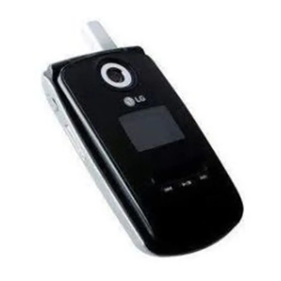
Related Manuals for LG L240


Summary of Contents for LG L240
- Page 1 Service Manual LG240_ME240 Date: September, 2006 / Issue 1.0...
-
Page 2: Table Of Contents
Table of Contents 1. Introduction ........5 4.18 Ear-Mic Headset MIC Trouble Shooting........88 1.1 Purpose........... 5 4.19 Ear-Mic Headset HSOR/HSOL 1.2 Regulatory Information......5 Trouble Shooting........89 2. Performance ........7 5. Downloading Software ....91 2.1 HW Feature..........7 5.1 The purpose of downloading software .. 91 2.2 Technical Specification ...... -
Page 4: Introduction
1. Introduction 1. Introduction 1.1. Purpose This manual provides the information necessary to repair, calibration, description and download the features of this model. 1.2. Regulatory Information A. Security Toll fraud, the unauthorized use of telecommunications system by an unauthorized part (for example, persons other than your company’s employees, agents, subcontractors, or person working on your company’s behalf) can result in substantial additional charges for your telecommunications services. - Page 5 1. Introduction E. Notice of Radiated Emissions This model complies with rules regarding radiation and radio frequency emission as defined by local regulatory agencies. In accordance with these agencies, you may be required to provide information such as the following to the end user. F.
-
Page 6: Performance
2. PERFORMANCE 2. Performance 2.1 HW Feature Item Feature Comment Form Factor Clamshell with External Display 1) Capacity Battery Standard : Li-Ion, 900mAh (LGC) 2) Packing Type : Soft Pack Standard : Size 89.0 X 47.0 X 22 mm Weight With Battery Volume 75cc... - Page 7 2. PERFORMANCE Item Feature Comment Status Indicator Indicator LED in MOD KEY Alphanumeric Key : 12 Function Key: Function Key : 12 4 Key Navigation, OK, Mod Key : 3 F1, F2, Camera, CLR, Keypad Side Key : 3 SND, END/PWR, MP3 Total No of Keys :30 Player Mod Key :...
-
Page 8: Technical Specification
2. PERFORMANCE 2.2 Technical Specification Item Description Specification GSM850 TX: 824 + n ¢• 0.2 MHz (n=1 ~ 124) RX: TX + 45 MHz GSM900 TX: 890 + n ¢• 0.2 MHz (n=1 ~ 124) 890 + (n-1024) ¢• 0.2 MHz (n=975 ~ 1023) RX: TX + 45 MHz Frequency Band DCS1800... - Page 9 2. PERFORMANCE Item Description Specification GSM850/GSM900 Offset from Carrier (kHz). Max. dBc 600~ <1,200 1,200~ <1,800 1,800~ <3,000 3,000~ <6,000 Output RF Spectrum 6,000 (due to modulation) DCS1800/PCS1900 Offset from Carrier (kHz). Max. dBc 600~ <1,200 1,200~ <1,800 1,800~ <3,000 3,000~ <6,000 6,000 GSM850/GSM900...
- Page 10 2. PERFORMANCE Item Description Specification DCS1800/PCS1900 Offset from Carrier (kHz). Max. (dBm) Output RF Spectrum (due to switching transient) 1,200 1,800 Spurious Emissions Conduction, Emission Status Bit Error Ratio BER (Class II) < 2.439% @-102dBm Rx Level Report accuracy 3 dB 8 3 dB Frequency (Hz) Max.(dB)
- Page 11 2. PERFORMANCE Item Description Specification STMR 13 5 dB Stability Margin > 6 dB dB to ARL (dB) Level Ratio (dB) 17.5 22.5 30.7 Distortion 33.3 33.7 31.7 25.5 Side Tone Distortion Three stage distortion < 10% <Change> System frequency 2.5ppm (13 MHz) tolerance <Change>32.768KHz tolerance...
- Page 12 2. PERFORMANCE Item Description Specification Antenna Bar Number Power 3.62V 0.03V Battery Indicator 3.70V 0.03V 3.78V 0.03V 3.91V 0.03V 3.92V 0.03V↑ 3.62V↓ 0.03V (Call) Low Voltage Warning 3.50V↓ 0.03V (Standby) Forced shut down Voltage 3.35 0.03 V 1 Li-ion Battery Standard Voltage = 3.7 V Battery Type Battery full charge voltage = 4.2 V...
-
Page 13: Circuit Description
3. Circuit Description 3. Circuit Description 3.1 General Description The RF part consists of a transmitter, a receiver, a synthesizer, a voltage supply and a VC-TCXO part. The main RF Chipset MMM6000 is a transceiver for the GSM, GPRS, and EDGE standards, providing antenna-todigital- bits functionality. - Page 14 3. Circuit Description 3.2.1.1 Front End Part The RF front end consists of Antenna Switch, quad saw filters and LNAs integrated in transceiver . Antenna switch is integrated in MMM6027 (Raptor) and quad saw filters are integrated in saw filter bank.
- Page 15 3. Circuit Description 3.2.2 Synthesizer Part Both the RX and TX VCO run at 3296 to 3820 MHz and have integrated resonators with 32 states of digital course tuning. The frequency synthesizer is a 24-bit, 3rd order fractional N synthesizer with digital AFC and a lock time of less than 80µs.
- Page 16 3. Circuit Description MM M600 0 Quad -B and Di gRF GSM/ GPRS/ EDGE TRANSCEI VER ˜4 ° Di gital R adio Fil t er ˜2 Receiver Modu l e ° Power Am plific at ion Ant e nn a Power Dete ction &...
- Page 17 3. Circuit Description 3.2.4 Digital Core The digital core of the MMM6000 consists of four major functional blocks: • Receive coprocessor (RxCPROC) • DigRF • Transmit module (TXM) • Transmit/receiver timing sequencer (TRXQ) 3.2.4.1 Receive coprocessor (RxCPROC) The digital portion of the RX signal processing chain, consisting of decimation filters, a digital LO generator, complex mixers, adjustable channel filters, and a DC adapt module.
- Page 18 3. Circuit Description 3.2.4.2 DigRF Interface to the baseband IC using the DigRF standard. The DigRF standard specifies the logical, electrical, and timing details of the RF/Baseband interface. Figure 5 shows the DigRF standard RF- baseband interface. RxTxDat a RxTxEn Ct r l Dat a Ct r l En Baseband...
-
Page 19: Digital Baseband
3. Circuit Description 3.3 Digital Baseband SDRAM Flash and SRAM OMAPV1030 EDGE multimedia platform Boot ROM Secure eFuse USB controller Host Secure RAM Test: Device E2TLM, BCM, SCM,DielD Security layer JTAG, FuseFarm OCP-I OCP-T2 OCP-T1 EMIFF EMIFS Traffic controller DSP MMU subsystem subsystem System... - Page 20 3. Circuit Description 3.3.2 Block Description The OMAPV1030 E-GPRS multimedia device is based on an OMAP3.4 platform that integrates: - The MPU subsystem - The DSP subsystem - A system DMA - A traffic controller providing: - External memory interfaces with: - A slow interface (EMIFS) to ROM, SRAM, FLASH memories - A fast interface (EMIFF) to SDRAM memories - Layer 3 (L3) interconnect made of two OCP target ports (OCP-T1 and OCP-T2) and one OCP...
- Page 21 3. Circuit Description The OMAP3.4 platform is the computing core of the device. The other OMAPV1030 components are organized as follows: - The internal memory subsystem is made of a single-port 256K-bit shared internal SRAM. - The security subsystem is a set of several components, including dedicated a secure mode to run secure applications.
- Page 22 3. Circuit Description OMAPV1030 device OMAPV1030 Radio I/F ULPDR GSM_clock_13M TPU BUS digitalrf_rf_clk TSPCLK RF CTRL IF digitalrf_rf_cs TSPEN TSPDO digitalrf_rf_data TSPDI RF real- digitalrf_tx_start TSPACT3 time IF digitalrf_enr TSPACT4 GSM_clock_26M CORE digitalrf_rxen TSPACT5 digitalrf_rx_clk CLKR MPU public TIPB digitalrf_rx_data digitalrf_rx_cs shared McBSP...
- Page 23 3. Circuit Description 3.3.5 UART Interface LG240 has Three UART Drivers as follow : - UART1 : USB - UART2 : ETM, Calibration - UART3 : AT command, Fax_modem, Bluetooth UART1(USB) Resource Name Description USB_DP Data USB_DM Data USB_PWR POWER USB_POWER VBUS VBUS...
- Page 24 3. Circuit Description Resource Inactive Active I/O # Net Name State State State I/O (1) DPD1 GPIO I/O (2) Sysboot HIGH I/O (3) DP_IO_ON GPIO HIGH I/O (4) USB_BOOT_SEL Sysboot LOW (Giant Plus) HIGH (Nanya) I/O(5) FOLDER_2 GPIO HIGH I/O (6) DPD0 GPIO I/O (7)
-
Page 25: Analog Baseband
3. Circuit Description 3.4 Analog Baseband 3.4.1 General Description The TRITON chip is the analog and power management part of the Texas Instruments next generation wireless terminal. These GSM/GPRS/E-GPRS, 3G W-CDMA, CDMA2000 platforms are composed of a digital baseband processor, a RF chip, an application processor OMAP and of different peripheral devices like a LCD panel, a Multi-Media Card, a Bluetooth modem, a GPS modem. - Page 26 3. Circuit Description 3.4.2 Audio Signal Processing & Interface The Audio module consists of a Voice Codec dedicated to mobile telephone terminal application and a Stereo path. - The Voice Codec circuit processes analog audio components in the uplink path and transmits the converted data to the DSP speech coder through the voice serial port (VSP).
- Page 27 3. Circuit Description <Fig.10> Power Supply Scheme - 28 -...
- Page 28 3. Circuit Description 3.4.4 Monitoring ADC The monitoring ADC (MADC) consists of a 10-bit analog-to-digital converter (ADC) combined with an 11- input analog multiplexer. The ADC implementation consists of a successive approximation conversion. Five of the eleven inputs are available externally (ADIN1..5), and the remaining six inputs are dedicated to die temperature measurement, main battery voltage, backup battery voltage, charger voltage, charger current monitoring and USB Vbus voltage.
- Page 29 3. Circuit Description 3.4.6 Memories - 512Mbit NOR Flash + 256Mbit DDR SDRAM - Address and Data Muxed type (Data : FDATA0 ~ FDATA15, address : FDATA0 ~ FDATA15 and FADD17 ~ FADD24 ) 3.4.7 LCD module pin description LCD module is connected to main board with 40 pin FPCB. The LCD module includes receiver & vibrator - 30 -...
- Page 30 3. Circuit Description Pi n # NAME De scri pti on Dat a Write Enable M_CS Main LCD Select _LCD_RESET Main/Sub LCD Reset _S_CS Sub LCD Select D(0) LCD Dat a D(1) LCD Dat a D(2) LCD Dat a D(3) LCD Dat a D(4) LCD Dat a...
- Page 31 3. Circuit Description 3.4.8 Keypad Map description KEYPAD VREXTH VRIO R535 U503 LMV7291MGX-NOPB 100K U501 FSA4157L6X VIN- PWON VIN+ R516 R536 KBR(5) C501 C502 200K 0.1u 4.7u VA501 STAR KB_501 KB_502 KB_503 SEND R520 KBR(0) EVL5M02200 KB_504 KB_505 KB_506 KB501 CLEAR VA502 R522...
- Page 32 3. Circuit Description 3.4.9 Bottom System Connector Pin # LG240 Description 24Pin VRIO(1.8V) TEST : JTAG Reference Voltage(1.8V) HANDFREE Hand free POWER(VCHG) CHARGING (VCHG) POWER(VCHG) CHARGING (VCHG) POWER ON(RPWON) TEST (RPWON) TEST :JTAG TEST : JTAG TEST : JTAG USB_DM / RX USB/UART2 (Receive Data) TEST : JTAG POWER GND...
-
Page 33: Bluetooth Interface
3. Circuit Description 3.5 Bluetooth Interface 3.5.1 Bluetooth Circuit VRIO VBAT R307 KA_OUT R310 VLDO_OUT R308 C306 C307 VLDO_OUT C308 0.1u 0.1u 4.7u C310 CLK_32K ANA_OUT R313 BT_CLK_REQ IO0_EXT_CLK_REQ_OUT RF_P IO1_EXT_CLK_REQ_IN RF_M IO2_SCL JTAG_TDI ANA_OUT KA_OUT RFIO_OUT IO3_SDA JTAG_TDO JTAG_TMS JTAG_TCK HCI_TX BT_RX... - Page 34 3. Circuit Description 3.5.2 Pin Description Description CLOCKS/GLOBAL SIGNALS SLOW-CLK_IN 32.768.kHz clock input XTALM Negative fast crystal in XTALP/FAST_CLK_IN Positive fast crystal in/fast clock input RADIO FREQUENCY INTERFACE Receiver/transmit differential RF I/O Receiver/transmit differential RF/IO POWER MANAGEMENT VLDC_OUT Very-low drop-output voltage KA_OUT Keep alive output NSHUT_DOWN...
- Page 35 3. Circuit Description 3.5.3 Bluetooth circuit Description One chip Bluetooth Module U302(BRF6150) supports the following feature. -Bluetooth®1.2 Support A2DP, HFP,HSP Adaptive Frequency Hopping (AFH) Fast connection Extended SCO-All New Paket Types Scatter Mode Quality-Of-Service Improvements LMP Improvements Synchronization -UART Interface Baud Rate: 115.2kbps (default) -USB Interface v.2.0 -PCM Interface...
-
Page 36: Trouble Shooting
4. TROUBLE SHOOTING 4. TROUBLE SHOOTING 4.1 RF Part Technical Brief 4.1.1 RF Part Component SW701 U701 FL701 U704 X701 U703 U702 ] Part Description SW701 : Mobile Switch Connector U701 : Power Amp Front End Module (MMM6027) U702 : RF Transceiver (MMM6000) U703 : 1.8V Regulator U704 : 2.8V Regulator FL701 : SAW Filter Bank... - Page 37 4. TROUBLE SHOOTING 4.1.2 Part Description 4.1.2.1 Regulator Supply 2.8V to Analog RF part, 1.8V to Digital RF part. VBAT VCC_1.8V C747 TPS79918DRVR U703 C744 R714 VRIO 2.2u PGND C745 C746 0.1u 0.01u U704 VBAT VCC_2.8V TPS79928DRVR U704 C747 R715 SYSCLKEN 2.2u 100K...
- Page 38 4. TROUBLE SHOOTING 4.1.2.2 VCTCXO Produce RF and BB reference Clock - 26MHz Clock. C741 X701 VCC_2.8V C741 330p XTAL XTAL VCC_1.8V X701 R711 VCONT R718 100K C743 C742 100K 26MHz C742 <Fig.2> VCTCXO Circuit Diagram 4.1.2.3 Power Amplifier Front End Module (MMM6027) Select the RX / TX path and amplifier the power.
- Page 39 4. TROUBLE SHOOTING VBAT VCC_2.8V C702 C703 C704 VDETECT C707 C708 C709 C710 C711 RX_PCS_OUT C713 0.01u CAP_LB1 RX_DCS_OUT C714 1000p CAP_LB2 RX_EGSM_OUT C716 4700p CAP_HB1 RX_GSM850_OUT C717 1000p U701 CAP_HB2 MMM6027 TX_LB_IN TX_HB_IN TX_EN TX_ANT_SW_EN C721 LB_HB C720 US_EURO IPC_BCM C722 R703...
- Page 40 4. TROUBLE SHOOTING 4.1.2.4 SAW Filter Bank Pass wanted signal and include LNA matching circuit. C712 C719 FL70 1 FL701 C712 GSM850_RX_IN PCS_RX2_OUT EGSM_RX_IN PCS_RX1_OUT C715 DCS_RX_IN DCS_RX2_OUT PCS_RX_IN DCS_RX1_OUT EGSM_RX2_OUT GND4 EGSM_RX1_OUT C718 GND3 GSM850_RX2_OUT GND2 GSM850_RX1_OUT GND1 C719 SAQHJ881MAB0F00 <Fig.4>...
- Page 41 4. TROUBLE SHOOTING 4.1.2.5 RF Transceiver (MMM6000) Digital Interface to Baseband. Integrate LNA and VCO circuit. C739 C740 U702 C738 VCC_2.8V R703 R706 C723 VCC_1.8V VCC_2.8V VCC_2.8V R704 R705 R707 R708 VCC_2.8V C726 C727 C728 1.8p C730 C731 C732 2.2u C735 C736 SYSCLK...
-
Page 42: Rf Part Trouble Shooting
4. TROUBLE SHOOTING 4.2 RF Part Trouble shooting 4.2.1 RF Receiving Path Trouble Shooting START SW701 HP8960 : Test mode 190 CH, 5 level setting (TCH) 190 CH, -60dBm setting (BCCH) Spectrum analyzer setting Oscilloscope setting U701 SW701 1. Check Regulator Circuit FL701 U704... - Page 43 4. TROUBLE SHOOTING 4.2.1.1 Regulator Circuit C74 7 Regulator U70 4 C747(C744) 2.8V(1.8V)? Regulator is OK. R71 5 R71 4 Replace U704 R715(R715) High? (U703) U70 3 Check U101 C74 4 VBAT VCC_1.8V TPS79918DRVR U703 C747 C744 R714 VRIO 2.2u PGND C745 C746...
- Page 44 4. TROUBLE SHOOTING 4.2.1.2 VCTCXO Circuit C741 W_PCSX AW_PCS X701 VCC_2.8V C741 330p EXTAL XTAL VCC_1.8V X701 C743 R711 VCONT R718 100K C743 C742 R711 100K 26MHz C742 VCTCXO C741 C741 26MHz? VCTCXO is OK. C743 0.9V? Check R711&R718 C742 2.8V? Replace X701 C743 Check U102...
- Page 45 4. TROUBLE SHOOTING 4.2.1.3 Mobile Switch & PAFEM & SAW Bank Circuit Mobile Switch SW701 C75 0 Replace SW701 SW701 between C701 and C750 Is short? C70 1 PAFEM * Refer to the table.1 C72 4 Check Control Signal Check U702 C722,C724,C725,C733,C734 C72 5 U70 1...
- Page 46 4. TROUBLE SHOOTING 4.2.1.4 RF Main Transceiver Circuit VCC_2.8V R706 C723 VCC_1.8V VCC_2.8V VCC_2.8V R708 VCC_2.8V C726 C727 C728 1.8p C730 C731 C732 2.2u C735 C736 C739 2.2u C740 SYSCLK SYSCLKEN SYSCLKEN C737 BT_CLK BT_CLK_EN BT_CLK_REQ AUX_CLK PAC_DET VDETECT U702 C738 DIGITALRF_ENABLE 4700p...
- Page 47 4. TROUBLE SHOOTING 4.2.2 RF Transmitting Path Trouble Shooting START SW701 HP8960 : Test mode 190 CH, 5 level setting (TCH) 190 CH, -60dBm setting (BCCH) Spectrum analyzer setting Oscilloscope setting U701 SW701 1. Check Regulator Circuit U704 2. Check X701 VCTCXO Circuit U703...
- Page 48 4. TROUBLE SHOOTING 4.2.2.1 Mobile Switch & PAFEM Circuit Mobile Switch SW701 Replace SW701 SW701 between C701 and C750 C75 0 Is short? C70 1 PAFEM * Refer to the table.1 C72 4 Check Control Signal Check U702 C722,C724,C725,C733,C734 R70 4 C72 5 U70 1 R70 5...
- Page 49 4. TROUBLE SHOOTING LB_HB TX_ANT_SW_EN <GSM850> <PCS1900> C711 - 50 -...
-
Page 50: Bluetooth Trouble Shooting
4. TROUBLE SHOOTING 4.3 Bluetooth Trouble Shooting start In Engineering mode(2945#*#) Set BT Test mode ON Set RF test mode and thenBT ON Check BT Antenna Status Replace BT Antenna (Refer to figure 1) Check 1.8V from ABB Check ABB(U101) (Refer to figure 2) Check 26MHz Check VCTCXO or... - Page 51 4. TROUBLE SHOOTING 4.3.1 Checking BT Antenna 4.3.1.1 Visual Inspection <Fig. 1> Fix to Silk screen Fix to Edge 4.3.1.2 Checking BT VRIO Checking pin A3,D8,H6(R307) 1.8V High Check ABB Check 1.8V High C306 R307 Check BT_CLK <Fig. 2> - 52 -...
- Page 52 4. TROUBLE SHOOTING 4.3.1.3 Checking BT_CLK BT CLK Checking VCTCXO 26MHz C741 R317 Check BT CLK(E2) Check BT_CLK_REQ <Fig. 3> 4.3.1.4 Checking BT CLK REQ Checking BT_CLK_REQ Check BT_CLK_REQ BT CLK REQ C313 1.28s SYS_CLK_EN BT_CLK_REQ <Fig. 3> <Sleep Mode> - 53 -...
- Page 53 4. TROUBLE SHOOTING 4.3.1.5 Checking BT RF OUT RFIO_OUT DBF81H903 FB301 RF_P GND1 R326 ANT301 UNBL R327 R328 C334 RF_M ANT302 100p Check with Spectrum Analyzer in BT Equipment connection status. - 54 -...
-
Page 54: Baseband Part Troubleshooting
4. TROUBLE SHOOTING 4.4 Baseband Part Troubleshooting 4.4.1 Power On Trouble 4.4.1.1 Power-On Trouble Troubleshooting Power-On Sequence - Connecting Battery - Power-On Key Detection - Pwon signal goes to ABB and then ABB resets DBB by ONNOFF signal - ONNOFF turns low(0v) to High (2.8V) and it resets DBB (Neptune) - All LDOs (internal LDOs of ABB and external LDOs) are turned on Check Points - Battery Voltage... - Page 55 4. TROUBLE SHOOTING 4.4.2 Check Point C130 C127 C128 U101 C133 (Tripton) C134 C129 C125 C126 C131 C130 <Fig. 2> Triton Power Supplies C125 : VREXTL : 1.8v - for Camera, LCD Pwon C126 : VREXTH : 2.8v - for Camera, Folder S/W, Level shifter, Pull up of Temp C127 : VRMMC : 2.85v - T-flash C128 : VRSIM : 1.8 / 2.85v - SIM C129 : VRUSB : 3.3v (when USB cable connected)
- Page 56 4. TROUBLE SHOOTING <Fig. 2.1> Triton Power Supplies - 57 -...
- Page 57 4. TROUBLE SHOOTING 4.4.3 Charging Trouble Shooting - Charging method : CC-CV - Charger Detection Voltage : About 5.2V - Charging Time : About 3H under - Charging Current : About 550mA - Cut-off Current : 120mA - Low Battery Alarm z Talk mode : 3.62V z Standby mode : 3.50V - Switch-Off Voltage : 3.35...
- Page 58 4. TROUBLE SHOOTING 4.4.4 Charging Current - Charging Procedure z Connecting TA & Charger Detection z Control the charging Current by ABB z Charging Current flow into the Battery - Check Points z Connection of TA z Charging Current Path z Battery - Trouble Shooting Setup z Connect Battery &...
- Page 59 4. TROUBLE SHOOTING START I/O Connector (CN401) Re-solder the CN401 Is well-soldered? (Pin 12,13) Voltage at pin 4,6 of Q101 The TA is out of order. =5.2v ? Change the TA Q101,D101,R103 Re-solder Is well-soldered ? Q101,D101,R103 Voltage across R103 Replace Q101, D101 Is about ~130mV ? The Battery may have Problem...
-
Page 60: Lcd Display Trouble
4. TROUBLE SHOOTING 4.5 LCD Display Trouble z LCD Control signals from Main Board - LCD_RST, LCD_CS, LCD_ADS, MLED, LCD_D(0)~LCD_D(15) z Check Point - The Assembly status of the LCD Module - The Soldering of connector - The FPCB which connects the LCD Module z Trouble Shooting Setup - Connect PIF Jig, and Power on EMI Filter (Total 9ea) - Page 61 4. TROUBLE SHOOTING z Check Point - The Assembly status of the LCD Module - The Soldering of connector - The FPCB which connects the LCD Module LCD Module Connector Check Point - LCD Glass : Crack or Break? FPCB Connector (LCD Module Side) Check Point - FPCB : Crack or Break? FPCB Connector (Mainboard Side)
- Page 62 4. TROUBLE SHOOTING Pin NO.20 Pin NO.1 Pin NO.40 Pin NO.21 < LCD Connector of a Main FPCB> L_A(1) L_WR <Normal Signal during display> - You must check signals LCD Connector Side of a Main FPCB because you could check final signal states through EMI Filter, connector, FPCB and etc.
- Page 63 4. TROUBLE SHOOTING START Refer to Power is supplied to Power On Trouble the board? First of all, push a key pad then check 1.8/2.8V check Points during a Key pad LED ON. Connection between Reconnect FPCB FPCB and boards is OK? CN601 is soldered well? Re-solder the CN601 Re-solder...
-
Page 64: Camera Trouble Shooting
4. TROUBLE SHOOTING 4.6 Camera Trouble Shooting z Check Points - Check the power supply - Check the soldering of Components - Check the CAMERA signals z Trouble Shooting Setup - Enter the engineering mode. - Go to menu ‘Baseband → Camera → Main LCD Preview ’ VGA Camera 2.8V Point 1.8V Point... - Page 65 4. TROUBLE SHOOTING START Refer to Power is supplied to Power On Trouble the board? → → First of all, Go to menu ëB aseband Camera Main LCD Preview Refer to LCD Display OK? LCD Display Trouble Connection between Reconnect FPCB FPCB and boards is OK? Re-solder Paths of Camera control...
-
Page 66: Mod Key Trouble Shooting
4. TROUBLE SHOOTING 4.7 MOD Key Trouble Shooting z Check Points - Check the MOD Key FPCB - Check the soldering of Components - Check the MOD signals z Trouble Shooting Setup - Connect PIF Jig, and Power on MOD Key Signal Pin MOD LED Signal Pin <... - Page 67 4. TROUBLE SHOOTING VBAT VCHG R406 100ohm VBAT R408 U402 DG2011DX-T1-E3 FSA4157L6X U401 MOD_LED REGEN C403 C402 C406 MODIND_LED R412 0.1u 0.1u VA401 < MOD LED Circuit > START The MOD LED OK? The MOD Key input OK? The MOD Key is OK. Change the board.
- Page 68 4. TROUBLE SHOOTING If you push a MOD Key, Change U402 Could yor watch a voltage above 3V If not OK, Change U401 at the MOD FPCB LED Pin? MOD FPCB OK? Replace or Rework the MOD FPCB Crack or soldered well? Connection between Reconnect FPCB Main FPCB and LCD Module/Main Board...
- Page 69 4. TROUBLE SHOOTING Replace or Rework the MOD FPCB Check resistor(R128) on mainboard. MOD Signal Pin Voltage OK? Check voltage at the R128. It Must be 1.8V. Initial state is 1.8V. If you push a button, pin voltage must drop below 1.5V. Connection between Reconnect FPCB Main FPCB and LCD Module/Main Board...
-
Page 70: Sim Detect Trouble Shooting
4. TROUBLE SHOOTING 4.8 SIM Detect Trouble Shooting SIM interface scheme is shown below. SIM_IO, SIM_CLK, SIM_RST ports are used to communicate DBB with ABB and the Charge Pump in ABB enables 1.8V/3V SIM operation. SIM CONNECTOR C209 VRSIM R211 R211 SIM_PWRCTRL SIM_RST... - Page 71 4. TROUBLE SHOOTING START Insert SIM The soldering of SIM Resolder the J201.. connector is OK? Resolder the The all paths connected R211, R218, C206, C207, C208, C209 to J201 are OK? POWER ON Check the SIM_RST, SIM_CLK, SIM_IO, VRSIM The SIM Card is OK? SIM card is broken.
-
Page 72: Folder On/Off And Trouble Shooting
4. TROUBLE SHOOTING 4.9 Folder On/Off and Trouble Shooting Folder Operation scheme is shown below. FOLDER SWITCH VRIO VREXTH VREXTH U408 SN74LVC2T45YZPR U502 A3212EELLT-T VCCA VCCB UART2_RX DEBUG_RX R444 FOLDER_2 FOLDER FOLDER C408 C503 C504 0.1u 0.1u 0.1u 4.9.1 Folder Operation(ON/OFF) - There is a magnet to detect the folder status, opened or closed. - Page 73 4. TROUBLE SHOOTING 4.9.2 Folder Trouble (ON/OFF) START The all paths connected Resolder the to U502 are OK? R537,C503,C504,R44 Is the VREXTH a 2.8V? Refer to Power ON Is the VRIO a 1.8V? Trouble Folder signal is low on Replace the U502. Magnetizing into U502? The U502 is broken Folder_2 signal is low on...
-
Page 74: Speaker Trouble Shooting
4. TROUBLE SHOOTING 4.10 Speaker Trouble Shooting START Disassemble the rear case of phone. Speaker has a Check the resistance between problem. SPK_P & SPK_N of the Speaker Replace the Speaker. With the DVM ~ 8 ohm Disconnect The F-PCB from the Main Board. - Page 75 4. TROUBLE SHOOTING U102(DBB) is broken. Check the SPK_EN( R333) Change the board. Is SPK_EN a High? Play the Ring tone. Check the input(R330,R332) of U303 The signal is a Analog U303 is broken. Replace the U303. <Fig.2> INPUT(R330) of U303 <Fig.3>...
- Page 76 4. TROUBLE SHOOTING Check the soldering of Resolder the R329, R329, R331, C335, C336,R330, R332 R331,C335,C336,R330,R332 Soldering is OK? Play the Ring tone. U102(DBB) is broken. Check the R329(SPKNA),R331(SPKPA) Change the board. The signal is a Analog Check the Speaker contact PAD of the F-PCB - 77 -...
-
Page 77: Receiver Trouble Shooting
4. TROUBLE SHOOTING 4.11 Receiver Trouble Shooting C620 C621 START L601L602 Disassemble the upper case of phone. Receiver has a Check the resistance between SPK_P & SPK_N of the Receiver problem. With the DVM ~ 32 ohm Replace the Receiver. Disconnect the F-PCB from the Main Board. -
Page 78: Mic Trouble Shooting
4. TROUBLE SHOOTING 4.12 MIC Trouble Shooting z MIC Operation scheme is shown below. R132 C111 0.1u MICIN MICIN R133 C112 0.1u MICIP MICIP HSMIC HSMICIP C215 C215 MICBIAS MICBIAS HSMICBIAS HSMICBIAS C215 C215 AUXI_FMR AUXI EARN RCV_N R318 MICBIAS Close to MIC C327 C328... - Page 79 4. TROUBLE SHOOTING z MIC Trouble START MICBIAS Voltage of U101 Voltage across Rxxx Replace U101 is about 2.5V? is about 2.5V? Re-solder Rxxx & Rxxx Check the signal Replace level at each side of MIC301. MIC301 Is it a few tens mVAC? Check the soldering of Replace U101 Rxxx,Rxxx,Cxxx,Cxxx...
-
Page 80: Transflash Trouble Shooting
4. TROUBLE SHOOTING 4.13 Transflash Trouble Shooting z Transflsh Operation scheme is shown below. R204 AA14 R203 TF_CLK MMC1_CLK R205 TF_DAT0 MMC1_DAT0 R201 R202 AA13 TF_DAT1 MMC1_DAT1 TF_DAT2 MMC1_DAT2 TF_DAT3 MMC1_DAT3 TF_CMD MMC1_CMD R140 FOLDER GPIO_33 MMC1_PBIAS C136 VRMMC S201 S201 SCHB1A0202 TF_DAT2... - Page 81 4. TROUBLE SHOOTING z VRMMC Signal(Power ON) <VRMMC Signal when T-Flash is inserted> <VRMMC Signal when T-Flash is not inserted> z TF_DAT0 Signal (Music Play) <TF_DAT0 Signal while T-Flash is read> - 82 -...
-
Page 82: Keypad Backlight Led Trouble Shooting
4. TROUBLE SHOOTING 4.14 Keypad Backlight LED Trouble Shooting z Keypad backlight LED Operation scheme is shown below. VBAT R517 Q501 KEY_LED_EN 2SC5585 R518 R517 Q501 z Backlight operation - Keypad backlight LED is controlled with KEY_LED_EN signal - KEY_LED_EN signal from DBB(U102) - The LEDs are forward biased and turned on z Check Point - VBAT level ( 3.35 ~4.2V) - Page 83 4. TROUBLE SHOOTING z KEY Backlight LED Trouble START Is the Voltage level VBAT Charge Battery 3.35 ~4.2? Check the soldering of each Are all LEDs LD501 ~514 R or Replace LESs not Working? working Check the condition of Q501 is Q501 Working? If problem, Replace Q501...
-
Page 84: Vibrator Trouble Shooting
4. TROUBLE SHOOTING 4.15 Vibrator Trouble Shooting z Vibrator operation scheme is shown below LED_A LED_B LED_C VIBDR VIBRATOR CKEN SYSCLKEN 21 pin REGEN REGEN R117 HSDET HSDET R119 BM_SEL R121 BM_PRECH VBACKUP VIBRATOR MODIND_LED Soldering check z Vibrator Trouble START ABB(U101) has a problem. -
Page 85: Ear-Mic Jack Detection Trouble Shooting
4. TROUBLE SHOOTING 4.16 Ear-Mic Jack Detection Trouble Shooting START Disassemble the rear case of phone. Connect the Ear-Mic Headset to the Ear-Mic Socket of phone. Re-solder Check the Ear-Jack Detection. R305, Is the status of R314 low? R312,C302,C317,R314 Re-solder Pin #2 & #3 of Check the soldering status J301 Of J301. -
Page 86: Ear-Mic Hook Detection Trouble Shooting
4. TROUBLE SHOOTING 4.17 Ear-Mic Hook Detection Trouble Shooting START Disassemble the rear case of phone. Connect the Ear-Mic Headset to the Ear-Mic Socket of phone. Ear-Mic Headset has a Press the HOOK Button. problem. Is the status of C305 LOW? Exchange the Ear-Mic Headset Is the status of R306... -
Page 87: Ear-Mic Headset Mic Trouble Shooting
4. TROUBLE SHOOTING 4.18 Ear-Mic Headset MIC Trouble Shooting START Check the resistance between Ear-Mic Headset has a MIC & GND of the Headset. problem. Less than 2.2 kOhm? Exchange the Ear-Mic Headset Disassemble the rear case of phone. Connect the Ear-Mic Headset to the Ear-Mic Socket of phone. -
Page 88: Ear-Mic Headset Hsor/Hsol Trouble Shooting
4. TROUBLE SHOOTING 4.19 Ear-Mic Headset HSOR/HSOL Trouble Shooting START Ear-Mic Headset has a Check the resistance between problem. HSOR/L & GND of the Headset. ± Exchange the Ear-Mic 16 0hm 15%? Headset Disassemble the rear case of phone. Connect the Ear-Mic Headset to the Ear- Mic Socket. - Page 89 4. TROUBLE SHOOTING z Ear-Mic Headset Operation scheme is shown below. R301 EAR JACK HSMICBIAS VRIO C301 R302 VRIO 200K LMV7291MGX-NOPB VIN- R304 HOOKDET VIN+ U301 R305 C302 R306 J301 L301 C303 0.1u R309 HSMICIP 100nH C304 C305 VA301 VA302 VA303 Close to Ear-Jack C309...
-
Page 90: Downloading Software
5. Downloading Software 5. Downloading Software 5.1 The purpose of downloading software 5.1.1 To make a phone operate at the first manufacturing - A phone = Hardware + Software - A phone cannot operate with hardware alone. - The hardware with the suitable software can operate properly. 5.1.2 To upgrade the software of the phone - The software of the phone may be changed to enhance the performance of the phone. - Page 91 5. Downloading Software The Environment of Downloading Software. 5.2.2 In case of using the PIF( MON Port) LG240 Handset PC with RS-232 POWER SUPPLY a. Preparation - Target Handset (LG240) - PIF - RS-232 Cable and PIF-to-Phone interface Cable (T.I) - Power Supply or Battery b.
-
Page 92: Download Procedure
5. Downloading Software 5.3 Download Procedure A. Computer Program file -> MultiGSM.EXE Click 1. Copy "GSMULTI" Folder. Paste in " C:\" → 2. Execute "GSMULTI.reg file" Registered at PC 3. "MultiGSM.exe" execution file B. Click the “Setting” button. Then, choose Configuration which is going to download. →... - Page 93 5. Downloading Software C. Computer Program file -> MultiGSM.EXE Click 5. Configuration : select values like below C;\GSMULTI\MODEL\LG240\LG240.dll Phone software select( m32 file) C:\GSMULTI\MODEL\LG240\csst_gsample256Mbit_dnld_startup.out Download speed Start Comport END Comport Not use dll internal Frame count select D. Computer Program file -> MultiGSM.EXE Click 6.
- Page 94 5. Downloading Software E. After “Start Button”, Which Stand-by condition → → 7. Stand-by condition "TI(EX) : Wait ASIC" is displayed connect the Phone F. SW downloading condition Downloading : Start - 95 -...
- Page 95 5. Downloading Software G. SW downloading END condition - 96 -...
-
Page 96: Block Diagram
6. BLOCK DIAGRAM 6. BLOCK DIAGRAM LG240 Block Diagram(RF) Dig RF Interface - 97 -... - Page 97 6. BLOCK DIAGRAM LG240 Block Diagram(BB) VRSIM UART3_RX UART3_TX UART3_CT S UART3_RT - 98 -...
-
Page 98: Circuit Diagram
UART1 MODEL Designer JM KIM 2.5G 2006 UART_RXD UART_TXD UFLS Checked ON_SW ON_SW RPWON VRDBB VBAT VBAT DRAWING ABB/DBB URXD NAME UTXD Approved C151 UART_RTS UART_CTS DRAWING Rev 1.1 LG Electronics Inc. Iss. Notice No. Date Name - 99 -... - Page 99 0 ohm Section Date Sign & Name Sheet/ Sheets MODEL LG240 06/30 Designer JM KIM 2006 Checked DRAWING MEMORY / T-FLASH / SIM / LDO NAME Approved DRAWING Iss. Notice No. Date Name LG Electronics Inc. Rev 1.1 - 100 -...
- Page 100 Sheets MODEL SPK_EN _SHDN LG240 C339 C340 06/30 SPK_P Designer DH KIM 2006 GND1 C341 33nF 33nF GND2 SPK_N Checked C342 C343 DRAWING AUDIO/BLUETOOTH NAME Approved DRAWING Iss. Notice No. Date Name LG Electronics Inc. Rev 1.1 - 101 -...
- Page 101 Sheet/ Sheets MODEL LG240 06/30 R435 Designer JM KIM 2006 100K USB_BOOT_SEL BOOT_SEL Checked R437 R438 Q401 DRAWING USB_PWR IO CONNECTOR & INDICATOR 2SC5585 NAME Approved DRAWING Iss. Notice No. Date Name LG Electronics Inc. Rev 1.1 - 102 -...
- Page 102 EVL5M02200 EVL5M02200 Section Date Sign & Name Sheet/ Sheets MODEL LG240 06/30 Designer JM KIM 2006 Checked DRAWING KEY & LED & HALL SWITCH NAME Approved DRAWING Iss. Notice No. Date Name LG Electronics Inc. Rev 1.1 - 103 -...
- Page 103 Date Sign & Name Sheet/ DP_IO_ON Sheets MODEL LG240 06/30 Designer JM KOO 2006 Q601 3 Checked DRAWING CAMERA & LCD & CHARGE PUMP NAME Approved DRAWING Iss. Notice No. Date Name LG Electronics Inc. Rev 1.1 - 104 -...
- Page 104 LG240 06/30 Designer JS YOO 2006 VBAT VCC_2.8V Checked TPS79928DRVR U704 DRAWING RF_Freescale NAME C747 R715 Approved SYSCLKEN 2.2u 100K PGND C748 C749 0.1u 0.01u DRAWING Iss. Notice No. Date Name LG Electronics Inc. Rev 1.1 LGIC(42)-A-5505-10:01 - 105 -...
-
Page 105: Pcb Layout
8. PCB Layout - 106 -... - Page 106 8. PCB Layout - 107 -...
- Page 107 - 108 -...
-
Page 108: Rf Calibration
9. RF Calibration 9. RF Calibration 9.1 RF Calibration Equipment Setup GSM Test Set(8960) GPIB control Power Supply Battery Simulator 9.2 RF Calibration Procedure a. Connect as above Fig. b. Set the power supply voltage about 4.2V c. Execute HK_23.exe - 109 -... - Page 109 9. RF Calibration Then, you can see the HotKimchi Revolution d. Set the 3 setting parameter on setting menu - 110 -...
- Page 110 9. RF Calibration e. Click the Apply button after selecting a model name f. Click the Calibration Start button - 111 -...
- Page 111 - 112 -...
-
Page 112: Exploded View & Replacement Part List
10. EXPLODED VIEW & REPLACEMENT PART LIST 10.1 EXPLODED VIEW 45 49 59 72 63 74 53 54 50 43 70 60 61 57 66 47 51 52 15 6 3 14 - 113 -... - Page 113 - 114 -...
-
Page 114: Replacement Parts
10. EXPLODED VIEW & REPLACEMENT PART LIST 10.2 Replacement Parts Note: This Chapter is used for reference, Part order <Mechanic component> is ordered by SBOM standard on GCSC Location Level Description Part Number Specification Color Remark GSM(FOLDER) TGFF0086501 Black AAAY00 ADDITION AAAY0153801 Black... - Page 115 10. EXPLODED VIEW & REPLACEMENT PART LIST Location Level Description Part Number Specification Color Remark MCJK00 COVER,FRONT MCJK0054401 MOLD, PC LUPOY SC-1004A, , , , , Dark Gray MDAG00 DECO,FRONT MDAG0017601 MOLD, PC LUPOY SC-1004A, , , , , Silver MPBH00 PAD,MIKE MPBH0018901...
- Page 116 10. EXPLODED VIEW & REPLACEMENT PART LIST Location Level Description Part Number Specification Color Remark MBJA00 BUTTON,DIAL MBJA0020503 COMPLEX, (empty), , , , , Black MCCE00 CAP,RECEPTACLE MCCE0030302 MG210c CAP RECEPTACLE Black MCCF00 CAP,MOBILE SWITCH MCCF0032901 MOLD, PC LUPOY SC-1004A, , , , , Silver MCCH00 CAP,SCREW...
-
Page 117: Main Component
10. EXPLODED VIEW & REPLACEMENT PART LIST <Main component> Note: This Chapter is used for reference, Part order is ordered by SBOM standard on GCSC Location Level Description Part Number Specification Color Remark SACY00 PCB ASSY,FLEXIBLE SACY0045901 SACE00 PCB ASSY,FLEXIBLE,SMT SACE0041101 PCB ASSY,FLEXIBLE,SMT SACC00... - Page 118 10. EXPLODED VIEW & REPLACEMENT PART LIST Location Level Description Part Number Specification Color Remark 3 V,1.2 mAh,COIN ,MATUESHITA Backup BATTERY SBCL00 BATTERY,CELL,LITHIUM SBCL0001001 (ML414/F9D) SJMY00 VIBRATOR,MOTOR SJMY0006503 3 V,0.08 A,10*3.45 ,17mm double tape MAIN ,128*160 ,33.8*46.24 ,262k ,TFT ,TM ,M_LGDP4511 SMLM00 LCD MODULE SVLM0018602...
- Page 119 10. EXPLODED VIEW & REPLACEMENT PART LIST Location Level Description Part Number Specification Color Remark C119 CAP,CERAMIC,CHIP ECCH0009512 1000 pF,25V ,K ,X7R ,HD ,0603 ,R/TP C120 CAP,CERAMIC,CHIP ECCH0010201 10 uF,6.3V ,M ,X5R ,TC ,1608 ,R/TP C122 CAP,CERAMIC,CHIP ECCH0010201 10 uF,6.3V ,M ,X5R ,TC ,1608 ,R/TP C123 CAP,CERAMIC,CHIP ECCH0007901...
- Page 120 10. EXPLODED VIEW & REPLACEMENT PART LIST Location Level Description Part Number Specification Color Remark C206 CAP,CERAMIC,CHIP ECCH0009515 150 pF,25V ,K ,X7R ,HD ,0603 ,R/TP C207 CAP,CERAMIC,CHIP ECCH0009515 150 pF,25V ,K ,X7R ,HD ,0603 ,R/TP C208 CAP,CERAMIC,CHIP ECCH0000182 0.1 uF,10V ,K ,X5R ,HD ,1005 ,R/TP C209 CAP,CERAMIC,CHIP ECCH0000115...
- Page 121 10. EXPLODED VIEW & REPLACEMENT PART LIST Location Level Description Part Number Specification Color Remark C403 CAP,CERAMIC,CHIP ECCH0009101 0.1 uF,6.3V ,K ,X5R ,TC ,0603 ,R/TP C404 CAP,CERAMIC,CHIP ECCH0004904 1 uF,6.3V ,K ,X5R ,TC ,1005 ,R/TP C405 CAP,CERAMIC,CHIP ECCH0000182 0.1 uF,10V ,K ,X5R ,HD ,1005 ,R/TP C406 CAP,CERAMIC,CHIP ECCH0004904...
- Page 122 10. EXPLODED VIEW & REPLACEMENT PART LIST Location Level Description Part Number Specification Color Remark C714 CAP,CERAMIC,CHIP ECCH0000143 1 nF,50V,K,X7R,HD,1005,R/TP C715 CAP,CHIP,MAKER ECZH0000830 33 pF,50V ,J ,NP0 ,TC ,1005 ,R/TP C716 CAP,CHIP,MAKER ECZH0001106 4700 pF,25V ,K ,X7R ,HD ,1005 ,R/TP C717 CAP,CERAMIC,CHIP ECCH0000143...
- Page 123 10. EXPLODED VIEW & REPLACEMENT PART LIST Location Level Description Part Number Specification Color Remark CN401 CONNECTOR,I/O ENRY0000801 24 PIN,0.5 mm,ETC ,Au ,BAT ZERO CONNECTOR, 60 PIN,0.4 mm,STRAIGHT ,AU ,STACKING HEIGHT 1.5 / CN601 ENBY0013008 BOARD TO BOARD SOCKET FOR LCM FPCB D101 DIODE,SWITCHING EDSY0012101...
- Page 124 10. EXPLODED VIEW & REPLACEMENT PART LIST Location Level Description Part Number Specification Color Remark R101 RES,CHIP,MAKER ERHZ0000505 680 ohm,1/16W ,J ,1005 ,R/TP R102 RES,CHIP ERHY0009501 0 ohm,1/20W(0.05W) ,J ,0603 ,R/TP R103 RES,CHIP ERHY0008701 0.22 ohm,1/4W ,J ,2012 ,R/TP R104 RES,CHIP,MAKER ERHZ0000419 15 ohm,1/16W ,J ,1005 ,R/TP...
- Page 125 10. EXPLODED VIEW & REPLACEMENT PART LIST Location Level Description Part Number Specification Color Remark R209 RES,CHIP,MAKER ERHZ0000486 47 Kohm,1/16W ,J ,1005 ,R/TP R211 RES,CHIP,MAKER ERHZ0000405 10 Kohm,1/16W ,J ,1005 ,R/TP R218 RES,CHIP ERHY0009535 24 ohm,1/20W(0.05W) ,J ,0603 ,R/TP R220 RES,CHIP,MAKER ERHZ0000401 0 ohm,1/16W ,J ,1005 ,R/TP...
- Page 126 10. EXPLODED VIEW & REPLACEMENT PART LIST Location Level Description Part Number Specification Color Remark R423 RES,CHIP ERHY0009554 20 Kohm,1/20W(0.05W) ,F ,0603 ,R/TP R425 RES,CHIP,MAKER ERHZ0000406 100 Kohm,1/16W ,J ,1005 ,R/TP R427 RES,CHIP ERHY0009501 0 ohm,1/20W(0.05W) ,J ,0603 ,R/TP R428 RES,CHIP ERHY0009501 0 ohm,1/20W(0.05W) ,J ,0603 ,R/TP...
- Page 127 10. EXPLODED VIEW & REPLACEMENT PART LIST Location Level Description Part Number Specification Color Remark R715 RES,CHIP,MAKER ERHZ0000401 0 ohm,1/16W ,J ,1005 ,R/TP R718 RES,CHIP,MAKER ERHZ0000406 100 Kohm,1/16W ,J ,1005 ,R/TP RA401 RES,ARRAY,R ERNR0000401 47 ohm, ohm,8 PIN,J ,1/32 W ,SMD ,R/TP RA402 RES,ARRAY,R ERNR0000401...
- Page 128 10. EXPLODED VIEW & REPLACEMENT PART LIST Location Level Description Part Number Specification Color Remark VA301 VARISTOR SEVY0003901 5.5 V, ,SMD ,480pF, 1005 VA302 VARISTOR SEVY0003901 5.5 V, ,SMD ,480pF, 1005 VA303 VARISTOR SEVY0003901 5.5 V, ,SMD ,480pF, 1005 VA306 VARISTOR SEVY0003901 5.5 V, ,SMD ,480pF, 1005...
- Page 129 10. EXPLODED VIEW & REPLACEMENT PART LIST Location Level Description Part Number Specification Color Remark MIC301 MICROPHONE SUMY0010512 PIN ,42 dB,4*1.1T ,SMD MIC R318 RES,CHIP ERHY0009504 1 Kohm,1/20W(0.05W) ,J ,0603 ,R/TP R319 RES,CHIP ERHY0003201 1000 ohm,1/16W ,F ,1005 ,R/TP R320 RES,CHIP,MAKER ERHZ0000401 0 ohm,1/16W ,J ,1005 ,R/TP...
- Page 130 10. EXPLODED VIEW & REPLACEMENT PART LIST Location Level Description Part Number Specification Color Remark VA502 VARISTOR SEVY0003901 5.5 V, ,SMD ,480pF, 1005 VA503 VARISTOR SEVY0003901 5.5 V, ,SMD ,480pF, 1005 VA504 VARISTOR SEVY0003901 5.5 V, ,SMD ,480pF, 1005 VA505 DIODE,TVS EDTY0008501 TFSC ,5 V,50 W,R/TP ,small size...
-
Page 131: Accessory
10. EXPLODED VIEW & REPLACEMENT PART LIST 10.3 Accessory Note: This Chapter is used for reference, Part order is ordered by SBOM standard on GCSC Location Level Description Part Number Specification Color Remark ADEY00 DATA KIT ADEY0006701 LG240 Data kit for Canada MBAZ00 MBAZ0004702 80mm CD Cover... - Page 132 Note...
- Page 133 Note...
Need help?
Do you have a question about the L240 and is the answer not in the manual?
Questions and answers