Table of Contents

Subscribe to Our Youtube Channel
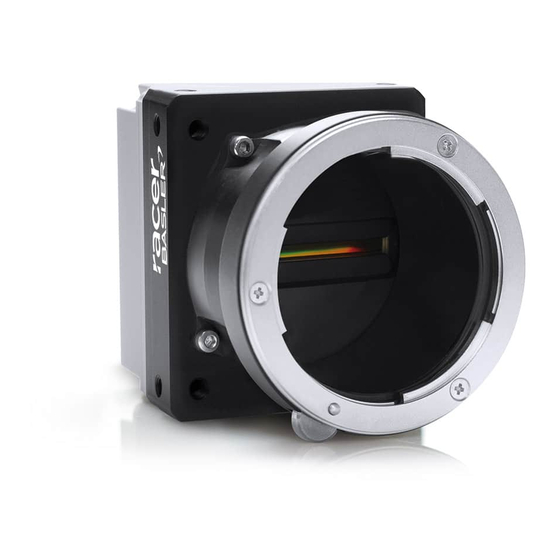
Related Manuals for Basler Racer


Summary of Contents for Basler Racer
- Page 1 Basler racer CAMERA LINK INFORMATION FOR FRAME GRABBER DESIGNERS Document Number: AW001187 Version: 02 Language: 000 (English) Release Date: 1 February 2013 Applies to prototype cameras only. All content is subject to change.
- Page 2 Basler customers using or selling these products for use in such applications do so at their own risk and agree to fully indemnify Basler for any damages resulting from such improper use or sale. Warranty Note Do not open the housing of the camera.
- Page 3 Contacting Basler Support Worldwide Europe: Basler AG An der Strusbek 60 - 62 22926 Ahrensburg Germany Tel.: +49-4102-463-515 Fax.: +49-4102-463-599 support.europe@baslerweb.com Americas: Basler, Inc. 855 Springdale Drive, Suite 203 Exton, PA 19341 U.S.A. Tel.: +1-610-280-0171 Fax.: +1-610-280-7608 support.usa@baslerweb.com Asia: Basler Asia Pte. Ltd.
-
Page 5: Table Of Contents
............39 Basler racer Camera Link... - Page 6 Table of Contents AW00118702000 Basler racer Camera Link...
-
Page 7: Camera Link Implementation
1 Camera Link Implementation 1.1 Overview The Basler racer Camera Link camera transmits Camera Link data in a fashion similar to devices that use National Semiconductor DS90CR287 transmitters. For Camera Link receivers on your frame grabber, we recommend that you use the National Semiconductor DS90CR288A or an equivalent. -
Page 8: Sdr Connector Pin Assignments And Numbering
Two 26-pin, 0.03” pin spacing, Shrunk Delta Ribbon (SDR) female connectors are used on the camera. The pin assignments and pin numbering for the base connector are as shown in Table 2 and for the medium/full connector are as shown in Table 3 on page Basler racer Camera Link... - Page 9 CC4- * Pins 1 and 26 are tied together in the camera. ** Pins 13 and 14 are tied together in the camera. Table 2: Pin Assignments and Numbering for the Base Configuration 26-pin SDR Connector Basler racer Camera Link...
- Page 10 ZClk+ * Pins 1 and 26 are tied together in the camera. ** Pins 13 and 14 are tied together in the camera. Table 3: Pin Assignments and Numbering for the Medium/Full Configuration 26-pin SDR Connector Basler racer Camera Link...
-
Page 11: Electrical Implementation
Camera Link Implementation 1.3 Electrical Implementation The schematics in Fig. 2 through Fig. 6 on the following pages illustrate the basics of the racer Camera Link electrical implementation. The basic difference between the schematics is the number of transmitters used and the port assignments for each transmitter. - Page 12 +12 VDC +12 VDC PoCL In PoCL Out 26-pin Male SDR Connector 26-pin Female SDR Connector +12 VDC In Frame Grabber 6-pin Not Connected Alternative Receptacle Power Not Connected racer Fig. 2: Electrical Implementation - Base Configuration Basler racer Camera Link...
- Page 13 +12 VDC +12 VDC PoCL In PoCL Out 26-pin Male SDR Connector Frame Grabber 26-pin Female SDR Connector +12 VDC In 6-pin Not Connected Alternative Receptacle Power Not Connected racer Fig. 3: Electrical Implementation - Medium Configuration Basler racer Camera Link...
- Page 14 Camera Link Implementation AW00118702000 Fig. 4: Electrical Implementation - Full Configuration (Octo) for 8 bit Pixel Formats Basler racer Camera Link...
- Page 15 AW00118702000 Camera Link Implementation Fig. 5: Electrical Implementation - Full Configuration (Octo) for 10 bit Pixel Formats Basler racer Camera Link...
- Page 16 Camera Link Implementation AW00118702000 Fig. 6: Electrical Implementation - Full Configuration (Deca) Basler racer Camera Link...
-
Page 17: Camera Link Input Signals
ExLSTrig signal is 1 µs and the minimum low time is also 1 µs. The ExLSTrig signal is typically supplied to the camera by the frame grabber board. For details about using a line start trigger with racer cameras, refer to the Basler racer Camera Link User’s Manual (001185xx000). -
Page 18: Camera Link Output Signals
X as shown in Fig. 2, Fig. Fig. Fig. 5, and Fig. transmitter circuit Y as shown in Fig. Fig. Fig. 5, and Fig. transmitter circuit Z as shown in Fig. Fig. 5, and Fig. Basler racer Camera Link... -
Page 19: Data Valid Bit
Geometry setting and also on the bit depth of the pixels being transmitted (bit depth is determined by the current Pixel Format setting). The bit to port assignments for each available combination of tap geometry and pixel format settings are shown in the tables on the following pages. Basler racer Camera Link... -
Page 20: Tap Geometry - 8, 10, Or 12 Bit Pixel Depth
As assigned by user As assigned by user Strobe TxCLKIn RxCLKOut Pixel Clock Pixel Clock Pixel Clock Table 4: Bit Assignments for 1X Tap Geometry – 8, 10, or 12 Bit Pixel Depth (Transmitter Circuit X) Basler racer Camera Link... -
Page 21: 1X2 Tap Geometry - 8, 10, Or 12 Bit Pixel Depth
As assigned by user As assigned by user Strobe TxCLKIn RxCLKOut Pixel Clock Pixel Clock Pixel Clock Table 5: Bit Assignments for 1X2 Tap Geometry – 8, 10, or 12 Bit Pixel Depth (Transmitter Circuit X) Basler racer Camera Link... -
Page 22: 1X4 Tap Geometry - 8, 10, Or 12 Bit Pixel Depth
As assigned by user As assigned by user Strobe TxInCLK RxOutClk Pixel Clock Pixel Clock Pixel Clock Table 6: Bit Assignments for 1X4 Tap Geometry - 8, 10, or 12 Bit Pixel Depth (Transmitter Circuit X) Basler racer Camera Link... - Page 23 TxIn23 RxOut23 Not Used Not Used Not Used Strobe TxInCLK RxOutClk Pixel Clock Pixel Clock Pixel Clock Table 7: Bit Assignments for 1X4 Tap Geometry - 8, 10, or 12 Bit Pixel Depth (Transmitter Circuit Y) Basler racer Camera Link...
-
Page 24: 1X8 Tap Geometry - 8 Or 10 Bit Pixel Depth
Table 8: Bit Assignments for 1X8 Tap Geometry – 8 or 10 Bit Pixel Depth (Transmitter Circuit X) * In 1X8 8 bit mode, this port is DVAL. In 1X8 10 bit mode, DVAL is not present. Instead, this port is I0 and D0 Bit 0 is assigned to it. Basler racer Camera Link... - Page 25 In 1X8 10 bit mode, FVAL is not present. Instead, this port is I2 and D1 Bit 0 is assigned to it. ** In 1X8 8 bit mode, this port is DVAL. In 1X8 10 bit mode, DVAL is not present. Instead, this port is I3 and D1 Bit 1 is assigned to it. Basler racer Camera Link...
- Page 26 In 1X8 10 bit mode, FVAL is not present. Instead, this port is J5 and D6 Bit 1 is assigned to it. ** In 1X8 8 bit mode, this port is DVAL. In 1X8 10 bit mode, DVAL is not present. Instead, this port is J6 and D7 Bit 0 is assigned to it. Basler racer Camera Link...
-
Page 27: 1X10 Tap Geometry - 8 Bit Pixel Depth
Not Used Port D0 TxIn26 RxOut26 D3 Bit 0 Port D1 TxIn27 RxOut27 D3 Bit 1 Strobe TxInCLK RxOutClk Pixel Clock Table 11: Bit Assignments for 1X10 Tap Geometry – 8 Pixel Depth (Transmitter Circuit X) Basler racer Camera Link... - Page 28 RxOut25 D6 Bit 3 Port G4 TxIn26 RxOut26 D6 Bit 4 LVAL TxIn27 RxOut27 Line Valid Strobe TxInCLK RxOutClk Pixel Clock Table 12: Bit Assignments for 1X10 Tap Geometry – 8 Pixel Depth (Transmitter Circuit Y) Basler racer Camera Link...
- Page 29 D9 Bit 6 Port J7 TxIn26 RxOut26 D9 Bit 7 (MSB) LVAL TxIn27 RxOut27 Line Valid Strobe TxInCLK RxOutClk Pixel Clock Table 13: Bit Assignments for 1X10 Tap Geometry – 8 Pixel Depth (Transmitter Circuit Z) Basler racer Camera Link...
- Page 30 Camera Link Implementation AW00118702000 Basler racer Camera Link...
-
Page 31: Pixel Data Output
12 bit format, 12 bits of image data are transmitted for each pixel. 2.2 Pixel Clock Speed The Camera Link pixel clock speed on all racer Camera Link camera models is selectable. The available pixel clock speeds are listed in... -
Page 32: Camera Link Tap Geometries
Pixel Data Output AW00118702000 2.3 Camera Link Tap Geometries All racer Camera Link cameras have a settable Camera Link Tap Geometry parameter. The Camera Link tap geometry setting determines how pixel data will be transmitted via the Camera Link interface. - Page 33 Formula 1: 22.3 µs ------- - x 0.0095 µs 22.319 µs Formula 2: ------- - x 0.015385 µs 0.18462 µs Formula 3: 7 x 0.015385 µs 0.107695 µs Basler racer Camera Link...
-
Page 34: Tap Geometry
8. Transmission according to the 1X tap geometry is shown graphically in Fig. 7 and the timing of pixel data transmission in Fig. Step X = 1 Tap 1 Fig. 7: 1X Tap Geometry Basler racer Camera Link... - Page 35 W = width = the last pixel according to the current image AOI (e.g., the 2048th pixel of the image AOI when the image AOI width is set to 2048). Fig. 8: Timing of Pixel Data Transmission for the 1X Tap Configuration Basler racer Camera Link...
-
Page 36: 1X2 Tap Geometry
Transmission according to the 1X2 tap geometry is shown graphically in Fig. 9 and the timing of pixel data transmission in Fig. Step X = 2 Tap 1 Tap 2 W = width Fig. 9: 1X2 Tap Geometry Basler racer Camera Link... - Page 37 W = width = the last pixel according to the current image AOI (e.g., the 2048th pixel of the image AOI when the image AOI width is set to 2048). Fig. 10: Timing of Pixel Data Transmission for the 1X2 Tap Configuration Basler racer Camera Link...
-
Page 38: 1X4 Tap Geometry
Transmission according to the 1X4 tap geometry is shown graphically in Fig. 11 and the timing of pixel data transmission in Fig. Step X = 4 Tap 1 Tap 2 Tap 3 Tap 4 W = width Fig. 11: 1X4 Tap Geometry Basler racer Camera Link... - Page 39 W = width = the last pixel according to the current image AOI (e.g., the 2048th pixel of the image AOI when the image AOI width is set to 2048). Fig. 12: Timing of Pixel Data Transmission for the 1X4 Tap Configuration Basler racer Camera Link...
-
Page 40: 1X8 Tap Geometry
Fig. Step X = 8 Tap 1 Tap 2 Tap 3 Tap 4 Tap 5 Tap 6 Tap 7 Tap 8 W = width Fig. 13: 1X8 Tap Geometry Basler racer Camera Link... - Page 41 W = width = the last pixel according to the current image AOI (e.g., the 2048th pixel of the image AOI when the image AOI width is set to 2048). Fig. 14: Timing of Pixel Data Transmission for the 1X8 Tap Configuration Basler racer Camera Link...
-
Page 42: 1X10 Tap Geometry
Fig. Step X = 10 Tap 1 Tap 2 Tap 3 Tap 4 Tap 5 Tap 6 Tap 7 Tap 8 Tap 9 Tap 10 W = width Fig. 15: 1X10 Tap Geometry Basler racer Camera Link... - Page 43 W = width = the last pixel according to the current image AOI (e.g., the 2040th pixel of the image AOI when the image AOI width is set to 2040). Fig. 16: Timing of Pixel Data Transmission for the 1X10 Tap Configuration Basler racer Camera Link...
- Page 44 Pixel Data Output AW00118702000 Basler racer Camera Link...
-
Page 45: Revision History
AW00118702000 1 Feb 2013 Initial release of this document applying to series-production status. Updated the e-mail addresses for Basler technical support. Added descriptions of the 1X tap geometry throughout the document. Updated the camera’s back view in Fig. 1 on page Modified the specification for camera power in Table 2. - Page 46 Revision History AW00118702000 Basler racer Camera Link...
Need help?
Do you have a question about the Racer and is the answer not in the manual?
Questions and answers