
Related Manuals for Future Electronics Microsemi Avalanche

Summary of Contents for Future Electronics Microsemi Avalanche
- Page 1 Future Electronics - Microsemi Avalanche Development Board User’s Guide Revision 1.0...
-
Page 2: Table Of Contents
Contents Revision History ..................6 Revision 1.0 ..................6 Getting Started ..................7 Box Contents ..................7 Block Diagram ..................8 Board Overview .................. 8 Powering Up the Board ................ 11 Installation and Setting ................12 Software Settings ................12 Hardware Settings ................ - Page 3 4.10.5 Arduino™ Compatible Expansion Headers ..........23 4.10.6 MikroBUS™ Compatible Expansion Headers ..........24 4.10.7 PMOD™ Compatible Expansion Connector ..........25 Pin List ....................26 Board Component Placement ..............27 Demo Design ..................28 Appendix: Programming PolarFire FPGA Using the On-Board FlashPro5 ..... 29...
- Page 4 Figures Figure 1 - Avalanche Block Diagram ..............8 Figure 2 - Avalanche Board ................9 Figure 3 - Avalanche Board Power Supply Block diagram ..........13 Figure 4 - DDR3 Memory Interface ..............14 Figure 5 - SPI Flash Interface ................15 Figure 6 - XCVR0 Interface ................
- Page 5 Tables Table 1 - Avalanche Board Components ..............10 Table 2 - Power Supply LEDs ................12 Table 3 - I/O Voltage Rails ................12 Table 4 - Wi-Fi LEDs ..................18 Table 5 - User LEDs ..................21 Table 6 - Push-Button Switches ................. 21 Table 7 - J11 SFP+ Connector Pinout ..............
-
Page 6: Revision History
1 Revision History The revision history describes the changes that were implemented in the document. The changes are listed by revision, starting with the most current publication. 1.1 Revision 1.0 Revision 1.0 is the first publication of this document. -
Page 7: Getting Started
2 Getting Started The Future Electronics - Microsemi Avalanche Development Kit (AVMPF300TS-02-NA/EU) is an RoHS-compliant, cost optimized kit with general-purpose interfaces that enables you to evaluate the basic features of the PolarFire family of FPGAs. The Avalanche Development Kit supports the following interfaces: ... -
Page 8: Block Diagram
2.2 Block Diagram The following block diagram shows all the components of the Avalanche Board. Figure 1 - Avalanche Block Diagram 2.3 Board Overview The Avalanche Board features a PolarFire MPF300TS-1FCG484EES FPGA with the following capabilities: 20-Kb dual-port or two-port LSRAM block with a built-in single error correct double error detect (SECDED) capability ... -
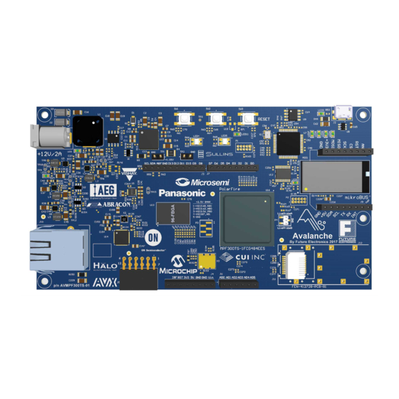
Page 9: Figure 2 - Avalanche Board
The Avalanche Board supports several standard interfaces, including: Microsemi VSC8531 with an RJ45 connector for 10/100/1000 Mbps Ethernet One full-duplex transceiver lane connected through SFP+ connector DDR3 memory 2.4 GHz ISM band using Panasonic PAN9320 Wi-Fi module ... -
Page 10: Table 1 - Avalanche Board Components
The following table lists the important components of the Avalanche Board. Component Label on Board Description Feature Device PolarFire FPGA MPF300TS-1FCG484EES FPGA with data security. Power Supply 12V power supply The board is powered by a 12V power source using an external input 12 V / 2 A DC jack. -
Page 11: Powering Up The Board
2.4 Powering Up the Board The Avalanche Board can only be powered up using the 12 V DC jack. -
Page 12: Installation And Setting
3 Installation and Setting This section provides information about the software and hardware settings required to run the pre-programmed demo design on the Avalanche Board. 3.1 Software Settings Download and install the latest release of Microsemi Libero® SoC PolarFire software from the Microsemi website, and register for a free one-year Gold License to the Libero software. -
Page 13: Figure 3 - Avalanche Board Power Supply Block Diagram
The following figure shows voltage rails (12 V, 5 V, 3.3 V, 2.5 V, 1.8 V, 1.5 V, 1.05 V and 0.9 V) available on the Avalanche Board. Figure 3 - Avalanche Board Power Supply Block diagram... -
Page 14: Board Components And Operations
4 Board Components and Operations This section describes the key components of the Avalanche Board and provides information about important board operations. 4.1 DDR3 Memory Interface One 4-Gb DDR3 SDRAM chip is provided to serve as flexible volatile memory for user applications. -
Page 15: Transceivers
PolarFire FPGA SPI Flash BANK3 (64 Mb) Figure 5 - SPI Flash Interface For more information, see the Board Level Schematics document (provided separately). 4.3 Transceivers The PolarFire MPF300TS-1FCG484EES device has sixteen transceiver lanes, which can be accessed through a PCB loopback and the SPF+ connector on the board. 4.3.1 XCVR0 Interface The XCVR0 interface has two lanes connected as follows: ... -
Page 16: Xcvr1 Interface
4.3.2 XCVR1 Interface The XCVR1 interface has one lane that is connected to the SFP+ connector. The signals are routed in the PCB as follows: Lanes 0 is directly routed to the SFP+ connector. The XCVR0 reference clock can be used with the XCVR1 interface. The following figure shows the XCVR1 interface of the Avalanche Board. -
Page 17: Microsemi Phy (Vsc8531)
4.4 Microsemi PHY (VSC8531) The Microsemi VSC8531 device is designed for space-constrained 10/100/1000BASE-T applications. It features integrated, line-side termination to conserve board space, lower EMI, and improve system performance. Additionally, integrated RGMII timing compensation eliminates the need for on-board delay lines. Microsemi EcoEthernet™... -
Page 18: Panasonic Wi-Fi (Pan9320)
4.5 Panasonic Wi-Fi (PAN9320) The Panasonic PAN9320 is a 2.4 GHz ISM band Wi-Fi-embedded module which includes a wireless radio and an MCU for easy integration of Wi-Fi connectivity into various electronic devices. Figure 10 - PAN9320 Block Diagram The following table shows the different status LEDs of the Wi-Fi Module. Avalanche Board Description Reference... -
Page 19: Microchip Adc (Mcp3903)
4.6 Microchip ADC (MCP3903) The Microchip MCP3903 is a six-channel Analog Front End (AFE) containing three pairs made out of two synchronous sampling Delta-Sigma Analog-to-Digital Converters (ADC) with PGA, a phase delay compensation block, internal voltage reference, and high-speed 10 MHz SPI compatible serial interface. -
Page 20: System Reset
JTAG Port A PolarFire FTDI Mini USB FPGA FT4232 UART Port C EEPROM Figure 13 - FTDI Interface The EEPROM that is connected to the FTDI device is programmed so that Port A of the FTDI device is recognized as an embedded FlashPro5. The FTDI USB to serial device provides four separate interfaces. -
Page 21: User Interface
R1 (GPIO174PB4/CLKIN_W_7/CCC_NW_CLKIN_W_7/CCC_NW_PLL0_OUT0) J3 (GPIO215PB4/CLKIN_W_5/CCC_NW_CLKIN_W_5) The following figure shows the 50-MHz clock oscillator interface PolarFire FPGA 2.5 V 50 MHz Oscillator VSC8531 Figure 15 - 50-MHz Clock Oscillator 4.10 User Interface The Avalanche Board has user LEDs and push-button switches. 4.10.1 User LEDs The Avalanche Board has two dual-color active-high LEDs that are connected to the PolarFire device. -
Page 22: Live Probes Header
4.10.3 Live Probes Header The Avalanche Board provides an header (P4) called Active Probes. Active Probes enable you to read or change the values of probe points in a design through JTAG. The value of probe points may be changed for various reasons, such as: ... -
Page 23: Arduino™ Compatible Expansion Headers
SFP+ Pin Description PolarFire FPGA Bank Number – Pin Number +3.3V Table 7 - J11 SFP+ Connector Pinout 4.10.5 Arduino™ Compatible Expansion Headers The Avalanche Board has an Arduino™ compatible expansion headers to add any Arduino™ compatible interfaces, sensors or devices. For custom applications, I/O pins 4 to 13 can be used in GPIO differential mode providing a 4- bits data bus and a clock signal through connectors J3 and J7. -
Page 24: Mikrobus™ Compatible Expansion Headers
Arduino Pin Description PolarFire FPGA Bank Number – J6 Pin Number AD_CH0 (MCP9303) AD_CH1 (MCP9303) AD_CH2 (MCP9303) AD_CH3 (MCP9303) AD_CH4 (MCP9303) AD_CH5 (MCP9303) Table 10 - J6 Arduino Connector Pinout Arduino Pin Description PolarFire FPGA Bank Number – J7 Pin Number ARD_IO 0 Bank 2 ARD_IO 1... -
Page 25: Pmod™ Compatible Expansion Connector
Mikro Pin Description PolarFire FPGA Bank Number – J9 Pin Number Bank 2 Bank 2 Bank 2 Bank 2 Table 13 - J9 MikroBUS Connector Pinout 4.10.7 PMOD™ Compatible Expansion Connector The Avalanche Board has a PMOD™ compatible expansion connector to add any PMOD™ compatible interfaces, sensors or devices. -
Page 26: Pin List
5 Pin List For information about all package pins on the PolarFire device, see Package Pin Assignment Table. -
Page 27: Board Component Placement
6 Board Component Placement The following figure shows the placement of various components on the Avalanche Board silkscreen. Figure 17 - Silkscreen Top View Figure 18 - Silkscreen Botton View... -
Page 28: Demo Design
7 Demo Design For information about how to run the Out-of-The-Box demo, see the Avalanche Development Board Quick Start Guide provided with your kit. -
Page 29: Appendix: Programming Polarfire Fpga Using The On-Board Flashpro5
6. Click Configure Device. 7. Click Browse, and select the .stp file from the Load Programming File window. Note: The programming file is available through Future Electronics support. 8. From the View Programmer pane, select the on-board FlashPro5 programmer, as shown in the following figure. - Page 30 You acknowledge and agree that the reference designs and other such design materials included herein are provided as an example only and that you will exercise your own independent analysis and judgment in your use of these materials. Future Electronics assumes no liability for your use of these materials for your product designs.
Need help?
Do you have a question about the Microsemi Avalanche and is the answer not in the manual?
Questions and answers