Sign In
Upload
Download
Table of Contents
Contents
Add to my manuals
Delete from my manuals
Share
URL of this page:
HTML Link:
Bookmark this page
Add
Manual will be automatically added to "My Manuals"
Print this page
×
Bookmark added
×
Added to my manuals
Manuals
Brands
Atari Manuals
Desktop
520STE
Field service manual
Atari 520STE Field Service Manual
Hide thumbs
1
2
Table Of Contents
3
4
5
6
7
8
9
10
11
12
13
14
15
16
17
18
19
20
21
22
23
24
25
26
27
28
29
30
31
32
33
34
35
36
37
38
39
40
41
42
43
44
45
46
47
48
49
50
51
52
53
54
55
56
57
58
59
60
61
62
63
64
65
66
67
68
69
70
71
72
73
74
75
76
77
78
79
80
81
page
of
81
Go
/
81
Contents
Table of Contents
Troubleshooting
Bookmarks
Table of Contents
Table of Contents
1 Overview
Case Design
Main Components
Section One: Introduction
Negative Supplies
Power Supply
Section Two. Theory of Operation
2 Overview
Audio/Video Subsystem
Main System
Gstmcu
Inputloutput Subsystems
Microprocessing Unit
Main Memory
Direct Memory Access
Multi-Function Peripheral Control
Audio/Viideo Subsystem
Digitized Sound
Genlock and the STE
Input/Output Subsystems
System Startup
System Errors
Section Three: Testing
Overview
Test Configuration
Troubleshooting a Dead Unit
Diagnostic Cartridge
Power up Sequence
Test Menu
RAM Test
ROM Test
Color Test
Keyboard Test
MIDI Tests
RS232 Tests
Audio Test
Timing Tests
DMA Tests
Fioppy Disk Tests
Printer and Joystick Port Tests
Monochrome Monitor
Hard Disk Writeiread
Graphics Chip Blit
Error Codes Quick Reference
Section Four: Disassembly/Assembly
STE Disassembly
STE Reassembly
Section Five: Symptom Checklist
Display Problems
Disk Drive Problems
Keyboard Problems
MIDI Problems
RS232 Problems
Printer Port Problems
Hard Disk Port Problems
DMA Sound
Section Six: Diagnostic Flowcharts
Replacement Procedures
Handling of Integrated Circuits
Section Seven: Parts List
Section Eight: Glossary
Section Nine: Schematics and Silkscreens
Advertisement
Quick Links
1
Ste Disassembly
2
Section Nine: Schematics and Silkscreens
Download this manual
Table of
Contents
Previous
Page
Next
Page
1
2
3
4
5
Advertisement
Table of Contents
Need help?
Do you have a question about the 520STE and is the answer not in the manual?
Ask a question
Questions and answers
Related Manuals for Atari 520STE
Desktop Atari 520ST Owner's Manual
(84 pages)
Desktop Atari 520ST Owner's Manual
512 different colors, three graphics modes, 80 columns of text, enhanced graphics resolution (84 pages)
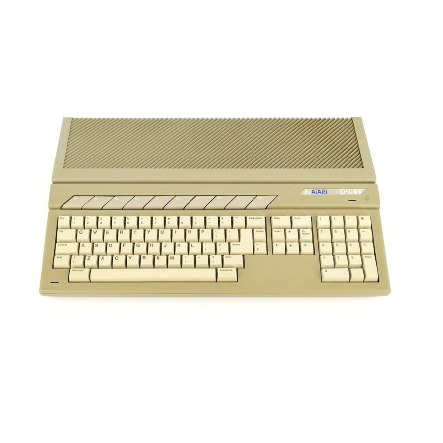
Desktop Atari 1040STE Field Service Manual
(81 pages)
Desktop Atari 800 Owner's Manual
Home computer (20 pages)
Desktop Atari MEGA STe Owner's Manual
(93 pages)
Desktop Atari 65XE Owner's Manual
(135 pages)
Desktop Atari 400 User Manual
(244 pages)
Desktop Atari Faicon030 Owner's Manual
32-bit computer (196 pages)
Desktop Atari 400 User Manual
(84 pages)
Desktop Atari 130XE Owner's Manual
(143 pages)
Desktop Atari 1200 XL Field Service Manual
(51 pages)
Desktop Atari ST Owner's Manual
(99 pages)
Desktop Atari ST series Technical Reference Manual
(420 pages)
Desktop Atari STACY Owner's Manual
(16 pages)
Desktop Atari 1200 XL Owner's Manual
Home computer (20 pages)
Desktop Atari Mega 2 Manual
(90 pages)
This manual is also suitable for:
1040ste
Table of Contents
Save PDF
Print
Rename the bookmark
Delete bookmark?
Delete from my manuals?
Login
Sign In
OR
Sign in with Facebook
Sign in with Google
Upload manual
Upload from disk
Upload from URL


Need help?
Do you have a question about the 520STE and is the answer not in the manual?
Questions and answers