
Related Manuals for Nokia NPL-3 Series


Summary of Contents for Nokia NPL-3 Series
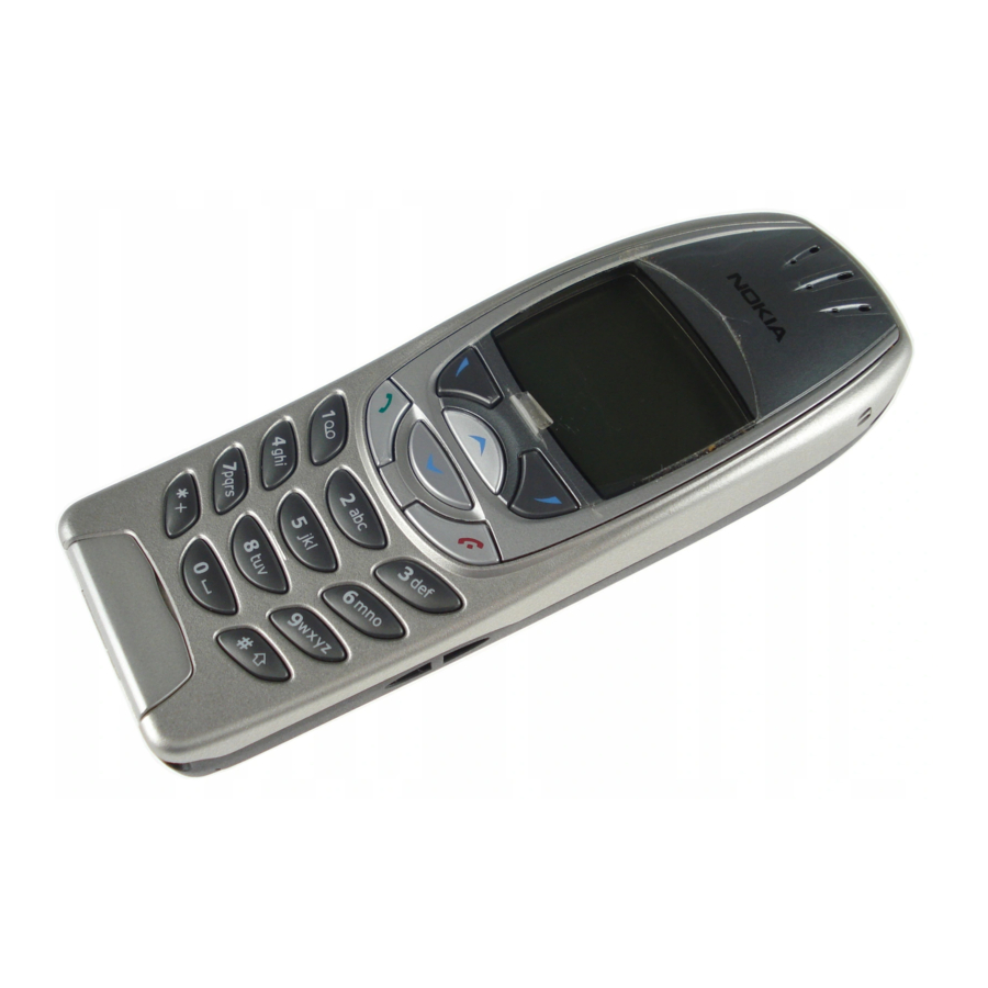
- Page 1 Customer Care Solutions NPL-3 Series Transceivers Troubleshooting Instructions Issue 1 3/03 ãNokia Corporation...
-
Page 2: Table Of Contents
Illumination fault .......................42 Charger Fault ......................43 Accessory Fault ......................44 Audio Fault ........................45 FM Radio troubleshooting ...................49 FM Radio component layout ..................49 FM Radio troubleshooting diagram ................50 Notes to "FM Radio troubleshooting diagram" ............50 ãNokia Corporation. Page 2 Issue 1 3/03... -
Page 3: Rf Troubleshooting
When using RF probe usually a good way is to use metallic tweezers to connect probe ground to PWB ground as close to measurement point as pos- sible. ãNokia Corporation. Issue 1 3/03 Page 3... -
Page 4: Rf Key Component Placement
Company confidential Troubleshooting Instructions CCS Technical Documentation RF Key component placement Figure 1: Component placement 1 GSM850_TX Antenna switch Balanced saw GSM1900_RX GSM1800/1900 TX GSM1900 LNA Balun GSM1900_RX balun Helgo VCTCXO VCO balun ãNokia Corporation. Page 4 Issue 1 3/03... -
Page 5: Rf Measurement Points
To antenna ASM_In_TX1800_1900 850PA_IN ASM_out_850RX ASM_out_1800RX VTXB850 ASM_out_1900RX VPCTRL_850 VANT_3 VPCTRL_1800_1900 RX_saw_out VTXB_1800_1900 VBATT LNA_VCC 1800_1900PA_IN LNA_P VPECTRL3 (ALC) 1900_RX_In 1800_RX_In RFBusReset 850_RX_In RFBusData RFBusEn RFBusClk VCTCXO 26Mhz out 26MHz to BB TXIN/TXIP TXQP/QN ãNokia Corporation. Issue 1 3/03 Page 5... -
Page 6: Gsm850, Gsm1800 & Gsm1900 Transmitter
- Select band "GSM850" or "GSM 1800" or "GSM1900" (Default = "GSM850") - Set Active unit to "Tx" (Default = "Rx") - Set Operation mode to "Burst" (Default = "Burst") - Set Tx data type to "Random" (Default = "All1") ãNokia Corporation. Page 6 Issue 1 3/03... - Page 7 - Set Rx/Tx channel to 190 on GSM850 band or 700 on GSM1800 band or 661 on GSM1900 (Defaults) - Set Tx PA mode to "Free" (Default) - Set power level to 5 (Default = 19) on GSM850 or to 0 (Default = 15) on GSM1800 or GSM1900 ãNokia Corporation. Issue 1 3/03 Page 7...
-
Page 8: Transmitter Troubleshooting Diagram
NPL-3 Company confidential Troubleshooting Instructions CCS Technical Documentation Transmitter troubleshooting diagram Figure 3: Transmitter troubleshooting ãNokia Corporation. Page 8 Issue 1 3/03... - Page 9 Company confidential NPL-3 CCS Technical Documentation Troubleshooting Instructions Figure 4: HELGO IC troubleshooting ãNokia Corporation. Issue 1 3/03 Page 9...
- Page 10 NPL-3 Company confidential Troubleshooting Instructions CCS Technical Documentation Figure 5: PA and Antenna Switch troubleshooting ãNokia Corporation. Page 10 Issue 1 3/03...
-
Page 11: Pictures Of Transmitter Signals
VANT_2 / GSM1800 TX at R808 VANT_3 / GSM1900 TX at C805 OV ( no signal/ Flatline on Oscilloscope screen) 500mV/div MTB 100us/div 500mV/div 100us/div VTXB_850 at C713 TXP at J504 VTXB_1800_1900 at C714 ãNokia Corporation. Issue 1 3/03 Page 11... - Page 12 NPL-3 Company confidential Troubleshooting Instructions CCS Technical Documentation Figure 7: Tx out signal, 850 band, burst mode, channel 190 ãNokia Corporation. Page 12 Issue 1 3/03...
-
Page 13: Additional Information For Edge Troubleshooting
Set power level to 8 (Default = 19) on GSM850 or to 2 (Default = 0) on GSM1800 or GSM1900 NOTE! For GSM850 Edge power levels 5, 6 and 7 are not in use and for GSM1800&1900 Edge power levels 0 and 1 are not in use. ãNokia Corporation. Issue 1 3/03 Page 13... - Page 14 NPL-3 Company confidential Troubleshooting Instructions CCS Technical Documentation Figure 8: Transmitter EDGE troubleshooting ãNokia Corporation. Page 14 Issue 1 3/03...
- Page 15 Company confidential NPL-3 CCS Technical Documentation Troubleshooting Instructions Figure 9: Helgo EDGE troubleshooting ãNokia Corporation. Issue 1 3/03 Page 15...
- Page 16 NPL-3 Company confidential Troubleshooting Instructions CCS Technical Documentation Figure 10: Pa & ant switch EDGE troubleshooting ãNokia Corporation. Page 16 Issue 1 3/03...
-
Page 17: Pictures Of Edge Transmitter Signals
Company confidential NPL-3 CCS Technical Documentation Troubleshooting Instructions Pictures of EDGE transmitter signals Figure 11: I_ref_850 power level 8 at R701/C701 Figure 12: VTXB 850 power level 8 at C713 ãNokia Corporation. Issue 1 3/03 Page 17... - Page 18 NPL-3 Company confidential Troubleshooting Instructions CCS Technical Documentation Figure 13: I_ref_1800/1900 power level 2 at R700/C700 Figure 14: VTXB 1800/1900 power level 2 at C714 ãNokia Corporation. Page 18 Issue 1 3/03...
- Page 19 Company confidential NPL-3 CCS Technical Documentation Troubleshooting Instructions Figure 15: TXA 850/1800/1900 at C538 Figure 16: TXI/TXQ signal at C535/C536/R516/R517 ãNokia Corporation. Issue 1 3/03 Page 19...
- Page 20 NPL-3 Company confidential Troubleshooting Instructions CCS Technical Documentation Figure 17: VPECTRL3 (ALC) signal at C512 ãNokia Corporation. Page 20 Issue 1 3/03...
-
Page 21: Gsm850, Gsm1800 And Gsm1900 Receiver
For continuous mode: - Set Operation mode to "Continuous" - Set AGC to "12: FEG_ON + DTOS_ON + BB_30=Vgain60” (maximum gain setting used in normal mode) (Default = "14: FEG_ON + DTOS_ON + BB_42=Vgain72") ãNokia Corporation. Issue 1 3/03 Page 21... - Page 22 (channel 190) measured from testpoint RXI or RXQ with 881.6671 MHz signal, input level –90dBm at RF-connector. Correct signal amplitudes approximately: • GSM850~170mVpp • GSM1800~140mVpp • GSM1900~160mVpp Signal part frequency 67.7kHz sine. ãNokia Corporation. Page 22 Issue 1 3/03...
- Page 23 Trace2: With wider time scaling both monitoring and own RX bursts are seen, 1 burst (shorter) is monitoring and 2 burst (longer) is own RX burst. Trace1: External LNA VCC supply voltage at burst mode, input level –90 dBm. Measured from testpoint LNA_VCC. ãNokia Corporation. Issue 1 3/03 Page 23...
- Page 24 RXI and RXQ simultaneously. Used channel 190, input signal 881.6671 MHz, level –90 dBm at antenna port, AGC set- ting 12. Phase difference should be 90 degrees between RX I and Q signals at all bands. ãNokia Corporation. Page 24 Issue 1 3/03...
-
Page 25: Troubleshooting Diagram For Gsm850 Receiver
* ** DC–level of RXI/RXQ in Spectrumanalyzer continuous mode will decrease 4G VCO out Synthesiszer trou- slowly. 3769.6MHz bleshooting The original level can be resto- ∼–30 dBm (* red by rewriting gain set. Check HELGA N500 ãNokia Corporation. Issue 1 3/03 Page 25... -
Page 26: Troubleshooting Diagram For Gsm1800 Receiver
4G VCO out Synthesiszer trou- * ** DC–level of RXI/RXQ in 3769.6MHz bleshooting continuous mode will decrease ∼–30 dBm (* slowly. The original level can be resto- red by rewriting gain set. Check HELGA N500 ãNokia Corporation. Page 26 Issue 1 3/03... -
Page 27: Troubleshooting Diagram For Gsm1900 Receiver
4G VCO out Synthesiszer trou- 3685.6MHz bleshooting * ** DC–level of RXI/RXQ in ∼–30 dBm (* continuous mode will decrease slowly. The original level can be resto- red by rewriting gain set. Check HELGA N500 ãNokia Corporation. Issue 1 3/03 Page 27... -
Page 28: Synthesizer
- Set Active unit to "Rx" (Default = "Rx") - Set Operation mode to "Continuous" (Default = "Burst") - Set Rx/Tx channel to 190 on GSM850 band, 700 on GSM1800 band, 661 on GSM1900 band (Defaults) ãNokia Corporation. Page 28 Issue 1 3/03... - Page 29 VCO pin solder joints 0V ? OK ? Replace faulty component(s) Check with oscilloscope: Check VCO control VCO control voltage loop components from VCO pin OK ? >4.0 V ? Replace ãNokia Corporation. Issue 1 3/03 Page 29...
-
Page 30: Pictures Of Synthesizer Signals
NPL-3 Company confidential Troubleshooting Instructions CCS Technical Documentation Pictures of synthesizer signals Figure 25: 26MHz at G501 pin out Figure 26: 26MHz RFCLK at R420/C420 Figure 27: 1800 TX, channel 512, burst mode ãNokia Corporation. Page 30 Issue 1 3/03... - Page 31 34.0 d B R B W 10 kH z VB W 10 kH z SW P 50 m s C EN TER 3. 685600 G H z SPA N 1. 000 M H z ãNokia Corporation. Issue 1 3/03 Page 31...
-
Page 32: Baseband Troubleshooting
J408 CBUSENX (UPP->UEM) J411 FBUSTX (UPP->UEM) VFLASH1 (C205) J409 MBUSTX (UPP->UEM) J410 MBUSRX (UEM->UPP) J412 FBUSRX (UEM->UPP) J386 SIMIODAO (UEM<>SIM) SleepClk crystal (C209, VSIM (C203) J153 CLK (UPP->AUDIO J152 ENB (UPP->AUDIO MICB1 (C152) ãNokia Corporation. Page 32 Issue 1 3/03... -
Page 33: Main Troubleshooting Diagram
Phone doesn’t read SIM card SIM card fault Audios doesn´t work Audio faults Keypad Keypad doesn´t work faults Display Display doesn´t work faults Accessory Accessory doesn´t work faults Illuminationy Illumination doesn't work faults ãNokia Corporation. Issue 1 3/03 Page 33... -
Page 34: Phone Is Dead
< 50 mA jammed working OK? Flash fault Phone current ~54 mA Check BSI-line including Is phone in Change UEM X100,C100,C240,R202 LOCAL mode ? and R206. Are they OK? Change defect part ãNokia Corporation. Page 34 Issue 1 3/03... -
Page 35: Flash Programming Fault
LOW after it has been HIGH? Wrong Change Flash manufactor ID and device ID Is phone totally Phone is dead dead? Phone doesn't Phone is start up or it's jammed jammed? End (retest) ãNokia Corporation. Issue 1 3/03 Page 35... -
Page 36: Phone Is Jammed
Is it OK ? If OK change G501 Is it OK ? Check R420, C420. If OK change N500 Measure PURX signal from testpoint J402. Change UEM Is it HIGH (~1.8V) ? Phone is jammed ãNokia Corporation. Page 36 Issue 1 3/03... - Page 37 Is it OK ? read from testpoint J412. Is it OK ? Measure FBUSTx Change signal during phone info read from testpoint J411. Is it OK ? Change wv8 Change module or retest ãNokia Corporation. Issue 1 3/03 Page 37...
-
Page 38: Sim Card Fault (Insert Sim / Card Rejected)
X386. Is it ~3.0V? If OK, change R388. If still fail, change UEM. Check SIM lines (X386). If Check SIM power-up OK, change R388. If still fail, sequence. Is it OK? change UEM. Change UPP ãNokia Corporation. Page 38 Issue 1 3/03... -
Page 39: Keypad Fault
FAIL, change working? Is it ~1.8V? Measure COL0 Check S301 and from S301 when COL0 line. If OK, pressed. Is there change Z300.If still 50us pulse? FAIL, change UPP Continue Change UPP ãNokia Corporation. Issue 1 3/03 Page 39... - Page 40 J403 when ROW4 from X301. key is pressed. If OK, change Z300. If still fails, change UPP Is voltage level ~1.8V? When keypad is pressed, are the LED's turned on? Illumination fault ãNokia Corporation. Page 40 Issue 1 3/03...
-
Page 41: Display Fault
Measure SDA (J305) R308,R309 and and SCLK (J307) lines. If OK, signals. Are voltage change UPP. levels ~1.8V? Are the display LED's Illumination working when key is fault pressed or enabled by Phoenix SW? ãNokia Corporation. Issue 1 3/03 Page 41... -
Page 42: Illumination Fault
Check N300, L300, V300, R300,C303,C304. ~7.5V when LED driver is If not OK, change defect part. enabled. Is it OK? Check all LED's in UI PWB Change defect parts (V101 - V106). Are they OK? Retest ãNokia Corporation. Page 42 Issue 1 3/03... -
Page 43: Charger Fault
Is it ~25C? Change defect part, re-calibrate and retest. Measure charger Check R200. Is it current throug F100. Change UEM Is it ~350...390mA (with ACP-7)? Change defect part, re-calibrate charge current/voltage. Retest. Retest ãNokia Corporation. Issue 1 3/03 Page 43... -
Page 44: Accessory Fault
(pin3). Is it ~0V? If not OK, change defect part and retest. Measure VOUT Check that regulator N100 enable-pin is voltage (pin4). LOW-state. Is it ~0V? If not OK, check ACI-line again Retest ãNokia Corporation. Page 44 Issue 1 3/03... -
Page 45: Audio Fault
If OK change UEM ~1.38V ? Measure Check L102, C116, MICB2 voltage from C150, R153, C159, XMICP (L102 input). R158 and line. Is it ~2.1V ? If OK change UEM. Audio faults Earpiece ãNokia Corporation. Issue 1 3/03 Page 45... - Page 46 Check C154. If OK signal to UEM (R155). pads (J310,J311). change UEM Is it ~130mVpp ? Is It ~880mVpp ? Check C154, R155, C156, R154, C159, R158, R159 and lines. Change UPP Retest ãNokia Corporation. Page 46 Issue 1 3/03...
- Page 47 C152, C153, R156, voltage from MICP pad. R157. Is it ~2.1V ? If OK change UEM Check C151, R157, C153 and line. If OK change UEM if still fail change UPP Audio faults ãNokia Corporation. Issue 1 3/03 Page 47...
- Page 48 Check signal in C161. C169, C170, Is it OK ? R170, C171. If OK then change UEM Check IHF PA Change IHF controls on J152, PA (N150) J153, J154. Is it OK ? Change UPP ãNokia Corporation. Page 48 Issue 1 3/03...
-
Page 49: Fm Radio Troubleshooting
Company confidential NPL-3 CCS Technical Documentation Troubleshooting Instructions FM Radio troubleshooting FM Radio component layout Figure 47: Component placement Figure 48: Trace layout. ãNokia Corporation. Issue 1 3/03 Page 49... -
Page 50: Fm Radio Troubleshooting Diagram
- Amplitude, A, –67.0 dBm - Carrier frequency, f , 98,000 MHz - Deviation, ,f, 75 kHz - Modulating frequency f , 1,000 kHz (RF generator internal) - FM stereo, mode R=L, pilot state ON ãNokia Corporation. Page 50 Issue 1 3/03... - Page 51 87.5 and 108.0 MHz. Measure audio from C162 and C163. Both OK ? Change N356. Measure signal from J103 and J104. Is it OK ? E Nokia Corporation Change OK, RETEST IN FLALI radio module TB4 ãNokia Corporation. Issue 1 3/03 Page 51...
- Page 52 Signal 2: Audio output from FM radio pins 22 and 23(same as in C162 and C163), with FM test signa Figure 52: FM radio clock from test point J359, 32 kHz frequency clock signal, when radio is on.l ãNokia Corporation. Page 52 Issue 1 3/03...
- Page 53 MEAS UNCAL CONT SGL FREE RUN VIDEO LINE WA SB EXTERNAL CORR SC FS SYNC CRD CENTER 196.450 MHz SPAN 1.000 MHz TV TRIG #RES BW 10 kHz #VBW 10 kHz #SWP 20.0 msec ãNokia Corporation. Issue 1 3/03 Page 53...
- Page 54 NPL-3 Company confidential Troubleshooting Instructions CCS Technical Documentation This page left blank intentionally. ãNokia Corporation. Page 54 Issue 1 3/03...
Need help?
Do you have a question about the NPL-3 Series and is the answer not in the manual?
Questions and answers