Table of Contents
Advertisement
SERVICE MANUAL
Ver. 1.0 2010.04
CD player section
System
Compact disc digital audio system
Laser diode properties
Emission duration: Continuous
Laser output: Less than 44.6 μW
(This output is the value measured at a distance of
about 200 mm from the objective lens surface on the
optical pick-up block with 7 mm aperture.)
Number of channels
2
Frequency response
20 Hz - 20,000 Hz +1/–2 dB
Wow and fl utter
Below measurable limit
Radio section
Frequency range
FM: 87.5 MHz - 108 MHz
CND, E92, MX model:
AM: 530 - 1,710 kHz
AEP, AUS, CET, IT, TH, TW model:
AM: 531 - 1,602 kHz
E41, AR, SP model:
AM: 531 kHz - 1,602 kHz (9 kHz step)
530 kHz - 1,610 kHz (10 kHz step)
Sony Corporation
9-889-823-01
2010D04-1
Audio&Video Business Group
©
2010.04
Published by Sony Techno Create Corporation
CFD-S07CP
Model Name Using Similar Mechanism
CD
Section
Optical Pick-up Name
Model Name Using Similar Mechanism
TC
Section
Tape Transport Mechanism Type
SPECIFICATIONS
IF (AEP, AUS, CET, IT, TH model)
FM: 128 kHz
AM: 45 kHz
Antennas
FM: Telescopic antenna
AM: Built-in ferrite bar antenna
Cassette-corder section
Recording system
4-track 2 channel stereo
Fast winding time
Approx. 150 s (sec.) with Sony cassette C-60
Frequency response
TYPE I (normal): 80 Hz - 10,000 Hz
General
Speaker
Full range: 8 cm (3
Outputs
Headphones jack (stereo minijack):
For 16 Ω - 32 Ω impedance headphones
Input
AUDIO IN jack (stereo minijack)
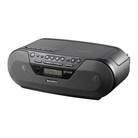
CD RADIO CASSETTE-CORDER
Canadian Model
AEP Model
E Model
Australian Model
CFD-S05
DA11MMVGP
CFD-S05
MF-S05V/S05VE
inches) dia., 4 Ω, cone type (2)
1/4
– Continued on next page –
Advertisement
Table of Contents

Related Manuals for Sony CFD-S07CP


Summary of Contents for Sony CFD-S07CP
- Page 1 7 mm aperture.) Number of channels 4-track 2 channel stereo Fast winding time Approx. 150 s (sec.) with Sony cassette C-60 Frequency response 20 Hz - 20,000 Hz +1/–2 dB Frequency response Wow and fl utter...
- Page 2 LES DIAGRAMMES SCHÉMATIQUES ET LA LISTE DES PIÈCES SONT CRITIQUES POUR LA SÉCURITÉ DE FONC- TIONNEMENT. NE REMPLACER CES COMPOSANTS QUE PAR DES PIÈCES SONY DONT LES NUMÉROS SONT DON- NÉS DANS CE MANUEL OU DANS LES SUPPLÉMENTS PUBLIÉS PAR SONY.
-
Page 3: Table Of Contents
CFD-S07CP UNLEADED SOLDER TABLE OF CONTENTS Boards requiring use of unleaded solder are printed with the lead- free mark (LF) indicating the solder contains no lead. SERVICING NOTES ..........(Caution: Some printed circuit boards may not come printed with the lead free mark due to their particular size) DISASSEMBLY 2-1. -
Page 4: Servicing Notes
CFD-S07CP SECTION 1 SERVICING NOTES PRECAUTION WHEN INSTALLING A NEW OP UNIT/ CHUCK PLATE JIG ON REPAIRING PRECAUTION BEFORE UNSOLDERING THE STATIC ELECTRICITY PREVENTION SOLDER BRIDGE On repairing CD section, playing a disc without the lid (CD), use Chuck Plate Jig. -
Page 5: Disassembly
CFD-S07CP SECTION 2 DISASSEMBLY • This set can be disassembled in the order shown below. 2-1. CABINET (UPPER) SECTION (Page 6) 2-2. CABINET (FRONT) SECTION 2-5. CD BLOCK ASSY (Page 6) (Page 8) 2-10. KEY BOARD 2-6. MOTOR BOARD (Page 10) (Page 8) 2-3. -
Page 6: Cabinet (Upper) Section
CFD-S07CP Note: Follow the disassembly procedure in the numerical order given. 2-1. CABINET (UPPER) SECTION 5 screw (+BV tapping (B2.6)) 4 two screws (+BV tapping (B2.6)) 3 six screws qs cabinet (upper) section (+BV tapping (B2.6)) 1 battery case lid... -
Page 7: Main Board
CFD-S07CP 2-3. MAIN BOARD 2 CN1 (2P) 1 CN901 (3P) 4 three screws (+P tapping (B2.6)) 3 three screws (+P tapping (B2.6)) 5 MAIN board cabinet (rear) section 2-4. POWER BOARD 1 CN901 (3P) 3 screw (+BV tapping (B2.6)) 6 CN903 (2P) -
Page 8: Cd Block Assy
CFD-S07CP 2-5. CD BLOCK ASSY 6 CD block assy 4 two vibration proof rubbers (red) 1 four screws (+PWH tapping (B2.6)) 3 two vibration proof rubbers (green) 5 CD cover cabinet (upper) section 2-6. MOTOR BOARD 1 Remove the four solders. -
Page 9: Cd Lid
CFD-S07CP 2-7. CD LID 7 CD lid cabinet (upper) section 2 damper 1 screw (+BV tapping (B2.6)) 2-8. MD BLOCK ASSY 3 three screws (+BV tapping (B2.6)) 1 screw 4 MD block assy (+BV tapping (B2.6)) 2 SWITCH board cabinet (upper) section... -
Page 10: Cassette Lid
CFD-S07CP 2-9. CASSETTE LID 6 cassette lid cabinet (upper) section 2 damper 1 screw (+BV tapping (B2.6)) 2-10. KEY BOARD 2 screw (+BV tapping (B2.6)) 1 two screws (+BV tapping (B2.6)) 8 KEY board 5 JACK board 6 four screws... -
Page 11: Mechanical Adjustments
CFD-S07CP SECTION 3 SECTION 4 MECHANICAL ADJUSTMENTS ELECTRICAL ADJUSTMENTS Precaution TAPE SECTION 0 dB = 0.775V 1. Clean the following parts with a denatured-alcohol-moistened • Standard Output Level swab: record/playback head pinch roller Output terminal HP OUT erase head rubber belts 32 Ω... -
Page 12: Tuner Section
CFD-S07CP Record/Playback Head Azimuth Adjustment TUNER SECTION 0 dB = 1 μV Procedure: • AM Section Mode: playback Setting: RADIO BAND•AUTO PRESET button: AM test tape Audio level meter P-4-A063 AM RF signal (6.3 kHz, –10 dB) generator Put the lead-wire antenna close to the set. -
Page 13: Cd Section
CFD-S07CP CD SECTION CD section adjustments are done automatically in this set. In case of operation check, confi rm that focus bias. FOCUS BIAS CHECK 1. Connect the oscilloscope between IC801 pin ul and pin ik (or TP804 (RF) and TP711 (VREF)). - Page 14 CFD-S07CP MEMO...
-
Page 15: Diagrams
CFD-S07CP SECTION 5 DIAGRAMS 5-1. BLOCK DIAGRAM – CD Section – CD- L 1-bit DAC DIGITAL EQUALIZER, FNI1 (A) MAIN EFM DECODE, DSP SECTION CD-R (Page 16) FPI1 (B) FNI2 (C) RF AMP & FPI2 (D) TNI (E) CD RF AMP/SERVO CONTROL,... -
Page 16: Block Diagram -Main Section
CFD-S07CP 5-2. BLOCK DIAGRAM – MAIN Section – ANT1 INPUT SELECT, BROADCAST FM TELESCOPIC ELECTRONIC VOLUME, FM/AM RADIO ANTENNA TREBLE/BASS CONTROL RECEIVER IC303 IN L TU LOUT R-CH ROUT R-CH J302 FERRITE-BAR AUDIO IN SDIO RCLK SDIO ANTENNA SCLK SCLK... - Page 17 CFD-S07CP THIS NOTE IS COMMON FOR PRINTED WIRING BOARDS AND SCHEMATIC DIAGRAMS. • Circuit Boards Location (In addition to this, the necessary note is printed in each block.) For Printed Wiring Boards. For Schematic Diagrams. SWITCH board Note: Note: • All capacitors are in μF unless otherwise noted. (p: pF) 50 •...
-
Page 18: Printed Wiring Board -Main Section
CFD-S07CP 5-3. PRINTED WIRING BOARD – MAIN Section – • See page 17 for Circuit Boards Location. • : Uses unleaded solder. J301 ANT1 MAIN BOARD FM TELESCOPIC ANTENNA SP201 C243 SPEAKER (R-CH) SP101 CN301 SPEAKER JW146 AM FERRITE BAR ANTENNA... -
Page 19: Printed Wiring Boards -Key, Power Section
CFD-S07CP 5-4. PRINTED WIRING BOARDS – KEY, POWER Section – • See page 17 for Circuit Boards Location. • : Uses unleaded solder. (Page 18) MAIN BOARD CN310 KEY BOARD JACK BOARD S401 VOLUME VOLUME AUDIO IN RADIO BAND/ TAPE... -
Page 20: Schematic Diagram -Main Section (1/3)
CFD-S07CP 5-5. SCHEMATIC DIAGRAM – MAIN Section (1/3) – • See page 17 for waveforms. • See page 25, 26 for IC Block Diagrams. • See page 28 for IC Pin Function Description of IC801. LCD401 R892 R967 R994 R993... -
Page 21: Schematic Diagram -Main Section (2/3)
CFD-S07CP 5-6. SCHEMATIC DIAGRAM – MAIN Section (2/3) – • See page 17 for waveforms. • See page 26 for IC Block Diagram. (Page 20) (Page 22) IC B/D IC301 C330 C102 R103 R104 R102 C301 C103 R301 FB201 C104... -
Page 22: Schematic Diagram -Main Section (3/3)
CFD-S07CP 5-7. SCHEMATIC DIAGRAM – MAIN Section (3/3) – • See page 27 for IC Block Diagrams. CN313 CN312 R426 C964 C959 C963 L811 C404 C405 C408 R424 R423 R414 IC401 IC807 C409 R420 C220 R223 R224 R225 C120 R123... -
Page 23: Schematic Diagram -Key Section
CFD-S07CP 5-8. SCHEMATIC DIAGRAM – KEY Section – S401 R411 R413 R415 R416 R417 R418 R419 W401 S409 S408 S407 S406 S405 S404 S403 S402 (Page 20) S416 S415 S414 S413 S412 S411 S410 R408 R406 R405 R404 R403 R401... -
Page 24: Schematic Diagram -Power Section
CFD-S07CP 5-9. SCHEMATIC DIAGRAM – POWER Section – J901 FH904 FH903 CN903 F902 F901 FH902 FH901 C901 D901 D903 C903 JW902 C905 T901 C902 D902 D904 C904 C906 CN902 (Page 22) CFD-S07CP... - Page 25 CFD-S07CP • IC Block Diagrams IC1 SI4730-C40 (MAIN Board (1/3)) DOUT GPIO2/DCLK GPIO2/INT GPIO1 LOW-IF LOUT ROUT RFGND CONTROL / INTERFACE RCLK SDIO SCLK IC701 BA5826HFP-E2 (MAIN Board (1/3)) SP– D.BUFF F– D.BUFF LEVEL D.BUFF SHIFT D.BUFF SPIN LEVEL SHIFT...
- Page 26 CFD-S07CP IC803 S-T111B15MC-OGATFG (MAIN Board (1/3)) IC804 S-T111B15MC-OGATFG (MAIN Board (1/3)) 5 VIN ON/OFF CONTROL OVERCURRENT PROTECTOR 4 VOUT REFERENCE VOLTAGE CIRCUIT IC301 TA2068NG (MAIN Board (2/3)) LINE L.LIN L.PO MIC I/EX AMP1 TAPE BUF AMP L.NF RADIO L.RAD AMP1 L.RO...
- Page 27 CFD-S07CP IC302 UTC8227S (MAIN Board (3/3)) IC303 BD3491FS-SE2 (MAIN Board (3/3)) VCC/2 I2C BUS LOGIC SURROUND TREBLE/BASS INPUT GAIN INPUT SELECTOR VOLUME VOLUME 15 16...
- Page 28 CFD-S07CP • IC Pin Function Description MAIN BOARD (1/3) IC801 TC94A77FG-717 (CD-RF AMP/SERVO CONTROL, AUDIO DAC, DSP, LCD DRIVER, SYSTEM CONTROL) Pin No. Pin Name Description Feed (Sled) servo equalizer signal output Disc (spindle) servo equalizer signal output KEY1-I Key signal input...
- Page 29 CFD-S07CP Pin No. Pin Name Description — Not used (Open) VDDM1 — Power supply (Memory VDD+1.5V) HOLD Hold input — Ground VDD1 — Power supply (VDD+1.5V) EFM and PLCK phase deference signal output TMAX TMAX detection result output LPFN PLL circuit LPF amplifi er inversion input LPFO PLL circuit LPF amplifi...
-
Page 30: Exploded Views
CFD-S07CP SECTION 6 EXPLODED VIEWS Note: • -XX and -X mean standardized parts, so • Accessories are given in the last of the The components identifi ed by mark 0 they may have some difference from the electrical parts list. -
Page 31: Cabinet (Front) Section
CFD-S07CP 6-2. CABINET (FRONT) SECTION SP101 SP201 Note: If the wire (fl at type) was replaced, fold it some as the wire (fl at type) before replacement. Ref. No. Part No. Description Remark Ref. No. Part No. Description Remark X-2547-266-1... -
Page 32: Cabinet (Upper) Section (1)
CFD-S07CP 6-3. CABINET (UPPER) SECTION (1) cabinet (upper) section 2 not supplied not supplied HRP301 HE301 not supplied not supplied not supplied Ref. No. Part No. Description Remark Ref. No. Part No. Description Remark 3-047-468-21 DAMPER 4-167-396-11 BUTTON (REW) 3-252-827-01 SCREW (B2.6), (+) BV TAPPING... -
Page 33: Cabinet (Upper) Section (2)
CFD-S07CP 6-4. CABINET (UPPER) SECTION (2) not supplied not supplied not supplied not supplied not supplied S801 not supplied (MOTOR board) Note: If the wire (fl at type) was replaced, fold it some as the wire (fl at type) before replacement. -
Page 34: Cabinet (Rear) Section
CFD-S07CP 6-5. CABINET (REAR) SECTION not supplied (RMC board) D401 not supplied LCD401 ANT1 not supplied not supplied not supplied F902 T901 F901 not supplied Ref. No. Part No. Description Remark Ref. No. Part No. Description Remark 4-167-383-21 CABINET (REAR) -
Page 35: Electrical Parts List
CFD-S07CP SECTION 7 SECTION 7 JACK MAIN ELECTRICAL PARTS LIST ELECTRICAL PARTS LIST Note: • Due to standardization, replacements in • Abbreviation When indicating parts by reference num- the parts list may be different from the : Argentina model ber, please include the board name. - Page 36 CFD-S07CP MAIN Ref. No. Part No. Description Remark Ref. No. Part No. Description Remark C105 1-162-923-11 CERAMIC CHIP 47PF C309 1-162-964-11 CERAMIC CHIP 0.001uF C120 1-126-960-11 ELECT C310 1-162-960-11 CERAMIC CHIP 220PF C121 1-126-960-11 ELECT C311 1-126-947-11 ELECT 47uF C122 1-162-966-11 CERAMIC CHIP 0.0022uF...
- Page 37 CFD-S07CP MAIN Ref. No. Part No. Description Remark Ref. No. Part No. Description Remark C841 1-162-923-11 CERAMIC CHIP 47PF CN801 1-784-766-11 CONNECTOR, FFC 5P C845 1-162-923-11 CERAMIC CHIP 47PF CN807 1-815-445-11 PIN, CONNECTOR (PWB) 4P C849 1-107-826-11 CERAMIC CHIP 0.1uF...
- Page 38 CFD-S07CP MAIN Ref. No. Part No. Description Remark Ref. No. Part No. Description Remark JC801 1-216-864-11 SHORT CHIP 0 (CET,IT) R132 1-216-836-11 METAL CHIP 1/10W JC802 1-216-864-11 SHORT CHIP R134 1-216-829-11 METAL CHIP 4.7K 1/10W JC803 1-216-864-11 SHORT CHIP 0 (EXCEPT CET,IT)
- Page 39 CFD-S07CP MAIN Ref. No. Part No. Description Remark Ref. No. Part No. Description Remark R414 1-216-821-11 METAL CHIP 1/10W R837 1-216-864-11 SHORT CHIP (CET,IT) R838 1-216-864-11 SHORT CHIP R420 1-216-859-11 METAL CHIP 1.5M 1/10W R844 1-216-821-11 METAL CHIP 1/10W (CET,IT)
- Page 40 CFD-S07CP MAIN MOTOR POWER SWITCH Ref. No. Part No. Description Remark Ref. No. Part No. Description Remark R898 1-216-833-11 METAL CHIP 1/10W A-1765-450-A POWER BOARD, COMPLETE (EXCEPT R899 1-216-833-11 METAL CHIP 1/10W CND,E92,MX) R900 1-216-833-11 METAL CHIP 1/10W A-1770-258-A POWER BOARD, COMPLETE (CND,E92,MX)
- Page 41 CFD-S07CP Ref. No. Part No. Description Remark MISCELLANEOUS ************** 1-831-985-32 CABLE, FLEXIBLE FLAT (5 CORE) 1-838-039-31 CABLE, FLEXIBLE FLAT (16 CORE) 1-831-758-32 CABLE, FLEXIBLE FLAT (6 CORE) 0 158 A-1780-028-A OPTICAL PICK-UP (DA11MMVGP) 1-452-899-11 MAGNET ANT1 1-754-711-11 ANTENNA, TELESCOPIC (FM)
- Page 42 CFD-S07CP REVISION HISTORY Checking the version allows you to jump to the revised page. Also, clicking the version at the top of the revised page allows you to jump to the next revised page. Ver. Date Description of Revision 2010.04...
Need help?
Do you have a question about the CFD-S07CP and is the answer not in the manual?
Questions and answers