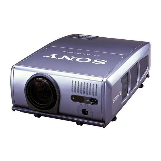
Sony VPD-LE100 Service Manual
Hide thumbs
Also See for VPD-LE100:
- Specifications (7 pages) ,
- Operating instructions manual (44 pages)
Table of Contents
Advertisement
Quick Links
Sony Corporation
Communication System Solutions Network Company
9-929-677-01
English
00DS16111-1
Printed in Japan
©2000.4
SERVICE MANUAL
MODEL
DEST.
CHASSIS NO.
..............
.........
....................
VPD-LE100
World
IFB-LE100
World
VPD-LE100
DATA PROJECTOR
IFB-LE100
INTERFACE BOARD
VPDL-Z1014/Z1019/
PROJECTION LENS
Z1023/Z1037
MODEL
DEST.
CHASSIS NO.
..............
.........
....................
VPDL-Z1014
World
VPDL-Z1019
World
VPDL-Z1023
World
VPDL-Z1037
World
DATA PROJECTOR
Advertisement
Chapters
Table of Contents
Troubleshooting

Related Manuals for Sony VPD-LE100


Summary of Contents for Sony VPD-LE100
- Page 1 SERVICE MANUAL MODEL MODEL DEST. CHASSIS NO. DEST. CHASSIS NO..................VPD-LE100 VPDL-Z1014 World World IFB-LE100 VPDL-Z1019 World World VPDL-Z1023 World VPDL-Z1037 World VPD-LE100 DATA PROJECTOR IFB-LE100 INTERFACE BOARD VPDL-Z1014/Z1019/ PROJECTION LENS Z1023/Z1037 English DATA PROJECTOR...
- Page 2 DIAGRAMS, EXPLODED VIEWS AND IN THE PARTS LIST ARE LES SCHÉMAS DE PRINCIPE, LES VUES EXPLOSÉES ET LES CRITICAL TO SAFE OPERATION. REPLACE THESE COMPO- NENTS WITH SONY PARTS WHOSE PART NUMBERS APPEAR LISTES DE PIECES SONT D’UNE IMPORTANCE CRITIQUE POUR LA SÉCURITÉ DU FONCTIONNEMENT. NE LES AS SHOWN IN THIS MANUAL OR IN SUPPLEMENTS PUB- LISHED BY SONY.
- Page 3 Table of Contents 1. Operating Instructions 1-1. VPD-LE100 Operating Instructions ............1-1 1-2. VPD-LE100 Installation Manual for Dealers ........... 1-23 1-3. VPD-LE100 Projection Distance Charts ........... 1-49 1-4. IFB-LE100 Operating Instructions ............1-61 1-5. VPDL-Z1014/Z1019/Z1023/Z1037 Operating Instructions ..... 1-62 1-6.
- Page 4 3-3. Optical Unit Block Assembly Adjustment ..........3-4 3-3-1. Integrator Adjustment ..............3-4 3-3-2. Reflective Mirror Adjustment ............ 3-6 3-4. Registration Adjustment ................3-6 3-4-1. GREEN Adjustment ..............3-6 3-4-2. BLUE Adjustment ..............3-8 3-5. Top/Bottom/Right/Left Focus Adjustment ..........3-8 3-5-1.
- Page 5 8. Block Diagrams Overall (1/2) ....................8-1 Overall (2/2) ....................8-2 ....................8-3 BA (1/2) ....................8-4 BA (2/2) ....................8-5 BB (1/2) ....................8-6 BB (2/2) ....................8-7 BC, P ....................8-8 QC (1/3), NA, NB (1/2) ................8-9 M (1/3), QC (2/3) ..................
- Page 6 BB (10/18) ....................9-39 BB (11/18) ....................9-40 BB (12/18) ....................9-41 BB (13/18) ....................9-42 BB (14/18) ....................9-43 BB (15/18) ....................9-44 BB (16/18) ....................9-45 BB (17/18) ....................9-46 BB (18/18) ....................9-47 BC (1/2) ....................9-50 BC (2/2) ....................
- Page 7 ROM in dotazione. Se occorre una copia dei manuali non in lingua inglese, è possibile visualizzare i manuali del CD-ROM a video oppure stamparli. • Se si utilizza il CD-ROM, leggere la sezione “ReadMe” che spiega come utilizzare il CD-ROM. VPD-LE100 © 2000 Sony Corporation...
- Page 8 For the customers in the United Kingdom WARNING AVERTISSEMENT WARNING THIS APPARATUS MUST BE EARTHED To prevent fire or shock hazard, do not Afin d’éviter tout risque d’incendie et d’électrocution, ne Pour les utilisateurs au Canada expose the unit to rain or moisture. IMPORTANT Cet appareil numérique de la classe A est conforme à...
-
Page 9: Table Of Contents
Table of Contents Overview Precautions ................6 Features .................. 7 Location and Function of Controls ........8 Front .................... 8 Control Panel ................10 Rear ................... 12 Remote Commander ..............14 Setting up and projecting Precautions on Installation ..........17 Installing the Projector ............ -
Page 10: Precautions
The combination of a 2 kW arc Xenon lamp and Digital greatly expanded. The projector also has the group and unplug the unit and have it checked by qualified Sony should not be exposed to direct lighting or sunlight. Light Processing... -
Page 11: Location And Function Of Controls
Using the carrying handles When attaching the optional lens, consult with Use the front and rear carrying handles to carry the q; Left side ventilation holes (exhaust) qualified Sony personnel. projector. To raise To lower qa Left side ventilation holes (intake) 3 Carrying handle Pull up. -
Page 12: Control Panel
Location and Function of Controls Location and Function of Controls Control Panel 8 LENS CONTROL keys qs SWITCHER keys FOCUS: Enters the focus adjustment mode. Adjust When the PC-3000 switcher is connected to the the focus using the arrow keys. projector, press a number key (1 to 8) to select the M: Focuses on a forward picture. -
Page 13: Rear
Location and Function of Controls Rear qa CONTROL S IN/OUT jacks (stereo minijack) qf REMOTE connectors Connect to the control S jacks of other Sony Used to expand system capability. equipment. RS-232C/RS-422A select switch: Selects according CONTROL S IN/PLUG IN POWER (DC 5 V... -
Page 14: Remote Commander
Location and Function of Controls Location and Function of Controls Remote Commander qg SWITCHER/VIDEO MEMORY/INDEX select 7 Transmission indicator switch The light goes on each time a key is pressed. If the Selects the function of the SWITCHER/VIDEO The Remote Commander can be used as a wireless or indicator does not light, replace the batteries. -
Page 15: Precautions On Installation
Precautions on Installation Location and Function of Controls Notes on batteries wa POSITION +/– keys Avoid installing the projector in a location Precautions on Installation • Make sure that the battery orientation is correct when These keys do not function with this projector. subject to excessive dust inserting batteries. -
Page 16: Installing The Projector
“Projection Distance Charts.” installing the projector on the floor. SET SETTING INPUT-A STATUS: You can select one of seven languages for the menus For ceiling installation, consult with qualified Sony LANGUAGE: ENGLISH and other on-screen displays. The factory setting is INSTALLATION: FRANCAIS personnel. -
Page 17: Projecting
M or m the optional IFB-LE100 interface board which key, the adjustment inside the projector may be is installed in the INPUT D section. required. Please consult with qualified Sony personnel. -
Page 18: Using The Menu
Using the Menu The PICTURE CTRL Menu To clear the menu display D. (dynamic) PICTURE Using the Menu The PICTURE CTRL Emphasizes the black color. Press the MENU key. The menu display also Menu The projector is equipped with an on-screen menu for OFF: Reproduces the dark portions of the picture disappears automatically if no key is pressed for one making various adjustments and settings. -
Page 19: The Input Setting Menu
The INPUT SETTING Menu The PICTURE CTRL Menu/The INPUT SETTING Menu SCAN CONV (converter) COMPONENT FORMAT Input signals and adjustable/setting items The INPUT SETTING Menu Converts the signal to display the picture so that it fits Selects the input component signal. Input signal SMPTE/EBU-N10: Set to this position if the input the screen size. -
Page 20: The Set Setting Menu
The INPUT SETTING Menu The INPUT SETTING Menu/The SET SETTING Menu About the memory function Memory Horizontal Memory Horizontal Preset signal Sync Preset signal Sync The SET SETTING Menu The adjustment data for 49 types of input signals are (kHz) (Hz) size (kHz) (Hz) size... -
Page 21: The Signal Select Menu
The SET SETTING Menu/The SIGNAL SELECT Menu The SIGNAL SELECT Menu POWER SAVING INPUT-C The SIGNAL SELECT Menu OFF: The power saving function does not operate. Selects the input signal from the connectors on the ON: The projector goes into the power saving mode optional IFB-12A interface board installed in the and the lamp for light source turns off if no signal INPUT C section. -
Page 22: Connection Examples
Connection Examples Connection Examples Connecting the Switcher Connection Examples Use the optional PC-3000 Signal Interface Switcher • When connecting the switcher, use the wired Remote When making connections, be sure to: Connecting a BNC connector for connecting various video equipment. The input can Commander. -
Page 23: Confirming The System Construction
Setting the Index Numbers Connection Examples Connection Examples Confirming the System When a system error is detected Notes on setting of the index number Setting the Index Construction • Set the same group index number for all The following messages are displayed on the screen Numbers equipment of the same system connection (those After all the connections are complete, confirm that... -
Page 24: Lamp Life
Remote Commander. When GROUP t 2 t ENTER t 1 t ENTER index numbers this message appears, consult with qualified Sony Projector C is selected. personnel for the lamp replacement. When the switchers and projectors are connected as... -
Page 25: Troubleshooting
28) . The power has been turned off using Wait for about one minute before turning on Consult with qualified Sony personnel for the The lamp is near the end of its life. the power (page 10) . lamp replacement. - Page 26 If the temperature does not lower after about one hour, the lamp filters may be clogged. Have the filters cleaned regularly by qualified Sony personnel. Consult with qualified Sony personnel for the lamp Replace the lamp. Replace the Lamp replacement.
-
Page 27: Specifications
Power off: 0 V VPS-100FH (100-inch, flat) VPS-120FH (120-inch, flat) Some of the items may not be available in some areas. For details, please consult your nearest Sony office..........................................1) ANSI lumen is a measuring method of American National Standard IT 7.228. -
Page 28: Index
Specifications Index Pin assignment Acceptable HDTV/DTV formats Index Handle release button 9 Remote Commander RS-232C/422A connector (D-sub 9-pin, female) H FILTER 25 battery installation 16 Format Scanning Frame Scanning Aspect Standard HUE 23 connecting to the projector 16 rate (kHz) rate (Hz)* format ratio... - Page 29 ROM in dotazione. Se occorre una copia dei manuali non in lingua inglese, è possibile visualizzare i manuali del CD-ROM a video oppure stamparli. • Se si utilizza il CD-ROM, leggere la sezione “ReadMe” che spiega come utilizzare il CD-ROM. VPD-LE100 © 2000 Sony Corporation Sony Corporation Printed in Japan...
- Page 30 This Installation Manual for Dealers explains how to install the projector. Table of Contents For example, it explains how to attach the lens and connect external equipment. Precautions ................4 For installation examples with projection distances, refer to the supplied “Projection Distance Charts.”...
-
Page 31: Precautions
Be aware that room heat rises to the damage the cabinet. unplug the unit and have it checked by qualified Sony ceiling; check that the temperature near the • Avoid touching the lens. To remove dust on the lens, personnel before operating it further. -
Page 32: Location And Function Of Controls
When attaching the optional lens, consult with Use the front and rear carrying handles to carry the To lower q; Left side ventilation holes (exhaust) To raise qualified Sony personnel. projector. qa Left side ventilation holes (intake) Pull up. 3 Carrying handle Pull out the handle for carrying the projector. -
Page 33: Control Panel
Location and Function of Controls Location and Function of Controls Control Panel 8 LENS CONTROL keys qs SWITCHER keys FOCUS: Enters the focus adjustment mode. Adjust When the PC-3000 switcher is connected to the the focus using the arrow keys. projector, press a number key (1 to 8) to select the M: Focuses on a forward picture. -
Page 34: Rear
Location and Function of Controls qa CONTROL S IN/OUT jacks (stereo minijack) qf REMOTE connectors Rear Connect to the control S jacks of other Sony Used to expand system capability. equipment. RS-232C/RS-422A select switch: Selects according CONTROL S IN/PLUG IN POWER (DC 5 V... -
Page 35: Remote Commander
Location and Function of Controls Location and Function of Controls Remote Commander 6 STATUS ON/OFF keys Note Note Press OFF to eliminate the on-screen display. After connecting the PC-3000 switcher and pressing The service adjustment keys qk to wf can function Press ON to restore the on-screen display. - Page 36 Location and Function of Controls Location and Function of Controls ql ADJ R/G/B keys Notes on wireless Remote Commander ed CONTROL S OUT jack To connect the Remote Commander to the operation Select the color to be adjusted when adjusting the Connect the supplied remote commander cable to this projector •...
-
Page 37: Precautions On Installation
Precautions on Installation Tips on the Screen Front projection screen for ceiling installation Avoid installing the projector in a location Tips on the Screen Precautions on Installation The silver screen is recommended. You can get a subject to excessive dust picture that is two to four times brighter than that of For installation examples with projection distances, see the the white screen. -
Page 38: Attaching The Lens
Attaching the Lens Attaching the Lens Replace the lens ring performing step 3 in the Upper lens ring Attaching the Lens For the VPDL-Z1014 lens only Lens hole cover reverse order, and tighten the screws. Before attaching the lens to the projector, attach the lens shield (supplied with the lens) to the lens. - Page 39 Connection Examples Connection Examples Connecting the Switcher Connection Examples Use the optional PC-3000 Signal Interface Switcher • When connecting the switcher, use the wired Remote When making connections, be sure to: Connecting a BNC connector for connecting various video equipment. The input can Commander.
- Page 40 Connection Examples Connection Examples Connecting Multiple Projectors To connect two switchers • Set the SW NO switch on the switcher to be Notes Following are examples of multiple projectors. connected to the projector to 1. Install the IFB-12A • Set the device index number of the projector to be interface board onto the switcher, and set the IN/OUT connected to the switcher to 01.
-
Page 41: Connection Examples
Connection Examples Connection Examples Confirming the System When using the switcher When a system error is detected Construction When connecting two PC-3000 switchers, up to 15 Notes The following messages are displayed on the screen inputs can be selected as the input from the switchers. •... -
Page 42: Setting The Index Numbers
Connection Examples Setting the Index Numbers Setting the Index Numbers Connection Examples Example: Notes on setting of the index number Notes on connections when two or more Setting the Index To select all the projectors in all the groups switchers are used •... -
Page 43: Adjusting The Picture
Press the MENU key. The menu display also The menu display appears. required. Please consult with qualified Sony “FOCUS” appears on the screen during disappears automatically if no key is pressed for one The menu presently selected is highlighted in personnel. -
Page 44: Using The Menu
Using the Menu The PICTURE CTRL Menu ON: Emphasizes the black color to produce a bolder To clear the menu display Using the Menu The PICTURE CTRL “dynamic” picture. Press the MENU key. The menu display also Menu The projector is equipped with an on-screen menu for disappears automatically if no key is pressed for one making various adjustments and settings. -
Page 45: The Input Setting Menu
The INPUT SETTING Menu The PICTURE CTRL Menu/The INPUT SETTING Menu SCAN CONV (converter) COMPONENT FORMAT Input signals and adjustable/setting items The INPUT SETTING Menu Converts the signal to display the picture so that it fits Selects the input component signal. Input signal SMPTE/EBU-N10: Set to this position if the input the screen size. -
Page 46: The Set Setting Menu
The INPUT SETTING Menu The INPUT SETTING Menu/The SET SETTING Menu About the memory function Memory Horizontal Memory Horizontal Preset signal Sync Preset signal Sync The SET SETTING Menu The adjustment data for 49 types of input signals are (kHz) (Hz) size (kHz) (Hz) size... -
Page 47: The Signal Select Menu
The SET SETTING Menu/The SIGNAL SELECT Menu The SIGNAL SELECT Menu/Using the SERVICE MODE POWER SAVING INPUT-C Using the SERVICE The SIGNAL SELECT OFF: The power saving function does not operate. Selects the input signal from the connectors on the MODE Menu ON: The projector goes into the power saving mode... -
Page 48: Restoring The User Mode
Using the SERVICE MODE The SERVICE MODE Menus Restoring the USER MODE Press the M or m key to select the menu, then press OPERATION TIMER The SERVICE MODE the , key or the ENTER key. Indicates the total number of hours for which the The selected menu appears. -
Page 49: The W/B Adjust Menu
Never open the lamp cover yourself; consult Use the M or m key to select PRESET 1, PRESET with qualified Sony personnel. 2 or PRESET 3, then press the , or ENTER key. The projector enters into GAIN/BIAS adjustment Replacing Procedure mode. -
Page 50: Cleaning The Lamp Filters And Air Filter
Cleaning the Lamp Filters and Air Filter Cleaning the Lamp Filters and Air Filter Cleaning the Air Filter Remove the dust from the air filter with a vacuum Cleaning the Lamp cleaner or wash it. Air filter Press the STANDBY key to turn off the power of Filters and Air Filter the projector, then turn off the main power using the POWER switch. -
Page 51: Troubleshooting
Color balance is not correct. Picture has not been adjusted properly. Adjust the picture (page 30) . with qualified Sony personnel. The color system of the input signal is Set COLOR SYS in the PICTURE CTRL menu not set correctly. - Page 52 Clean the filters (page 42) . If the projector does not operate properly even after the lamp filter cleaning, consult with qualified Sony personnel. Replace the lamp (page 41) .
-
Page 53: Specifications
Power off: 0 V VPS-100FH (100-inch, flat) VPS-120FH (120-inch, flat) Some of the items may not be available in some areas. For details, please consult your nearest Sony office..........................................1) ANSI lumen is a measuring method of American National Standard IT 7.228. -
Page 54: Index
Specifications Index Pin assignment Acceptable HDTV/DTV formats Index Handle release button 7 Remote Commander RS-232C/422A connector (D-sub 9-pin, female) H FILTER 33 battery installation 14 Format Scanning Frame Scanning Aspect Standard HUE 31 connecting to the projector 15 rate (kHz) rate (Hz)* format ratio... - Page 55 4-075-698-01(1) Data Projector Projection Distance Charts pages 2–23 VPD-LE100 © 2000 Sony Corporation Sony Corporation Printed in Japan...
- Page 56 Tableau des ñ⁄éü Contents matières English Lens Types Used with the Projector ......... 2 How to Display the Picture ....4 Before Installation ......6 Installation Example ......8 5 : 4 ..........10 4 : 3 ..........14 Dimensions ........18 ......................
- Page 57 How to Display the Picture Screen Screen Screen Screen Sales Sales Sales Sales West 35% West 35% West 35% West 35% East 65% East 65% East 65% East 65% indicates the displayed picture. English Installation measurements vary depending on how you want to display the picture on the screen.
- Page 58 Before Installation Center of the lens Top view Screen 94.4 (3 Center of the screen Center of the projector Unit: mm (inches) English Checking the horizontal position of the picture C Install the projector so that the center of the lens is aligned with the horizontal center of the screen.
- Page 59 Installation Example Distance between the front of the cabinet and the center of the lens Center of the screen Wall VPDL-Z1014: 36.9 (1 VPDL-Z1019: 40.4 (1 VPDL-Z1023: -23.7 (- VPDL-Z1037: 87.9 (3 Center of the lens Unit: mm (inches) Floor English This section describes an example for installing the projector on the desk, etc.
- Page 60 Unit: mm (inches) Unit: mm (inches) p VPDL-Z1014 p VPDL-Z1019 2670 3840 4620 5790 6960 7740 9680 11630 1950 2830 3420 4300 5170 5760 7220 8690 (111 (134 (169) (203 (226 (284 (342) (104 (150 (181 (227 (273 (304 (381 (457 2590 3770...
- Page 61 Unit: mm (inches) Unit: mm (inches) p VPDL-Z1023 p VPDL-Z1037 5140 7430 8950 11240 13520 15050 18860 22670 3180 4610 5560 6990 8420 9380 11760 14150 (125 (181 (219) (275 (331 (369 (463) (556 (202 (292 (352 (442 (532 (592 (742 (892 9040...
- Page 62 Unit: mm (inches) Unit: mm (inches) p VPDL-Z1014 p VPDL-Z1019 2850 4100 4930 6180 7420 8250 10330 12410 2090 3030 3650 4590 5530 6150 7710 9270 (119) (143 (180 (217 (242) (303 (365 (112) (161 (193 (243) (292 (324 (406 (488 2780 4030...
- Page 63 Unit: mm (inches) Unit: mm (inches) p VPDL-Z1023 p VPDL-Z1037 5500 7940 9560 12000 14440 16070 20130 24200 3400 4930 5950 7470 9000 10010 12560 15100 (133 (193 (234) (294) (354 (394 (494 (594 (216 (312 (376 (472 (568 (632 (792 (952 9660...
- Page 64 Dimensions Abmessungen English Necessary Clearance for Installation and Maintenance Make sure to provide enough room for maintenance service. Install the projector, making reference to the dimensions shown on pages 18 to 21. Also, there should be an enough space around the exhaust and intake holes without blocking them.
- Page 65 Dimensions Top (excluding the lens) Bottom (excluding the lens) 651.0 (25 724.0 (28 300.0 (11 94.4 (3 21.0 ( 420.0 (16 Unit: mm (inches) 582.0 (23) a: Center of the lens b: Ventilation hole (intake) d: Center of the projector f: Center of projection balance g: Mounting screw hole (4 - M12) Dimensions from the front of...
- Page 66 Dimensions English Scattering area if lamp breaks Should the lamp break, broken pieces may be scattered around the projector. To avoid risk of injury, place a tray to receive pieces or keep a no-go area around the projector, making reference to the figures below.
- Page 67 HD SDI English How to Use The IFB-LE100 interface board is a PC board to be mounted on Sony VPD-LE100 Data Projector to input the HDTV serial digital signal and 1 Select INPUT SELECT “D” with the Remote Commander supplied with the projector or the control panel of the projector.
- Page 68 English The VPDL-Z1014/Z1019/Z1023/Z1037 projection lenses are zoom lenses designed for use with the Sony VPD-LE100 Data Projector. About Lens Attachment Attaching the lens may cause fire or injury to the person. Users should request qualified Sony representative to attach the lens.
- Page 69 Projector Lamp The LMP-L2000 lamp is designed to be used exclusively with the Sony VPD-LE100 Data Projector. Do not use it for any other projector as doing so may lead to breakdown or fire. To replace the lamp, contact your authorized Sony dealer.
- Page 71 Section 2 Service Informations 2-1. Circuit Boards Location LINE DOUBLER FORMATTER POWER SUPPLY BLOCK VPD-LE100A/LE100E/LE100U...
- Page 72 2-2. Disassembly 2-2-1. Panel Removal 1 Two fasteners 3 Top panel (RE) Rotate here by 90° and remove the fasteners 7 Four screws (+PSW4 x 12) 2 Top panel CN701 (FR) !- Fifteen screws 8 Side panel XA board (+PSW4 x 12) (L) assy != Inner shield (Top) assy...
- Page 73 2-2-2. UA Board Removal 1 Two fasteners Rotate here by 90° and remove the fasteners CN911 4 UA board 3 Two screws (+PWH3 x 8) 2 Lamp cover assy 2-2-3. Lens Removal 1 Loosen the screw 2 Lens VPD-LE100A/LE100E/LE100U...
- Page 74 2-2-4. M, BA (Line Doubler Board) and BB Boards Removal and Check 1 Two screws (+PSW4 x 12) 2 BLK shield (Top) 4 BA board XBA Extension board A-1391-047-A Line doubler board 5 BB board 3 M board VPD-LE100A/LE100E/LE100U...
- Page 75 2-2-5. Formatter Board Removal ..Remove the top frame (CTR) assy. (Refer to 2-2-6.) ..Remove the duct (F). (Refer to 2-2-7.) 1 Two screws (+PSW4 x 12) 2 BLK cover Two hooks 3 Formatter board Three connectors VPD-LE100A/LE100E/LE100U...
- Page 76 2-2-6. BC Board Removal and Check Remove the connectors 1 Six screws 3 BC board CN505 (+BV4 x 12) CN902 CN504 CN506 CN507 CN502 CN503 CN501 2 Top frame (CTR) assy XE Extension board A-1501-122-A VPD-LE100A/LE100E/LE100U...
- Page 77 2-2-7. Prism Block Removal ..Remove the formatter board. (Refer to 2-2-5.) ..Remove the BC board. (Refer to 2-2-6.) !- Three screws (+PS3 x 20) 5 Screw (+PSW4 x 12) 6 R plate guide != Prism block 3 Duct (B) 9 Four screws...
- Page 78 2-2-8. XB Board Removal 4 XB board 2 XB cover assy 3 Two screws (+PSW4 x 12) 1 Eight screws (+BV4 x 12) 2-2-9. QA, QC and NB Boards Removal and Check !- Two screws (+PS3 x 8) CN901 7 Four screws != NB board (+B3 x 12) 0 Bracket (LCD)
- Page 79 2-2-10. XA Board Removal ..Remove the XB board. (Refer to 2-2-8.) ..Remove the QA, QC and NB boards. (Refer to 2-2-9.) 1 Five screws (+BV4 x 12) CN701 CN703 CN704 3 Five screws (+PSW4 x 12) CN702 CN705...
- Page 80 2-2-11. Power Supply Block Removal 2 Two bolts 1 Three screws (+PSW4 x 12) CN22 CN23 3 Power supply block IGN. AC INPUT 2-10 VPD-LE100A/LE100E/LE100U...
- Page 81 2-2-12. G and F Boards Removal and Check ..Remove the BC board. (Refer to 2-2-6.) ..Remove the power supply block. (Refer to 2-2-11.) 1 Two screws (+PSW4 x 12) 2 G cover assy 3 G board CN601 CN650...
- Page 82 2-2-13. BM Board Removal ..Remove the lens. (Refer to 2-2-3.) ..Remove the M, BA and BB boards. (Refer to 2-2-4.) ..Remove the formatter board. (Refer to 2-2-5.) .
- Page 83 2-2-14. Preparation for “When Prism is Replaced” 1 Remove the commander holder block assy. (Refer to 2-2-1.) 3 Attach the commander holder block assy with the connector kept connected. 2 Slide the top frame (CTR) assy to an appropriate position that enable the prism adjustment.
- Page 84 2-3. Note Note 1 When a lamp is broken, there can be case that the lamp debris is splashed out of the lamp house and is left inside the equipment. Therefore, put on the gloves not to damage hands with be debris before starting the lamp replacement.
- Page 85 1. Attach an extension board to the BA board. 3. Oscilloscope (Part No : A-1391-047-A XBA extension board) Sony Textronix 2465 or equivalent (350 MHz band 2. Connect CH1 of the oscilloscope to the TP963/BA width or more) board and CH2 to the TP1301/BA board (EXT TRIG).
- Page 86 3-1-2. VIDEO NTSC Level Adjustment 3-1-4. Y, Pb and Pr Level Adjustment 1. Connect the NTSC composite 100% color bar signal to 1. Connect the HDVS (1080/60I) 100% color bar signal the INPUT-B connector and select VIDEO as SIG- to the INPUT-A connector and select YpbPr as NAL SELECT.
- Page 87 3-2. W/B Adjustment 3-2-2. W/B Adjustment (6500K) 3-2-1. W/B Adjustment (9300K) 1. Connect the SXGA 100% flat field 60 Hz signal to the INPUT-A signal and select COMPUTER as SIGNAL 1. Connect the SXGA 100% flat field 60 Hz signal to the SELECT.
- Page 88 3-3. Optical Unit Block Assembly 3-2-3. W/B Adjustment (5400K) Adjustment 1. Connect the SXGA 100% flat field 60 Hz signal to the 3-3-1. Integrator Adjustment INPUT-A connector and select COMPUTER as SIGNAL SELECT. 2. Set CONTRAST to 90. 1. Press the PATTERN key on the control panel, select 3.
- Page 89 14. After adjustment is complete, fix screws 1 and 2 12. Move screws A and B shown in Fig. 8 to decrease the area outside the lines searched in step 11 so that the shown in Fig. 7. integrator image is inside the square of bright lines. Bright line Integrator image 3 Integrator...
- Page 90 (+) in the following order so that the 45 °C. illumination reaches the maximum. 4. Adjust the X/Y direction adjustment screw with the 1.5-mm hexagon wrench. VPD-LE100 Convex lens Illuminance meter Y-direction adjustment Reflective mirror Adjustment hole position Fig. 9...
- Page 91 The relation between screw rotation and image movement is as follows. a) Movement when turning screw A clockwise (fasten the screw): b) Movement when turning screw A counterclockwise (loosen the screw): c) Movement when turning screw B clockwise (fasten the screw): d) Movement when turning screw B counterclockwise (loosen the screw): e) Movement when turning screw C clockwise (fasten...
- Page 92 3-5. Top/Bottom/Right/Left Focus 3-4-2. BLUE Adjustment Adjustment 1. Perform the BLUE adjustment in the same way as Preparation GREEN adjustment while referring to Fig. 12. 1. Enter the service mode. Y-direction adjustment 2. Press the PATTERN key on the control panel and select the crosshatch signal.
- Page 93 3-6. QC Board Adjustment 3-5-1. Top/Bottom Focus Adjustment 3-6-1. Current Detection 0 Set Adjustment 1. Loosen the locking screws for the top/bottom focus adjustment screw on the lens shift block. 2. Adjust the focus in the center of the screen with the Remove all the signals (open) from the CONTROL-S IN remote control.
- Page 95 Section 4 Trouble Shooting 4-1. Display of LED Panel Check the display of the LED panel next to the input panel of the main unit. . Around T102 fails on G board . Around T103 fails on G board . Around T104 fails on G board →...
- Page 96 . Lamp does not strike → The lamp does not light. When the system detects that no current is supplied from the lamp power supply, this message is displayed. This happens when the lamp reaches the end of its lifespan. Replace the lamp with a new one before this happens.
- Page 97 4-2. Power Supply The standby state is not entered even when the power supply switch is turned on. (The standby LED on the control panel does not light.) START F101 open? The SUB+5 V line and the GND line could be shorted on the load side. Check them with the tester.
- Page 98 Standby power is output, but analog circuit power (24 V, 13.5 V, 6.2 V, _6.2 V) is not output even when the power is turned on (in case PROT T102 is displayed). START Pin No. A6 of CN602 is not set to H (5 V). Power ON signal is not output from the microprocessor side.
- Page 99 Standby power is output, but analog circuit power (3.3 V, 5.0 V, _5.2 V, _2 V) is not output even when the power is turned on (in case PROT T103 is displayed). START Pin No. A6 of CN602 is not set to H (5 V). Power ON signal is not output from the microprocessor side.
- Page 100 Standby power is output, but Peltier and fan circuit power (9 V, 12 V) are not output even when the power is turned on (in case PROT T104 is displayed). START Pin No. A6 of CN602 is not set to H (5 V). Power ON signal is not output from the microprocessor side.
- Page 101 Section 5 Semiconductors 74LCX08MTCX BA033FP-E2 CXA1855Q CXD2315Q 74LCX32MTCX BA05FP-E2 74LCX74MTCX BA09FP-E2 MAX489ECSD-TE2 BA12FP-E2 NJM2901M-TE2 PC74HC08D-T TOP VIEW PC74HC14D-T 32pin QFP TC74HC04AF(EL) TC74HC32AF(EL) TOP VIEW CXD8675R TC74HCT08AF(EL) CXD8773R TC74HCU04AF(EL) HD6437043AE65F CXA2101AQ-TL TC74VHC02F(EL) IP90C63A CXD2024AQ TC74VHC08F(EL) CXD8774R TC74VHC32F(EL) CXP84648-071Q TC74VHCT04AF(EL) TLC2932IPW-E20 CXA1166K TLC2933IPWR CY7C136-55JC TOP VIEW...
- Page 102 IC, Transistor ISPLSI1016E-125LT44-BB03V1 MBCG46104-120PFV M48Z35Y-70PC1 TC4S71F(TE85R) ISPLSI1016E-80LT44-BB02V3 TC7S04FU(TE85R) ISPLSI1016E-80LT44-BB05V1 TC7S86FU(TE85R) ISPLSI1016E-80LT44-M02V1 TC7SET08FU(TE85R) ISPLSI2032-80LT48-M01V1 TC7SH04F(TE85R) TC7SH08F-TE85R TOP VIEW TC7SH32F-TE85L 240pin QFP TC7SH32FU-TE85R TLV431ACDBV2 MBM29F400BC-70PFTN PC16552DV TOP VIEW INDEX 44pin QFP LM2990SX-5.0 5pin CHIP TOP VIEW TOP VIEW TC551664BJ-15(EL) MBM29LV002T-ORION 44pin QFJ INDEX PC74HC32D-T TOP VIEW...
- Page 103 Transistor, Diode 2SA1037K-T-146-QR 2SD2144S-TP-V 1SS123-T1 D10SC4MR 2SA1162-YG-TE85L DA204K-T-146 2SA1182-Y(TE85R) DA204UT106 2SA1462-T1Y33Y34 DCC010-TB 2SA1462-T1Y34 MA157-TX 2SB1440S-TX 2SC2412K-T-146-QR 2SC2712-YG-TE85L 2SC3326N-TE85L-B 2SC3545-T1T43T44 2SC3624A-T1L15 DTC114EKA-T146 DTC143ZUA-T106 2SK2281-4061 DTC144EKA-T146 D10SC9M 1SS355TE-17 MA111-TX RD12SB2-T1 RD13SB2-T1 2SA1358-Y 2SK3013F-02 UDZ-TE-17-3.9B ANODE CATHODE D6SB80 1S2836-T1 FMS1-T-148 2SB772-Q 2SD882-P LETTER SIDE FCH20A10 1S2837-T1 FCQ20A04...
- Page 104 Diode GP08DPKG23 RD5.6SB2-T1 P6KE200AG23 RGP10G RGP10JPKG23 ZP2600 EL1Z CATHODE SEC1401C SEC1801C ANODE CATHODE MARK MVR3368S TF861S CATHODE ANODE P6KE300A P6KE350AG23 CATHODE ANODE GATE TLG113A RD20M-T1B2 ANODE RD24M-T1B1 CATHODE RD5.1M-T1B2 RD8.2M-T1B2 TLR113A CATHODE ANODE RD39ES-T1B2 TLR124 CATHODE ANODE ANODE CATHODE VPD-LE100A/LE100E/LE100U...
- Page 105 Section 6 Exploded Views NOTE : • Items marked “ * ” are not stocked since they are seldom required The components identified marked ! are for routine service. Some delay should be anticipated when order- critical for safety. ing these items. Replace only with the part number specified.
- Page 106 Panel 6-1. Panel : 7-621-283-00 +P2x5 : 7-682-663-09 +PSW4x12 : 7-682-903-21 +PWH3x8 : 7-685-661-79 +BV4x12 Ref.No. Part No. Description Remark Ref.No. Part No. Description Remark * X-4037-676-1 RING (A) ASSY, LENS 2, 3 * 4-075-910-01 LID, LENS ADJUSTMENT 4-076-037-01 SCREW (A), SPECIAL * 4-075-929-01 COVER, FILTER 4-076-043-01 WASHER, LENS RING * X-4037-679-1 SHIELD (TOP) ASSY, INNER...
- Page 107 Chassis 6-2. Chassis : 7-682-663-09 +PSW4x12 : 7-682-648-09 +PS3x8 : 7-682-246-09 +K3x5 : 7-682-653-09 +PS3x20 : 7-682-965-01 +PSW4x16 : 7-685-661-79 +BV4x12 Ref.No. Part No. Description Remark Ref.No. Part No. Description Remark * 1-676-177-11 PWB, NA * A-1136-063-A BC COMPL ! 1-794-330-11 INLET, AC * 4-075-881-01 GUIDE, R PLATE * 4-076-040-01 PLATE (C), REMOCON * 4-075-901-01 BRACKET, BREAKER...
- Page 108 Rear Case 6-3. Rear Case : 7-682-663-09 +PSW4x12 : 7-682-544-04 +P3x3 : 7-685-246-19 +KTP3x8 : 7-682-903-11 +PWH3x6 : 7-628-000-05 +PSW2x6 : 7-685-661-79 +BV4x12 : 7-621-256-25 M2x20 : 7-682-961-09 +PSW4x8 : 7-682-652-09 +PS3x16 : 7-682-648-09 +PS3x8 : 7-623-205-22 SW2 : 7-688-001-01 W2 LMP-L2000 PROJECTOR LAMP Ref.No.
- Page 109 G Shield Block 6-4. G Shield Block : 7-621-283-00 +P2x5 : 7-682-663-09 +PSW4x12 : 7-682-969-09 +PSW4x35 : 7-685-661-79 +BV4x12 : 7-682-903-21 +PWH3x8 Ref.No. Part No. Description Remark Ref.No. Part No. Description Remark 1-763-417-11 FAN, DC * 4-056-414-01 BUSHING, SQUARE 1-239-366-11 FILTER, NOISE (MXB-1220-33) 3-701-822-01 HOLDER, WIRE ! 1-468-509-11 SUPPLY BLOCK, POWER * 4-075-912-01 COVER (FR-R), FILTER...
- Page 110 Base Assy 6-5. Base Assy : 7-682-260-09 +K4x6 : 7-682-263-09 +K4x12 : 7-685-661-79 +BV4x12 Ref.No. Part No. Description Remark Ref.No. Part No. Description Remark * 4-076-055-11 STOPPER, GRIP * 4-075-913-01 CLIP, SIDE * 4-075-970-01 HANDLE, T * 4-075-914-01 GRIP, CENTER * 4-076-055-01 STOPPER, GRIP * 4-075-969-01 PIPE (FR), HANDLE * 4-075-880-01 SUPPORT, BASE...
- Page 111 Prism Block 6-6. Prism Block : 7-682-648-09 +PS3x8 : 7-682-248-09 +K3x8 Ref.No. Part No. Description Remark Ref.No. Part No. Description Remark * 4-075-981-01 HEAT SINK (TIR) 1-251-875-11 ELEMENT, THERMO COOLER * 4-075-919-01 HOLDER, TIR * 4-075-944-01 HEAT SINK (TEC) 1-476-002-11 SENSOR, PHOTO * 4-075-976-01 HOLDER, HEAT SINK * 1-676-180-11 PWB, P * 4-076-221-01 HOLDER (TEC)
- Page 112 IFB-LE100 6-7. IFB-LE100 : 7-682-247-09 +K3x6 : 7-621-592-00 +K2.6x6 : 7-682-647-09 +PS3x6 Ref.No. Part No. Description Remark Ref.No. Part No. Description Remark 1-763-038-11 MOTOR, DC FAN 4-032-851-01 HANDLE 4-076-335-01 PANEL (HD), REAR * A-1131-585-A BF MOUNT 1-782-944-11 CABLE ASSY, COAXIAL 4-396-203-01 SCREW (+B M3X12) VPD-LE100A/LE100E/LE100U...
- Page 113 VPDL-Z1014/Z1019/Z1023/Z1037 6-8. VPDL-Z1014/Z1019/Z1023/Z1037 Ref.No. Part No. Description Remark Ref.No. Part No. Description Remark * 4-076-338-01 SHIELD, LENS (Z1014) 9-885-006-42 ZOOM MOTOR UNIT * X-4037-742-1 SHIELD ASSY, LENS (Z1019,Z1023,Z1037) 9-885-006-44 LENS CAP, REAR (Z1014) 4-076-664-01 MANUAL INSTRUCTION 9-885-006-46 LENS CAP, REAR (Z1019) (JAPANESE, ENGLISH, FRENCH, 9-885-006-39 LENS CAP, REAR (Z1023) 9-885-006-41 LENS CAP, REAR (Z1037)
- Page 115 Section 7 Electrical Parts List NOTE : • Items marked “ * ” are not stocked since they are seldom required The components identified marked ! are for routine service. Some delay should be anticipated when critical for safety. ordering these items. Replace only with the part number specified.
- Page 116 Ref.No. Part No. Description Remark Ref.No. Part No. Description Remark C177 1-163-239-11 CERAMIC CHIP 33PF C466 1-117-681-11 ELECT CHIP 100µF C180 1-128-004-11 ELECT CHIP 10µF C467 1-164-004-11 CERAMIC CHIP 0.1µF C181 1-128-004-11 ELECT CHIP 10µF C468 1-163-021-91 CERAMIC CHIP 0.01µF C191 1-128-004-11 ELECT CHIP 10µF...
- Page 117 Ref.No. Part No. Description Remark Ref.No. Part No. Description Remark C583 1-164-004-11 CERAMIC CHIP 0.1µF C787 1-164-004-11 CERAMIC CHIP 0.1µF C584 1-107-823-11 CERAMIC CHIP 0.47µF C791 1-126-204-11 ELECT CHIP 47µF C601 1-163-227-11 CERAMIC CHIP 10PF 0.50PF 50V C793 1-126-204-11 ELECT CHIP 47µF C602 1-163-021-91 CERAMIC CHIP 0.01µF...
- Page 118 Ref.No. Part No. Description Remark Ref.No. Part No. Description Remark C928 1-109-982-11 CERAMIC CHIP 1µF C1160 1-164-004-11 CERAMIC CHIP 0.1µF C929 1-126-204-11 ELECT CHIP 47µF C1161 1-164-004-11 CERAMIC CHIP 0.1µF C930 1-164-004-11 CERAMIC CHIP 0.1µF C1201 1-164-004-11 CERAMIC CHIP 0.1µF C931 1-107-823-11 CERAMIC CHIP 0.47µF C1202...
- Page 119 Ref.No. Part No. Description Remark Ref.No. Part No. Description Remark C1511 1-164-004-11 CERAMIC CHIP 0.1µF C9103 1-164-004-11 CERAMIC CHIP 0.1µF C1512 1-164-004-11 CERAMIC CHIP 0.1µF C9104 1-164-004-11 CERAMIC CHIP 0.1µF C1551 1-164-004-11 CERAMIC CHIP 0.1µF C9105 1-126-205-11 ELECT CHIP 47µF 6.3V C1552 1-128-004-11 ELECT CHIP...
- Page 120 Ref.No. Part No. Description Remark Ref.No. Part No. Description Remark C9420 1-164-004-11 CERAMIC CHIP 0.1µF <FERRITE BEAD> C9421 1-164-004-11 CERAMIC CHIP 0.1µF C9422 1-164-004-11 CERAMIC CHIP 0.1µF FB501 1-414-234-22 INDUCTOR CHIP0µH C9423 1-164-004-11 CERAMIC CHIP 0.1µF FB531 1-414-234-22 INDUCTOR CHIP0µH C9424 1-164-004-11 CERAMIC CHIP 0.1µF FB532...
- Page 121 Ref.No. Part No. Description Remark Ref.No. Part No. Description Remark IC704 8-759-038-15 IC MC74HC4538AFEL L451 1-414-754-11 INDUCTOR 10µH IC741 8-759-295-47 IC TDA9141-N2C L452 1-410-389-31 INDUCTOR CHIP47µH IC742 8-759-082-58 IC TC7W08FU(TE12R) L461 1-414-754-11 INDUCTOR 10µH IC771 8-759-565-20 IC TDA4665T/V5-118 L462 1-414-754-11 INDUCTOR 10µH IC772 8-759-335-57 IC MM1112XFBE...
- Page 122 Ref.No. Part No. Description Remark Ref.No. Part No. Description Remark <TRANSISTOR> Q791 8-729-230-49 TRANSISTOR 2SC2712-YG-TE85L Q792 8-729-230-49 TRANSISTOR 2SC2712-YG-TE85L Q101 8-729-107-31 TRANSISTOR 2SC3545-T1T43T44 Q793 8-729-230-49 TRANSISTOR 2SC2712-YG-TE85L Q131 8-729-107-31 TRANSISTOR 2SC3545-T1T43T44 Q794 8-729-230-49 TRANSISTOR 2SC2712-YG-TE85L Q161 8-729-107-31 TRANSISTOR 2SC3545-T1T43T44 Q795 8-729-230-49 TRANSISTOR 2SC2712-YG-TE85L Q321 8-729-216-22 TRANSISTOR 2SA1162-YG-TE85L...
- Page 123 Ref.No. Part No. Description Remark Ref.No. Part No. Description Remark R133 1-216-025-91 RES-CHIP 1/10W R361 1-216-049-91 RES-CHIP 1/10W R134 1-216-049-91 RES-CHIP 1/10W R362 1-216-031-00 RES-CHIP 1/10W R135 1-216-009-91 RES-CHIP 1/10W R363 1-216-651-11 METAL CHIP 0.50% 1/10W R136 1-216-623-11 METAL CHIP 0.50% 1/10W R364 1-216-659-11 METAL CHIP...
- Page 124 Ref.No. Part No. Description Remark Ref.No. Part No. Description Remark R502 1-216-645-11 METAL CHIP 0.50% 1/10W R701 1-216-017-91 RES-CHIP 1/10W R503 1-216-295-91 SHORT R702 1-216-053-00 RES-CHIP 1.5K 1/10W R504 1-216-025-91 RES-CHIP 1/10W R703 1-216-049-91 RES-CHIP 1/10W R505 1-216-647-11 METAL CHIP 0.50% 1/10W R704 1-216-065-91 RES-CHIP...
- Page 125 Ref.No. Part No. Description Remark Ref.No. Part No. Description Remark R804 1-216-057-00 RES-CHIP 2.2K 1/10W R924 1-216-017-91 RES-CHIP 1/10W R805 1-216-047-91 RES-CHIP 1/10W R925 1-216-017-91 RES-CHIP 1/10W R806 1-216-017-91 RES-CHIP 1/10W R926 1-216-017-91 RES-CHIP 1/10W R807 1-216-643-11 METAL CHIP 0.50% 1/10W R927 1-216-017-91 RES-CHIP 1/10W...
- Page 126 Ref.No. Part No. Description Remark Ref.No. Part No. Description Remark R1167 1-216-039-00 RES-CHIP 1/10W R1388 1-216-019-00 RES-CHIP 1/10W R1168 1-216-039-00 RES-CHIP 1/10W R1389 1-216-019-00 RES-CHIP 1/10W R1169 1-216-039-00 RES-CHIP 1/10W R1390 1-216-019-00 RES-CHIP 1/10W R1172 1-216-039-00 RES-CHIP 1/10W R1391 1-216-019-00 RES-CHIP 1/10W R1173 1-216-039-00 RES-CHIP...
- Page 127 Ref.No. Part No. Description Remark Ref.No. Part No. Description Remark R9060 1-216-621-11 METAL CHIP 0.50% 1/10W R9616 1-216-295-91 SHORT R9061 1-216-623-11 METAL CHIP 0.50% 1/10W R9620 1-216-295-91 SHORT R9062 1-216-624-11 METAL CHIP 0.50% 1/10W R9623 1-216-295-91 SHORT R9063 1-216-623-11 METAL CHIP 0.50% 1/10W R9624 1-216-295-91 SHORT...
- Page 128 BA BB Ref.No. Part No. Description Remark Ref.No. Part No. Description Remark RB1507 1-234-168-11 RES, CHIP NETWORK 27 (3216) C138 1-164-004-11 CERAMIC CHIP 0.1µF RB9601 1-236-908-11 RES, CHIP NETWORK 10K (3216) C139 1-164-004-11 CERAMIC CHIP 0.1µF RB9602 1-236-908-11 RES, CHIP NETWORK 10K (3216) C160 1-164-004-11 CERAMIC CHIP 0.1µF RB9603...
- Page 129 Ref.No. Part No. Description Remark Ref.No. Part No. Description Remark C410 1-164-004-11 CERAMIC CHIP 0.1µF C643 1-164-004-11 CERAMIC CHIP 0.1µF C411 1-164-004-11 CERAMIC CHIP 0.1µF C644 1-164-004-11 CERAMIC CHIP 0.1µF C412 1-164-004-11 CERAMIC CHIP 0.1µF C645 1-164-004-11 CERAMIC CHIP 0.1µF C413 1-164-004-11 CERAMIC CHIP 0.1µF C646...
- Page 130 Ref.No. Part No. Description Remark Ref.No. Part No. Description Remark C5217 1-164-004-11 CERAMIC CHIP 0.1µF IC52 8-759-490-41 IC TC74VHCT541AFT(EL) C5218 1-164-004-11 CERAMIC CHIP 0.1µF IC53 8-759-012-13 IC MC10H125MEL C5219 1-164-004-11 CERAMIC CHIP 0.1µF IC54 8-759-012-00 IC MC10H116MEL C5220 1-163-251-11 CERAMIC CHIP 100PF C5221 1-163-021-91 CERAMIC CHIP 0.01µF IC110...
- Page 131 Ref.No. Part No. Description Remark Ref.No. Part No. Description Remark <COIL> R420 1-216-295-91 SHORT R421 1-216-001-00 RES-CHIP 1/10W 1-409-529-41 INDUCTOR 10µH R422 1-216-009-91 RES-CHIP 1/10W 1-469-545-21 COIL, CHOKE (SMD) 10µH R423 1-216-295-91 SHORT 1-409-529-41 INDUCTOR 10µH R424 1-216-295-91 SHORT 1-469-545-21 COIL, CHOKE (SMD) 10µH R425 1-216-295-91 SHORT...
- Page 132 Ref.No. Part No. Description Remark Ref.No. Part No. Description Remark R495 1-216-009-91 RES-CHIP 1/10W R5208 1-216-295-91 SHORT R496 1-216-009-91 RES-CHIP 1/10W R5209 1-216-009-91 RES-CHIP 1/10W R601 1-216-049-91 RES-CHIP 1/10W R5210 1-216-009-91 RES-CHIP 1/10W R602 1-216-049-91 RES-CHIP 1/10W R5211 1-216-295-91 SHORT R603 1-216-049-91 RES-CHIP 1/10W...
- Page 133 BB BC Ref.No. Part No. Description Remark Ref.No. Part No. Description Remark RB132 1-233-575-11 RES, CHIP NETWORK 22 RB5209 1-233-575-11 RES, CHIP NETWORK 22 RB133 1-233-575-11 RES, CHIP NETWORK 22 RB5210 1-233-575-11 RES, CHIP NETWORK 22 RB134 1-233-575-11 RES, CHIP NETWORK 22 RB5211 1-233-575-11 RES, CHIP NETWORK 22 RB135...
- Page 134 Ref.No. Part No. Description Remark Ref.No. Part No. Description Remark 1-126-382-11 ELECT 100µF D300 8-719-045-53 DIODE SEC1801C 1-126-382-11 ELECT 100µF D301 8-719-105-82 DIODE RD5.1M-T1B2 1-164-004-11 CERAMIC CHIP 0.1µF D302 8-719-045-60 DIODE SEC1401C 1-164-004-11 CERAMIC CHIP 0.1µF D303 8-719-801-78 DIODE 1S2837-T1 1-126-786-11 ELECT 47µF D304...
- Page 135 BC BM Ref.No. Part No. Description Remark Ref.No. Part No. Description Remark 1-216-295-91 SHORT R115 1-216-675-91 METAL CHIP 0.50% 1/10W 1-216-083-00 RES-CHIP 1/10W R200 1-216-655-11 METAL CHIP 1.5K 0.50% 1/10W 1-216-025-91 RES-CHIP 1/10W R201 1-216-675-91 METAL CHIP 0.50% 1/10W 1-216-295-91 SHORT R202 1-216-049-91 RES-CHIP 1/10W...
- Page 136 BM F G Ref.No. Part No. Description Remark Ref.No. Part No. Description Remark <RESISTOR> C114 1-163-003-11 CERAMIC CHIP 330PF C115 1-107-889-11 ELECT 220µF 1-215-905-11 METAL OXIDE C116 1-165-319-11 CERAMIC CHIP 0.1µF C117 1-107-909-11 ELECT 47µF C118 1-164-492-11 CERAMIC CHIP 0.15µF *************************************************************** C119 1-163-113-00 CERAMIC CHIP 68PF...
- Page 137 Ref.No. Part No. Description Remark Ref.No. Part No. Description Remark C197 1-115-717-51 ELECT 0.0027F 20% 6.3V D135 8-719-510-13 DIODE D10SC4MR C198 1-115-767-51 ELECT 0.0027F 20% C199 1-115-717-51 ELECT 0.0027F 20% 6.3V D136 8-719-947-06 DIODE RGP10JPKG23 C200 1-115-339-11 CERAMIC CHIP 0.1µF D137 8-719-302-43 DIODE EL1Z C201...
- Page 138 Ref.No. Part No. Description Remark Ref.No. Part No. Description Remark L111 1-419-580-11 INDUCTOR 0µH R136 1-216-077-91 RES-CHIP 1/10W L112 1-419-580-11 INDUCTOR 0µH R137 1-216-663-11 METAL CHIP 3.3K 0.50% 1/10W L113 1-406-659-51 INDUCTOR 10µH L114 1-412-519-11 INDUCTOR 3.3µH R138 1-216-661-11 METAL CHIP 2.7K 0.50% 1/10W R139...
- Page 139 Ref.No. Part No. Description Remark Ref.No. Part No. Description Remark R211 1-216-049-91 RES-CHIP 1/10W * A-1306-582-A M COMPL R212 1-215-903-11 METAL OXIDE ********** R213 1-249-377-11 CARBON 0.47 1/4W * 1-526-659-00 SOCKET, IC (DP) 28P (FOR IC2206) R214 1-216-071-00 RES-CHIP 8.2K 1/10W * 1-526-662-21 SOCKET, IC (DP) 40P (FOR IC2209) R215...
- Page 140 Ref.No. Part No. Description Remark Ref.No. Part No. Description Remark C2016 1-164-004-11 CERAMIC CHIP 0.1µF C2503 1-163-255-11 CERAMIC CHIP 150PF C2017 1-164-004-11 CERAMIC CHIP 0.1µF C2505 1-164-004-11 CERAMIC CHIP 0.1µF C2018 1-164-004-11 CERAMIC CHIP 0.1µF C2507 1-164-004-11 CERAMIC CHIP 0.1µF C2019 1-128-401-11 ELECT CHIP 100µF...
- Page 141 Ref.No. Part No. Description Remark Ref.No. Part No. Description Remark <IC> <COIL> 8-759-100-93 IC µPC393G2 IC100 L2001 1-409-529-41 INDUCTOR 10µH IC300 8-759-470-51 IC MB88141APFV-ER L2002 1-409-529-41 INDUCTOR 10µH IC301 8-759-174-16 IC TC74VHC244F(EL) L2003 1-409-529-41 INDUCTOR 10µH IC302 8-759-456-26 IC 74LCX541MTCX IC303 8-759-491-41 IC TC74VHCT541AF(EL) <TRANSISTOR>...
- Page 142 Ref.No. Part No. Description Remark Ref.No. Part No. Description Remark R173 1-216-295-91 SHORT R319 1-216-025-91 RES-CHIP 1/10W R179 1-216-097-91 RES-CHIP 100K 1/10W R320 1-216-025-91 RES-CHIP 1/10W R180 1-216-097-91 RES-CHIP 100K 1/10W R321 1-216-025-91 RES-CHIP 1/10W R187 1-216-097-91 RES-CHIP 100K 1/10W R2001 1-216-041-00 RES-CHIP 1/10W...
- Page 143 Ref.No. Part No. Description Remark Ref.No. Part No. Description Remark R2088 1-216-025-91 RES-CHIP 1/10W R2161 1-216-047-91 RES-CHIP 1/10W R2089 1-216-025-91 RES-CHIP 1/10W R2162 1-216-025-91 RES-CHIP 1/10W R2091 1-216-025-91 RES-CHIP 1/10W R2163 1-216-047-91 RES-CHIP 1/10W R2092 1-216-073-00 RES-CHIP 1/10W R2164 1-216-025-91 RES-CHIP 1/10W R2093 1-216-025-91 RES-CHIP...
- Page 144 Ref.No. Part No. Description Remark Ref.No. Part No. Description Remark R2239 1-216-025-91 RES-CHIP 1/10W R2336 1-216-025-91 RES-CHIP 1/10W R2240 1-216-025-91 RES-CHIP 1/10W R2337 1-216-025-91 RES-CHIP 1/10W R2241 1-216-025-91 RES-CHIP 1/10W R2338 1-216-025-91 RES-CHIP 1/10W R2242 1-216-073-00 RES-CHIP 1/10W R2343 1-216-073-00 RES-CHIP 1/10W R2243 1-216-025-91 RES-CHIP...
- Page 145 Ref.No. Part No. Description Remark Ref.No. Part No. Description Remark R2517 1-216-073-00 RES-CHIP 1/10W R2611 1-216-295-91 SHORT R2519 1-216-073-00 RES-CHIP 1/10W R2612 1-216-295-91 SHORT R2520 1-216-025-91 RES-CHIP 1/10W R2613 1-216-295-91 SHORT R2521 1-216-025-91 RES-CHIP 1/10W R2614 1-216-295-91 SHORT R2522 1-216-025-91 RES-CHIP 1/10W R2615 1-216-295-91 SHORT...
- Page 146 M NB P QA Ref.No. Part No. Description Remark Ref.No. Part No. Description Remark R2906 1-216-025-91 RES-CHIP 1/10W CN907 * 1-506-617-11 CONNECTOR, PS 4P R2907 1-216-025-91 RES-CHIP 1/10W CN908 * 1-506-617-11 CONNECTOR, PS 4P CN909 * 1-506-617-11 CONNECTOR, PS 4P R2908 1-216-121-91 RES-CHIP 1/10W...
- Page 147 Ref.No. Part No. Description Remark Ref.No. Part No. Description Remark C8227 1-164-004-11 CERAMIC CHIP 0.1µF D8208 8-719-800-76 DIODE 1SS123-T1 C8228 1-128-004-11 ELECT CHIP 10µF C8235 1-128-004-11 ELECT CHIP 10µF C8236 1-164-004-11 CERAMIC CHIP 0.1µF <FILTER> C8237 1-164-004-11 CERAMIC CHIP 0.1µF FL8401 1-234-158-21 FILTER, LOW PASS (50MHZ) C8238...
- Page 148 Ref.No. Part No. Description Remark Ref.No. Part No. Description Remark Q8015 8-729-216-22 TRANSISTOR 2SA1162-YG-TE85L R8067 1-216-013-00 RES-CHIP 1/10W Q8016 8-729-230-49 TRANSISTOR 2SC2712-YG-TE85L R8068 1-216-013-00 RES-CHIP 1/10W Q8017 8-729-216-22 TRANSISTOR 2SA1162-YG-TE85L R8069 1-216-089-91 RES-CHIP 1/10W Q8018 8-729-230-49 TRANSISTOR 2SC2712-YG-TE85L R8070 1-216-057-00 RES-CHIP 2.2K 1/10W Q8019...
- Page 149 QA QC Ref.No. Part No. Description Remark Ref.No. Part No. Description Remark R8235 1-216-635-11 METAL CHIP 0.50% 1/10W R8423 1-216-057-00 RES-CHIP 2.2K 1/10W R8236 1-216-635-11 METAL CHIP 0.50% 1/10W R8424 1-216-057-00 RES-CHIP 2.2K 1/10W R8237 1-216-635-11 METAL CHIP 0.50% 1/10W R8425 1-216-017-91 RES-CHIP 1/10W...
- Page 150 Ref.No. Part No. Description Remark Ref.No. Part No. Description Remark 1-163-243-11 CERAMIC CHIP 47PF <JACK> 1-165-319-11 CERAMIC CHIP 0.1µF 1-507-562-00 JACK (TRIG) C200 1-163-009-11 CERAMIC CHIP 0.001µF 10% C201 1-163-009-11 CERAMIC CHIP 0.001µF 10% C202 1-163-009-11 CERAMIC CHIP 0.001µF 10% <TRANSISTOR>...
- Page 151 QC U Ref.No. Part No. Description Remark Ref.No. Part No. Description Remark 1-216-073-00 RES-CHIP 1/10W R221 1-216-025-91 RES-CHIP 1/10W 1-216-109-00 RES-CHIP 330K 1/10W R222 1-216-025-91 RES-CHIP 1/10W 1-216-049-91 RES-CHIP 1/10W R223 1-216-025-91 RES-CHIP 1/10W 1-216-073-00 RES-CHIP 1/10W R224 1-216-025-91 RES-CHIP 1/10W 1-216-089-91 RES-CHIP 1/10W...
- Page 152 Ref.No. Part No. Description Remark Ref.No. Part No. Description Remark * A-1373-799-A UA MOUNT <IC> *********** 8-742-101-10 HYB IC SBX1810-09 <CONNECTOR> CN911 * 1-564-506-11 PLUG, CONNECTOR 3P *************************************************************** IFB-LE100 <PHOTO COUPLER> PH300 1-806-293-12 PHOTO INTERRUPTER EE-SX1071 * A-1131-585-A BF MOUNT *********** <TRANSISTOR>...
- Page 153 Ref.No. Part No. Description Remark Ref.No. Part No. Description Remark C144 1-163-031-11 CERAMIC CHIP 0.01µF C518 1-126-392-11 ELECT CHIP 100µF 6.3V C145 1-126-392-11 ELECT CHIP 100µF 6.3V C519 1-126-933-11 ELECT CHIP 100µF C146 1-109-982-11 CERAMIC CHIP 1µF C520 1-128-004-11 ELECT CHIP 10µF C147 1-163-031-11 CERAMIC CHIP 0.01µF...
- Page 154 Ref.No. Part No. Description Remark Ref.No. Part No. Description Remark <DIODE> <CHIP CONDUCTOR> D101 8-719-069-94 DIODE TLR124 JR101 1-216-295-91 SHORT D500 8-719-908-03 DIODE GP08DPKG23 JR102 1-216-295-91 SHORT D501 8-719-800-76 DIODE 1SS123-T1 JR103 1-216-295-91 SHORT D502 8-719-800-76 DIODE 1SS123-T1 D503 8-719-800-76 DIODE 1SS123-T1 <COIL>...
- Page 155 Ref.No. Part No. Description Remark Ref.No. Part No. Description Remark R119 1-216-639-11 METAL CHIP 0.5% 1/10W R191 1-216-001-00 RES-CHIP 1/10W R120 1-216-025-91 RES-CHIP 1/10W R192 1-216-615-91 METAL CHIP 0.5% 1/10W R121 1-216-025-91 RES-CHIP 1/10W R193 1-216-295-91 SHORT R122 1-216-651-11 METAL CHIP 0.5% 1/10W R222...
- Page 156 R560 1-216-073-00 RES-CHIP 1/10W *************** R561 1-216-025-91 RES-CHIP 1/10W R1000 1-216-049-91 RES-CHIP 1/10W VPD-LE100 R1104 1-216-295-91 SHORT 1-782-021-11 CORD, CONNECTION R1105 1-216-295-91 SHORT 1-785-523-11 TERMINATOR, D SUB 9P ! 1-792-628-11 CORD, AC 300V 25A (FOR UC) R1106 1-216-295-91 SHORT R1107...
- Page 157 Overall (1/2) Overall (1/2) Section 8 Block Diagrams IC8401 P/R-Y/PR IC8215 IC901 IC1101 A/D CONV. IC8402 INPUT A B/B-Y/PB IC8216 IC1151 IC9201 IC532 IC831 IC905 IC9001 A/D CONV. IC531 PRE PROC. 3D COMB SIGNAL 4M DRAM H SYNC/HD FILTER 8BIT A/D IC9401 IC8403 IC1201...
- Page 158 Overall (2/2) Overall (2/2) STBY S200,201 D3.3V INDEX0-7 DRIVE POWER (2/2) DRIVE SO1,2 IC1,3-5 IC2902 RS-232C/422 LEVEL SERIAL SI1,2 IC2008 LCD D0-7 SHIFT BUFF MODULE INDEX0-7 ZOOM+/- IC2301 LENS PJ COM IN PWR LED LIMIT F+/- ZOOM MBC+/- LIMIT H+/- IC2209 IC3,7,11 LIMIT V+/-...
- Page 159 INPUT A P/R-Y/PR FL8401 IC8401 IC8215 TP8206 RY8201 B/B-Y/PB BUFF BUFF BUFF Q8401 Q8404 IC8206 BUFF RED QABA INPUT SW H SYNC/HD RED QABA RED QABA R TERM FL8402 IC8402 IC8216 TP8204 RY8202 BUFF BUFF BUFF Q8402 Q8405 IC8206 BUFF GRN QABA INPUT SW G TERM...
- Page 160 BA (1/2) BA (1/2) IC1101 A/D CONV CN201(2/2) V IN1 RED B0+ V IN1 RED B0- V IN2 RED B1+ RED B1- CN211(2/3) V IN2 (1/2) IC901 I2C SDA RED B2+ RGB INTERFACE CN211(1/3) I2C SDA RED B2- 2R-Y I2C SCL RED B3+ 2R-Y IC991...
- Page 161 BA (2/2) BA (2/2) (2/2) IC701 IC704 IC703 IC702 BUFF CLAMP BUFF SYNC SYNC Y Q701,702 Q703 Q704 Q705-707 Q708 IC741 CHROMA DEC. CN211(3/3) TP742 TP742 Y(EXB) Y/CVBS V IN Y(EXB) IC771 IC772 B-Y(EXB) UV AMP UV SW B-Y(EXB) BUFF R-Y(EXB) Q772 R-Y(EXB)
- Page 162 BB (1/2) BB (1/2) (1/2) CN300(1/3) RED B0+ RED B0- RED B1+ IC110,120,130 IC210,220,230 RED B1- MECL/TTLLCONV.(R,G,B) MEMORY CONT(EVEN) RED B2+ IC310,320,330 IC314,324,334 SWITCH D.FF RED B2- 14,15,17,18 98-102,105-108 94,95,97,98,105,106 21,22,24,25 73-80 PID0 POD0 SMB0D 110-115,118 D02D0 108,109,114-117 RED B3+ 4 D0 12-19 122,123,125,126...
- Page 163 BB (2/2) BB (2/2) IC510,530,520 (2/2) R/G/B CH 3D GAMMA IC400 IC550 SCAN CONV. SERJ1 BUS SW CN301 132,128,126 189-192 61,62,64 I/O C20 E RED DIN0 VGARED0 DBRED0 ODD SD0 I EVEN SD0 O I/O B10 124-120 69-71,73 23-16 132-141 66-72 R02D I/O C21...
- Page 164 BC, P BC, P D100 D102 IC100 Q100 CN500 CN504 CN906 CN908 TEMP H PROT-P COMPALATOR -P RED -P RED -P RED PELTIER DRIVE TEMP L PROT-P SENSOR SENS-R SENS-R SENS-R D200 D202 IC200 Q200 CN909 COMPALATOR -P GREEN -P GREEN -P GREEN PELTIER DRIVE...
- Page 165 QC (1/3), NA, NB (1/2) QC (1/3), NA, NB (1/2) (1/3) NC/GND LEVEL SHIFT DSR/GND 5V-4 SWITCH SHDN RD/TX RS-232C/422 CN200 RTS/TX R IN ROUT TD/RX TOUT CTS/RX DTR/GND XA,XB,BM,M NC/GND GND/NC LEVEL SHIFT ROUT LEVEL SHIFT SWITCH PJ COM IN SWITCH LEVEL SHIFT PJ COM OUT...
- Page 166 M (1/3), QC (2/3) M (1/3), QC (2/3) (1/3) IC2703 IC2202 SIRCS DECODER 92-88,86,84-80 SIRCS CXPD0 QC,XA,XB,BM 78,76-73 RC ON RC ON CXPD1 DATA BUS DATA BUS 2/3,3/3 (2/3) CXPD2 IC300 7-11,13,15-25 CXPD3 CN200 CN401 CN400(1/6) IC301 27,37-39,41 CXPD4 P LED BL ON/OFF XA,XB,BM BL ON/OFF...
- Page 167 M (2/3), QC (3/3), NB (2/2) M (2/3), QC (3/3), NB (2/2) IC2008 BUFFER CN400(4/6) (2/3) LCD D0 1/3,3/3 DATA BUS D0-7 LCD D1 LCD D2 LCD D3 1/3,3/3 ADDRESS BUS LCD D4 LCD D5 IC2010 BM,XB,XA MODULE 1/3,3/3 LCD D6 1/3,3/3 IC2007 LCD D7...
- Page 168 M (3/3) M (3/3) CN2501 (3/3) SCLK SCLK 1/3,2/3 DATA BUS MODE MODE ISPEN ISPEN 1/3,2/3 ADDRESS BUS IC2409 BUFF 18-11 D0-7 D0-7 IC2505 IC2410 IC2408 DIR G BUFFER 26-29,31 1 19 11-18 33-39,41-44 RA15 OSA0-15 IC2412 IC2408 IC2511 IC2407 IC2408 BUFFER IC2413...
- Page 169 F, G F, G T102 CN602(2/3) CN651 CN652 CN601 D102 L103 L151,152 RECT A,B,C AC IN AC-L AC-L A +24V BM,BC D101 L690 D122 LINE FILTER IC101 AC IN AC-N AC-N Q101,102 L104 BM,M,BA,XB,XA RECT A,B,C A +13.5V SWITCHING QC,QA,IFB-C D123 IC106 Q103-106...
- Page 170 (IFB-LE100) (IFB-LE100) IC105 IC104 RV101 D/A CONV. IC102 HD SDI PLD VREF CN103 IY20 86-92 30-32 IC505 TP101 FL101 DL101 IY21 CN151 94-96 BUFF BUFF BUFF BUFF IY22 Y/GREEN Q102 Q103 Q104,105 Q107 Q108,109 Q110 IY23 Y/GREEN IY24 CLK1 IY25 INCLK1 IY26 IC106...
- Page 171 Section 9 Diagrams Note: [Measuring conditions, voltage and waveform] ..The parts marked “ # ” on schematic diagrams are not mounted..A voltage value is the reference value between the measurement .
- Page 172 Frame (1/2) Frame (1/2) 9-1. Frame Schematic Diagrams (NA, NB, P, U, UA, V) CN502 L-ANGLE (1/2) SHIFT(V)+ SHIFT(V)- SHIFT(H)+ SHIFT(H)- FOCUS+ FOCUS- SUB+5V LENS PROT CN814 CN810 CN500 FAN-MAIN +B(FAN)24V 96PIN 96PIN D+5V FAN PROT-M LENS LIMIT-V+ FAN CONT D+5V LENS LIMIT-V- CN900...
- Page 173 Frame (2/2) Frame (2/2) CN818 +B(FAN) FAN PROT-R (2/2) CN802 FORMATTER BOARD BLUE GREEN LAMP POWER CN803 LAMP POWER CN602 AC FILTER NEMIC MXB-1220-33 CN800 CN804 CN300 CN603 CN801 CN805 CN301 CN806 AC IN CN201 AC IN CN651 CIRCUIT BREAKER CN652 AC IN CN811...
- Page 174 9-2. Schematic Diagrams and Printed Wiring Boards QA COMPL ∗ : B SIDE ∗ A-1 TP8005 D8003 ∗ B-1 TP8006 D8004 ∗ B-1 D8005 TP8007 ∗ C-1 D8008 TP8010 ∗ D-1 D8009 TP8011 TP8012 D8012 TP8201 D8204 TP8202 D8205 TP8203 D8206 D8207 TP8204...
- Page 175 QA (1/3) QA (1/3) L8004 10µH :CHIP 74VHC244 LAND=7 IC8008 C8033 D8003 EN-L C8006 TC74VHCT244AF 1SS123 BUFFER EN-H HIGH-Z PROT B:CHIP C8003 B:CHIP L8008 R8067 6.3V :CHIP :ALB-CP SYNC-A :CHIP R8083 RIN-A R8006 R8017 R8008 :CHIP D8004 R8037 :CHIP :RN-CP 1SS123 100k :RN-CP...
- Page 176 QA (2/3) QA (2/3) LAND=42 TO XA D8207 D8206 1SS123 1S2837 PROT PROT D8204 HSIN-IFB C8258 1S2837 HFMIFB C8227 PROT R8269 D8208 ROUT-IFB :AL-CP RED-QAIFB 1SS123 C8245 :CHIP PROT CV/OTHER RY8207 B:CHIP RED-QAIFB VSIN-IFB RY8201 SV/OTHER VFMIFB C8228 :AL-CP TP8207 D8205 R8270 1S2837...
- Page 177 QA (3/3) QA (3/3) R8435 :RN-CP C8403 :AL-CP C8415 IC8401 C8401 R8425 R8422 OPA658U/2K5 2.2k R8401 :AL-CP BUFF :CHIP :CHIP B:CHIP :CHIP R8419 R-FMFIL R-TOFIL :CHIP R8443 C8416 FL8401 C8409 R8402 :CHIP Q8404 100k R8411 :CHIP 2SA1462 :AL-CP R8407 R8431 B:CHIP Q8401 BUFF...
- Page 178 MAX4121CSA-TE2 (IC8206, 8207, 8208) TC74HC32AF(EL) (IC8202) QA Board Waveforms 680 mVp-p (H) 4.9 Vp-p (H) 960 mVp-p (H) 4.9 Vp-p (V) OPA658U/2K5 (IC8401, 8402, 8403) 680 mVp-p (H) 680 mVp-p (H) –INPUT +INPUT OUTPUT TC74VHC153F(EL) (IC8010) –VS DATA INPUTS STROBE OUTPUT SELECT 4.5 Vp-p (H)
- Page 179 BA COMPL ∗ : B SIDE BA Board Waveforms ∗ C-7 Q101 Q1251 D101 Q131 Q1551 D131 ∗ B-4 D161 Q161 Q1552 ∗ D-6 ∗ E-6 Q1553 D321 Q321 ∗ D-6 ∗ A-3 ∗ C-2 Q322 Q1554 D531 ∗ D-6 ∗...
- Page 180 -A SIDE- SUFFIX: -11 9-10 9-10 VPD-LE100A/LE100E/LE100U...
- Page 181 -B SIDE- SUFFIX: -11 9-11 9-11 VPD-LE100A/LE100E/LE100U...
- Page 182 BA (1/12) BA (1/12) CN202 L251 C251 C252 TO BM BOARD 10µH RB251 RB252 :CHIP 10k*4 10k*4 R160 R130 R100 :AL-CP B:CHIP :CHIP :CHIP TP107 :CHIP :CHIP :CHIP BLUE GREEN COMPONENT RB253 YPBPR VSS1 100*2 :CHIP (S-VIDEO) C-VIDEO VDD1 TP161 TP131 TP101 I2C-SDA...
- Page 183 BA (2/12) BA (2/12) L421 10µH :CHIP C421 C423 C424 R421 R422 C422 2.2k 4.7k 0.0022 Q421 :CHIP :CHIP B:CHIP B:CHIP 2SA1162 B:CHIP :AL-CP BUFF R424 R423 2.2k :CHIP :CHIP NJM2235 Q422 R426 R425 R428 2SC3624A 1.2k 6.8k BUFF :RN-CP :CHIP :CHIP Q423...
- Page 184 BA (3/12) BA (3/12) R531 :CHIP C604 FL531 L601 R532 :RN-CP BLM31B601 10µH :CHIP :AL-CP C531 100p C603 CH:CHIP B:CHIP C606 :AL-CP 40 39 38 37 36 35 34 33 32 31 30 29 28 27 26 25 24 23 22 21 L602 C605 10µH...
- Page 185 BA (4/12) BA (4/12) 5V-2 C716 C711 L702 10µH :CHIP B:CHIP B:CHIP C710 C718 R729 0.001 :AL-CP C702 B:CHIP C706 :RN-CP L701 10µH :CHIP B:CHIP B:CHIP IC701 IC703 16 15 14 13 12 11 10 9 GS4981 TC7S04FU C712 C701 R704 R707 R711...
- Page 186 BA (5/12) BA (5/12) RB901 100*2 :CHIP I2C-SDA CN211 I2C-SCL TO BAA BOARD Y(EXB) Y-EXB C918 C903 C904 L902 Y(EXB) C910 C912 C914 R904 10µH C902 0.47 0.47 0.47 3.3M :CHIP L901 :AL-CP :CHIP :AL-CP B:CHIP 10µH B:CHIP B:CHIP B:CHIP :CHIP B:CHIP R902...
- Page 187 BA (6/12) BA (6/12) PLLCLK- PLLCLK+ R1103 R1203 :CHIP :CHIP R1102 R1104 R1202 R1204 :CHIP :CHIP :CHIP :CHIP VREF VREF C1104 C1204 C1203 C1103 R1101 R1201 C1202 C1102 0.0022 0.0022 :CHIP B:CHIP :CHIP B:CHIP B:CHIP B:CHIP B:CHIP B:CHIP R-DATA B-DATA C1101 C1201 C1106...
- Page 188 BA (7/12) BA (7/12) CN201 140P TO BM BOARD R-DATA D-5.2V G-DATA -6.2V B-DATA PLL-BUS D-2V GENE-BUS DSS-FMQA D+3.3V +6.2V +13.5V C1351 C1352 L1351 5V-2 10µH 6.3V :CHIP :AL-CP B:CHIP R1352 R1353 R1356 R1357 :CHIP :CHIP -5.2V :CHIP :CHIP SYNC-DSS -5.2V L1352 C1354...
- Page 189 BA (8/12) BA (8/12) R1611 SYNC-DSS IC1551(2/2) TL082CPS :CHIP TP1602 OP AMP R1610 33 :CHIP TP1603 ODEV C1551 Q1552 5V-2 2SC2712 R1612 IC1601 B:CHIP CLAMP IC1551(1/2) 5V-2 TC7S04FU :CHIP C1609 TL082CPS C1558 INVERTER L1601 C1552 R1559 R1562 L1551 OP AMP 10µH R1554 2.2k...
- Page 190 BA (9/12) BA (9/12) 3.3V-2 C9010 C9003 C9006 C9007 C9008 C9009 L9002 C9004 3.3V-2 10µH 6.3V :CHIP B:CHIP B:CHIP :AL-CP :AL-CP :AL-CP +3.3V B:CHIP B:CHIP TP9001 C9001 L9001 0.0022 C9005 10µH B:CHIP 0.1 25V B:CHIP :CHIP C9002 1044 B:CHIP C9011 R9051 0 :CHIP YI-RC...
- Page 191 BA (10/12) BA (10/12) R9207 :CHIP R9208 R9206 R9201 :CHIP C9206 C9302 C9201 C9202 C9203 3.3V-2 :CHIP C9204 3.3V-2 :CHIP L9201 6.3V 10µH :AL-CP B:CHIP B:CHIP B:CHIP B:CHIP :CHIP B:CHIP C9301 C9208 C9205 L9301 10µH 6.3V :CHIP B:CHIP :AL-CP B:CHIP C9207 0.0022 IC9301...
- Page 192 BA (11/12) BA (11/12) IC9501 3.3V-2 PQ07VZ012P R9504 2.2V-REG C9503 :CHIP R9501 1.6k B:CHIP ON/OFF ADJ :RN-CP L9501 L9502 C9501 R9502 1µH 0.33 1.6k :CHIP 1µH :RN-CP :CHIP B:CHIP C9502 R9503 C9504 :RN-CP 6.3V :AL-CP :AL-CP 3.3V-2 C9405 C9403 C9404 C9406 C9407 L9401...
- Page 193 BA (12/12) BA (12/12) IC9651 TC7SET08FU LEVEL SHIFT YMCK R9651 WPLL R9603 R9604 R9605 R9607 R9612 :CHIP WPLLD VS-DRC :CHIP :CHIP :CHIP :CHIP :CHIP R9601 0 :CHIP FB9651 R9613 R9602 0 :CHIP R9608 R9611 R9616 0 :CHIP IC9652 3.3V-2 0 :CHIP 0 :CHIP TC7SET08FU C9604...
- Page 194 CXA1166K (IC1101, 1151, 1201) CXA1855Q (IC301) CXA2119M (IC831) MINV 47 46 45 44 43 42 41 40 VRTS COMPARATOR BIAS BIAS VOUT1 SELECTOR TRAP1 0/–6dB TRAP1 VOUT1 VOUT1 LV1-3,LTV YIN1 SELECTOR LOUT1 V1-3 Y1-3 SELECTOR RV1-3,RTV TRAP1 SELECTOR ROUT1 D0(LSB) YIN1 YIN1 CIN1...
- Page 195 M52347FP-TE (IC1651) MC100EL91DWR2 (IC1352) MM1112XFBE (IC772, 773) NJM2533M(TE2) (IC401, 402) V OUT VIN3 CLAMP+ CLAMP+ HD– V S/S V S/S TIMING V. POL H. POL CLAMP EDGE V TIME V. SYNC BUFFER GATE PECL PECL PECL LOGIC LOGIC BIAS SYNC SHAPE SHAPE BIAS...
- Page 196 TDA4665T/V5-118 (IC771) TLC2932IPWR-E20 (IC9101) TLC5733AIPM (IC9051) DGND DIGITAL R BIAS INHIBIT INHIBIT SUPPLY CLK A (R-Y)IN – (A) 63 V(A)1-8 SAMPLING COMPARATOR (QA) SIGNAL DATA DGND(QA) CLAMPING LATCH SAMPLE LINE AND- CLAMP DGND MEMORY (B-Y)IN CLPV(A) – HOLD CONTROL BLAS pre-amplifiers addition output...
- Page 197 74LCX157MTCX 74LCX74MTCX (IC457, 458) TC74LCX138FT(EL) (IC553) (IC310, 311, 312, 313, 320, 321, DATA OUTPUTS 322, 323, 330, 331, 332, 333) 74LCX541MTCX (IC50, 51) MC10H116MEL (IC54) OUTPUT SELECT ENABLE TC74VHCT541AFT(EL) (IC52) 20 19 MC10H125MEL (IC53) 74LCX574MTCX (IC314, 315, 324, 325, 334, 335, 700, 701, 704, 705) 9-27 9-27...
- Page 198 BB COMPL ∗ : B SIDE IC50 IC51 IC52 IC53 IC54 IC110 IC120 IC130 IC210 IC211 ∗ L-5 IC212 ∗ L-4 IC213 IC220 IC221 ∗ K-5 IC222 ∗ J-4 IC223 IC230 IC231 ∗ I-5 IC232 ∗ I-4 IC233 ∗ L-7 IC310 ∗...
- Page 199 -B SIDE- SUFFIX: -11 9-29 9-29 VPD-LE100A/LE100E/LE100U...
- Page 200 BB (1/18) BB (1/18) P14,15,16 P14,15,16 RB709 22*4 RB710 RB707 :CHIP 22*4 22*4 RB708 :CHIP :CHIP 22*4 :CHIP C705 C704 IC703 C703 B:CHIP 74LCX08MTCX C702 B:CHIP OSD LUMI 3.3V IC702 B:CHIP 3.3V B:CHIP 74LCX08MTCX OSD LUMI 3.3V 3.3V TP3008 9 10 TP3007 9 10 TP3006...
- Page 201 BB (2/18) BB (2/18) SMR3D SMR2D RD07 R110 :CHIP R-D0 R+D0 R-D1 RB110 RB111 RB112 RB113 22*4 22*4 22*4 22*4 R+D1 :CHIP :CHIP :CHIP :CHIP R111 C110 C111 C112 C113 C114 C115 :CHIP B:CHIP B:CHIP B:CHIP B:CHIP B:CHIP B:CHIP 3.3V +3.3V C165 C116...
- Page 202 BB (3/18) BB (3/18) SMG3D SMG2D GD07 R120 RB121 RB122 22*4 22*4 :CHIP RB120 :CHIP :CHIP 22*4 G-D0 :CHIP G+D0 RB123 22*4 :CHIP R121 100 :CHIP G-D1 G+D1 C120 C121 C122 C123 C124 C125 B:CHIP B:CHIP B:CHIP B:CHIP B:CHIP B:CHIP 3.3V +3.3V C175...
- Page 203 BB (4/18) BB (4/18) SMB3D P5,11 SMB2D P5,10 BD07 R130 :CHIP B-D0 B+D0 R131 100 :CHIP B-D1 RB130 RB131 RB132 RB133 22*4 22*4 22*4 22*4 B+D1 :CHIP :CHIP :CHIP :CHIP C130 C131 C132 C133 C134 C135 B:CHIP B:CHIP B:CHIP B:CHIP B:CHIP B:CHIP 3.3V...
- Page 204 BB (5/18) BB (5/18) SD03 JTAGOUT P17,18 JTAGIN 5V-2 C404 X400 5V-2 B:CHIP SG8002JC60MHz MEM-CONT XTAL SCLK SCLK 3.3V OE/ST MODE MODE CN302 C647 PLUG P12,17,18 R414 :SMD ISPEN ISPEN B:CHIP OSCIN REFOUT 5V-2 R407 5V-2 RB3505 SD01 22*4 :CHIP C405 :CHIP OSCOUT...
- Page 205 BB (6/18) BB (6/18) P8,10,12 P1,8,10 SCAN CONV C220 B:CHIP C610 3.3V B:CHIP 3.3V C211 +3.3V B:CHIP +3.3V C215 D02D8 POD8 D02D7 B:CHIP POD7 D02D6 POD6 D02D5 9 10 11 12 13 14 15 16 9 10 11 12 13 14 15 16 POD5 3.3V 3.3V...
- Page 206 BB (7/18) BB (7/18) MCLK-RR C618 B:CHIP MCLK-RR C212 B:CHIP C216 +3.3V +3.3V B:CHIP R13D PID0 MD30 PID1 MD29 PID2 MD28 PID3 MD27 C315 PID4 MD26 B:CHIP PID5 MD25 3.3V PID6 MD24 PID7 PID8 C617 PID9 MD23 SMR1D PID10 MD22 B:CHIP PID11 MD21...
- Page 207 BB (8/18) BB (8/18) IC324 74LCX574MTCX 3.3V C324 MUX G EVEN IC320 RB320 74LCX157MTCX 3.3V C320 22*4 MUX G EVEN B:CHIP :CHIP B:CHIP G02D0 D02D0 G02D1 D02D8 D02D3 G02D2 D02D11 G02D3 D02D1 G02D4 D02D9 D02D2 G02D5 D02D10 G02D6 G02D7 MUXCLKL P6,10,12 IC321 RB321...
- Page 208 BB (9/18) BB (9/18) IC325 74LCX574MTCX MUX G ODD 3.3V C625 IC322 RB322 74LCX157MTCX C322 3.3V 22*4 MUX G ODD B:CHIP :CHIP B:CHIP G13D0 D13D0 G13D1 D13D8 D13D3 G13D2 D13D11 G13D3 D13D1 G13D4 D13D9 D13D2 G13D5 D13D10 G13D6 P7,11,12 G13D7 SCAN CONV-TG MUXCLKR RB323...
- Page 209 BB (10/18) BB (10/18) IC334 74LCX574MTCX C3513 MUX B ODD IC330 3.3V C3509 RB3501 74LCX157MTCX B:CHIP 22*4 3.3V MUX B ODD :CHIP B:CHIP B02D0 D02D0 B02D1 D02D8 D02D3 B02D2 D02D11 B02D3 D02D1 B02D4 D02D2 D02D9 B02D5 B02D6 D02D10 B02D7 MUXCLKL P6,8,12 IC331 RB3502...
- Page 210 BB (11/18) BB (11/18) IC335 74LCX574MTCX MUX B ODD C3514 IC332 RB3503 3.3V 74LCX157MTCX C3511 22*4 3.3V MUX B ODD B:CHIP :CHIP B:CHIP B13D0 D13D0 B13D1 D13D3 D13D8 B13D2 D13D11 B13D3 D13D1 B13D4 D13D2 D13D9 B13D5 D13D10 B13D6 P7,9,12 B13D7 SCAN CONV-TG MUXCLKR RB3504...
- Page 211 BB (12/18) BB (12/18) P1,5 (P1) APAVS ASYNCSEL Scan Conv SYNC Proc. R468 :CHIP R469 5V-2 IC456 :CHIP 74LVTH244MTCX 3.3V BUFF C455 IC451 74LCX541MTCX R1534 B:CHIP BUFF C452 :CHIP 3.3V R470 B:CHIP R467 C410 :CHIP 1k :CHIP I/O28 I/O18 5V-2 5V-2 R479 22 :CHIP...
- Page 212 BB (13/18) BB (13/18) SC-TIMP VCLREQ B13D TP400 B02D R13D R434 0 :CHIP R02D G02D 3.3V +3.3V C413 B:CHIP B02D2 OVACTIV1 VGABLU2 B02D3 OVCLK VGABLU3 B02D4 OVSYNC VGABLU4 G13D7 B02D5 VGBGRN7 VGABLU5 G13D6 B02D6 VGBGRN6 VGABLU6 G13D5 B02D7 VGBGRN5 VGABLU7 G13D4 B13D0 VGBGRN4...
- Page 213 BB (14/18) BB (14/18) RB10 22*2 22*4 22*4 22*2 22*4 22*4 :CHIP :CHIP :CHIP :CHIP :CHIP :CHIP 3D RED P15,16 PICASLD C5109 C5112 C5107 B:CHIP B:CHIP B:CHIP P15,16 BRTASLD C5106 R5105 C5114 R5102 100p 100p +3.3V :CHIP CH:CHIP :CHIP CH:CHIP N.C.
- Page 214 BB (15/18) BB (15/18) RB5302 RB5307 RB5304 RB5306 RB5308 RB5309 22*2 22*4 22*4 22*2 22*4 22*4 :CHIP :CHIP :CHIP :CHIP :CHIP :CHIP 3D BLU PICASLD P14,16 BRTASLD C5309 C5312 C5307 C5314 100p B:CHIP B:CHIP CH:CHIP B:CHIP R5302 R5305 C5306 100p +3.3V :CHIP :CHIP...
- Page 215 BB (16/18) BB (16/18) RB5207 RB5210 RB5211 RB5212 RB5213 RB5214 22*2 22*4 22*4 22*2 22*4 22*4 :CHIP :CHIP :CHIP :CHIP :CHIP :CHIP 3D GRN R5209 :CHIP 3D HD R5210 :CHIP 3D VD RB5225 R5204 22*2 :CHIP :CHIP AGCSHP C5212 C5207 C5209 C5214 C5206...
- Page 216 BB (17/18) BB (17/18) RB580 RB581 RB582 RB556 RB557 RB558 RB570 RB569 RB568 22*2 22*4 22*4 O GRN 22*2 22*4 22*4 O RED 22*2 22*4 22*4 :CHIP :CHIP :CHIP :CHIP :CHIP :CHIP :CHIP :CHIP :CHIP O BLU RB591 22*4 :CHIP C568 C556 B:CHIP...
- Page 217 BB (18/18) BB (18/18) CN301 140P TO BM(FMT) O GRN O RED O BLU TOP FIELD SYNC VALID E GRN E RED E BLU SD03 SCLK P5,12,17 MODE P5,12 ISPEN SD02 I/O28 I/O18 I/O29 I/O17 I/O30 I/O16 IC800 R812 I/O31 IN2/MODE 5V-2 1k :CHIP...
- Page 218 PC74HC08D-T (IC5, 12, 13, 14) BC BOARD ∗ : B SIDE ∗ B-4 ∗ C-4 ∗ E-4 ∗ E-4 ∗ F-4 ∗ D-3 ∗ D-3 ∗ C-4 ∗ D-4 ∗ E-3 ∗ D-4 ∗ E-4 D100 PC74HC14D-T (IC6, 10, 16) D101 D102 D103...
- Page 219 -A SIDE- -B SIDE- SUFFIX: -11 SUFFIX: -11 9-49 9-49 VPD-LE100A/LE100E/LE100U...
- Page 220 BC (1/2) BC (1/2) CN500 TO BM BOARD JL30 47µH +13.5V TA8429H MOTOR DRIVE 47µH PC74HC32D-T A+12V A+12V A+12V RD5.6SB2-T1 A+12V +B FAN PROT ZOOM+ ZOOM+ :CHIP B:CHIP :CHIP D+5.2V ZOOM- D+5.2V D+5.2V ZOOM- :CHIP :CHIP VCC`1 680k RD5.6SB2-T1 :CHIP VCC1 PROT SUB+5V...
- Page 221 BC (2/2) BC (2/2) CN505 2PIN-L JL22 :S-MICRO +12V A+12V A+12V TO LAMP C400 SHUTTER B:CHIP JL23 R400 :CHIP R401 R402 Q400 2SK2281 :CHIP :CHIP DRIVE EXP PROT CN508 3PIN C401 R403 100k :CHIP :S-MICRO +B FAN +B(FAN) FAN PROT-G1 TO FAN FAN PROT-G1 CN509...
- Page 222 MAX211ECAI-TE2 (IC1) MAX489ECSD-TE2 (IC3) +5V TO +10V C1– VOLTAGE DOUBLER +10V TO –10V V– VOLTAGE INVERTER C2– 400k 400k 400k TC74VHC02F(EL) (IC9) 400k TC7W74F(TE12R) (IC8) SHDN MAX3085CSA-TG068 (IC4, 5) 9-52 9-52 VPD-LE100A/LE100E/LE100U...
- Page 223 QC COMPL ∗ : B SIDE ∗ F-2 ∗ F-2 ∗ G-2 D200 D201 D202 D203 D204 D205 D206 D207 -A SIDE- SUFFIX: -11 IC10 ∗ F-2 ∗ F-2 ∗ G-1 Q200 Q201 TP10 TP200 -B SIDE- SUFFIX: -11 9-53 9-53 VPD-LE100A/LE100E/LE100U...
- Page 224 QC (1/2) QC (1/2) 5V-4 DTC114EKA 5V-4 MAX211ECAI LEVEL SHIFT :CHIP :CHIP 2 1 3 5 4 6 T3OUT T4OUT RS-232C/422 T1OUT R3IN 9 11 :CHIP T2OUT R3OUT R2IN SHDN DTC114EKA R2OUT T2IN R4IN T1IN R4OUT :CHIP :CHIP R1OUT T4IN RS-232C/422 DAN202K R1IN...
- Page 225 QC (2/2) QC (2/2) CN200 96P TO XA 13.5V A+13.5V A+13.5V A+13.5V R200 0 :CHIP R201 0 :CHIP R202 0 :CHIP R203 0 :CHIP R204 0 :CHIP R205 0 :CHIP R206 0 :CHIP 5V-4 R207 R208 R209 R210 R211 R212 R213 R214 S200 S201 :CHIP...
- Page 226 74LCX541MTCX (IC302) PC16552DV (IC2902) TC74VHC123AF(EL) (IC2012, 2501) VCC 1R 2CLR INTERNAL RECEIVER DATA BUS FIFO DATA RECEIVER RECEIVER SIN1 BUFFER SHIFT D7 - D0 SIN2 BUFFER REGISTER REGISTER RECEIVER LINE TIMING CONTROL & REGISTER CONTROL 1CLR RXRDY DIVISOR LATCH (LS) OUT2 DIVISOR BAUD...
- Page 227 TC74VHC541F(EL) (IC2001, 2002, 2003, 2004, 2007, 2503, 2504, 2506) 20 19 TC74VHCT541AF(EL) (IC303, 2005) 20 19 TC7WH74FU(TE12R) (IC2604) 9-57 9-57 VPD-LE100A/LE100E/LE100U...
- Page 228 M COMPL ∗ : B SIDE ∗ E-5 D2001 TP100 ∗ B-6 D2002 TP101 TP102 IC100 TP103 IC300 TP104 IC301 TP105 IC2001 IC2002 TP106 IC2003 TP107 TP108 IC2004 TP109 IC2005 TP110 IC2007 TP111 IC2008 IC2010 TP112 IC2011 TP113 IC2012 TP114 TP115 IC2013 TP116...
- Page 229 -B SIDE- SUFFIX: -11 9-59 9-59 VPD-LE100A/LE100E/LE100U...
- Page 230 M (1/7) M (1/7) CN400 140P TO BM BOARD 3.3V R2217 TP2007 5V-4 :CHIP TP2008 R150 :CHIP TP2009 R2218 R153 :CHIP TP2010 :CHIP R154 :CHIP TP2011 R2219 R155 :CHIP TP2012 :CHIP 5V-4 R156 :CHIP TP2013 R157 :CHIP TP2014 R158 :CHIP TP2024 TP2015 R159...
- Page 231 M (2/7) M (2/7) 5V-4 5V-4 C2217 IC2201 MM1170BFB R2242 IC2214(1/2) B:CHIP TP2201 RESET TC7W32F R2280 :CHIP :CHIP C2201 C2214 0.47 5V-4 B:CHIP B:CHIP IC2214(2/2) C2207 C2204 TC7W32F 0.001 R2292 B:CHIP :CHIP B:CHIP IC2213 X2201 C2208 7.15909MHz TC7SH04F CH:CHIP 5V-4 R2044 R2248 C2209...
- Page 232 M (3/7) M (3/7) I/F RES TP2301 P2,4,7 HD SDI R2312 :CHIP P1-7 C2307 C2309 C2311 5V-4 5V-4 B:CHIP B:CHIP B:CHIP IC2303 R2311 C2305 MM1170BFB R2333 :CHIP B:CHIP RESET :CHIP 180 179 178 177 176 175 174 173 172 171 170 169 168 167 166 165 164 163 162 161 160 159 158 157 156 155 154 153 152 151 150 149 148 147 146 145 144 143 142 141 140 139 138 137 136 135 134 133 132 131 130 129 128 127 126 125 124 123 122 121 C2324 470p CH:CHIP...
- Page 233 M (4/7) M (4/7) IC2406 C2401 TC7SH04F 5V-4 B:CHIP OSD FLASH WR P2,3,7 SEL OSD P1-7 OA17F IC2401 C2402 TC74VHC244F IC2413 5V-4 IC2409 MBM29F400BC BUFF FLASH MEMORY B:CHIP TC74VHC245F C2409 BUFF 5V-4 R2411 OA16F B:CHIP :CHIP OA15F BYTE OA17F OA14 OA13 OA12 OA11...
- Page 234 M (5/7) M (5/7) C2528 R2575 R2578 R2579 5V-2 B:CHIP :CHIP :CHIP :CHIP R2574 R2576 R2577 R2580 :CHIP :CHIP :CHIP :CHIP C2520 5V-2 B:CHIP IC2507 TCSH04F R2539 36 35 34 33 32 31 30 29 28 27 26 25 :CHIP OSDCK R2552 :CHIP...
- Page 235 M (6/7) M (6/7) 5V-2 C2611 IC2607 R2646 TC551664BJ FRAME MEMORY B:CHIP :CHIP M2-A4 M2-A5 M2_RD M2-A3 M2-A6 TP2604 M2-A2 M2-A7 M2-A1 5V-2 M2-A0 R2609 :CHIP M2-D0 M2-D15 I/O1 I/O16 M2-D1 M2-D14 I/O2 I/O15 C2606 M2-D2 M2-D13 C2618 I/O3 I/O14 IC2604 5V-2 :AL-CP...
- Page 236 M (7/7) M (7/7) CN401 40PIN TO BM R206 :CHIP R218 C317 R200 5V-4 R213 R215 :CHIP P2-4 :CHIP :CHIP :CHIP R201 R232 B:CHIP :CHIP R2728 R2718 :CHIP R203 :CHIP :CHIP :CHIP R205 :CHIP P1-3 R216 :CHIP SIRCS R2719 RC ON R219 :CHIP :CHIP...
- Page 237 G Board Waveforms FA5331P (IC101) SYNC 10µA ON/OFF BIAS 340 Vp-p (V) BIAS G COMPL UVLO * : B SIDE Dmax D101 IC101 * A-8 D102 IC102 * D-6 D103 IC103 * H-2 D104 IC104 D105 * G-2 IC105 540 Vp-p (95.84 kHz) D106 IC106 7 GND...
- Page 238 -A SIDE- SUFFIX: -11 9-68 9-68 VPD-LE100A/LE100E/LE100U...
- Page 239 -B SIDE- SUFFIX: -11 9-69 9-69 VPD-LE100A/LE100E/LE100U...
- Page 240 G (1/2) G (1/2) CN602 TO BM BOARD F101 6.3A CN601 D101 D102 250V D6SB80 FSF10A60 L101 AC-L 600V,10A 800V,6A 0µH C101 D104 0.47 275V VDR101 AC-N D1FS4A D105 :MPS FB101 Q101 SPEED UP FB102 R105 R106 D1FS4A TO F BOARD 2SK3013F-0600V,1 C102 C103...
- Page 241 G (2/2) G (2/2) CN603 T102 A+24V Y9908-3 D122 L103 C138 C139 0µH D10SC9M 2700 2700 L104 RECTIFIER 0µH A+13.5V A+6.2V D123 D10SC9M R198 C142 C144 L105 C145 C140 RECTIFIER R197 C141 0.47 C143 0µH 2700 2700 2700 100p 2700 0.022 :FPRD D124...
- Page 242 -A SIDE- -B SIDE- SUFFIX: -11 SUFFIX: -11 L153 33µH L151 L152 CN651 C152 C156 CN652 0.0022 0.0022 250V 250V AC IN C151 AC-L R194 VZ151 0.47 AC IN C159 560k 275V C155 0.47 AC-N 1/2W :MPS C153 C157 TO LAMP 0.47 C180 275V...
- Page 243 BF (IFB-LE100) BF (IFB-LE100) 74LCX541MTCX (IC510) EPC1064PC8-HD2 (IC101) TC74VHC157F (IC509) DCLK ADDRESS COUNTER NRESET DECODE LOGIC ADDRESS NCASO EPROM ARRAY DATA SHIFT REGISTER DATA TC74VHCT541AF (IC511) 20 19 TL431CPS (IC105) CXD2315Q (IC104) (LSB) D0 4LSB`S CURRENT CELLS LATCHES DECODER 6MSB`S CURRENT CELLS DECODER...
- Page 244 BF (IFB-LE100) BF (IFB-LE100) BF BOARD ∗ : B SIDE ∗ B-1 D101 D500 D501 D502 D503 ∗ C-3 D504 D505 ∗ B-4 D1101 IC101 IC102 IC104 IC105 IC106 IC500 IC501 IC502 IC503 IC504 IC505 IC506 IC507 IC508 IC509 IC510 IC511 ∗...
- Page 245 BF (1/3) (IFB-LE100) BF (1/3) (IFB-LE100) CN152 1000 :S-MICRO 6.3V 1mmH 5V-2 :AL-CP FAN STOP R561 CN150 40PIN R558 DET-D D-5V IC507 FAN PROT-D C503 TP503 LM337IMP L504 6.3V 10µH :AL-CP D-5.2V D-2.0V R521 C501 C510 C513 D-5.2V C507 :RN-CP 6.3V -5V-2 0.0022...
- Page 246 BF (2/3) (IFB-LE100) BF (2/3) (IFB-LE100) CN103 HK-102/A-INPUT FL119 C101 -5V-2 6.3V :HT-CP C110 C102 C103 C104 C106 C108 C111 C105 C107 HD SDI BF 0.01 0.01 0.01 0.01 0.01 C172 F:CHIP 6.3V F:CHIP F:CHIP 6.3V 6.3V 6.3V F:CHIP F:CHIP :HT-CP :HT-CP :HT-CP...
- Page 247 BF (3/3) (IFB-LE100) BF (3/3) (IFB-LE100) L101 4.7µH Q103 2SC2412K R117 R111 R192 FL101 R119 BUFF Y LPF L103 :CHIP :RN-CP :RN-CP :RN-CP 4.7µH C142 C143 0.01 6.3V F:CHIP R120 :AL-CP Q102 :CHIP 2SC2412K C114 C183 R137 C185 C115 C192 C184 R134 R140...
- Page 248 -A SIDE- SUFFIX: -11 9-78 9-78 VPD-LE100A/LE100E/LE100U...
- Page 249 -B SIDE- SUFFIX: -11 9-79 9-79 VPD-LE100A/LE100E/LE100U...
- Page 250 BM (1/2) BM (1/2) CN805 140P TO BB BOARD TI BUS MAIN BUS CN804 140P TO BB BOARD CN806 140P TO BA BOARD CN807 140P TO M BOARD CN808 CN811 40PIN 40PIN TO M BOARD TO BA BOARD CN809(3/3) 120PIN TO XB BOARD J800...
- Page 251 BM (2/2) BM (2/2) CN813 CN831 4PIN :S-MICRO :S-MICRO TO NA BOARD TO LENS CN800 TO G BOARD CN801 TO G BOARD 15000µH 8µH 6.3V CN810 TO BC BOARD TO FORMATTER BOARD CN802(3/3) 120PIN TO FORMATTER BOARD TO FORMATTER BOARD TO FORMATTER BOARD TO FORMATTER BOARD TO FORMATTER BOARD...
- Page 252 -A SIDE- -B SIDE- SUFFIX: -11 SUFFIX: -11 9-82 9-82 VPD-LE100A/LE100E/LE100U...
- Page 253 CN714 CN713 40PIN 40PIN INPUT D INPUT D CN712 TO INPUT C FV/O CV/O SV/O FV/OTHER CV/OTHER SV/OTHER F-ON/OFF S-S1 S-S0 FLT-ON/OFF SYNCSW1 SYNCSWO A+13.5 A+13.5 A+13.5V A+13.5V CN711 TO INPUT B L-PS L-RS LCD PS LCD-RS BL ON/OFF L-R/W BL ON/OFF LCD-R/W LCD-E...
- Page 254 -A SIDE- SUFFIX: -11 9-84 9-84 VPD-LE100A/LE100E/LE100U...
- Page 255 -B SIDE- SUFFIX: -11 9-85 9-85 VPD-LE100A/LE100E/LE100U...
- Page 256 SV/O CV/O FV/O SV/O CV/O FV/O SV/OTHER CV/OTHER FV/OTHER SV/OTHER CV/OTHER FV/OTHER S-S0 S-S1 F-ON/OFF S-S0 S-S1 F-ON/OFF SYNCSWO SYNCSW1 FLT-ON/OFF SYNCSWO SYNCSW1 FLT-ON/OFF A+13.5 A+13.5 A+13.5 A+13.5 A+13.5V A+13.5V A+13.5V A+13.5V L-RS L-PS L-RS L-PS LCD-RS LCD PS LCD-RS LCD PS L-R/W BL ON/OFF...
- Page 257 NA, NB, P, U, UA, V NA, NB, P, U, UA, V -A SIDE- -B SIDE- SUFFIX: -11 SUFFIX: -11 -A SIDE- -B SIDE- SUFFIX: -11 SUFFIX: -11 -A SIDE- -B SIDE- SUFFIX: -11 SUFFIX: -11 -A SIDE- -A SIDE- SUFFIX: -11 SUFFIX: -11 -A SIDE-...
Need help?
Do you have a question about the VPD-LE100 and is the answer not in the manual?
Questions and answers