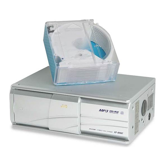
JVC CH-X1500 Schematic Diagrams
Hide thumbs
Also See for CH-X1500:
- Service manual (65 pages) ,
- Instructions manual (19 pages) ,
- Schematic diagrams (8 pages)

Related Manuals for JVC CH-X1500


Summary of Contents for JVC CH-X1500
- Page 1 CH-X1500 SCHEMATIC DIAGRAMS CD CHANGER CH-X1500 CD-ROM No.SML200301 Area Suffix Northern America Continental Europe Other Areas Contents Block diagram Standard schematic diagrams Printed circuit boards 2-6,7 No.49776 COPYRIGHT 2003 VICTOR COMPANY OF JAPAN, LTD. Jan. 2003...
- Page 2 Safety precaution Burrs formed during molding may be left over on some parts of the chassis. Therefore, pay attention to such burrs in the case of preforming repair of this system. Please use enough caution not to see the beam directly or touch it in case of an adjustment or operation check.
- Page 3 CH-X1500 Block diagram...
- Page 4 CH-X1500 CH-X1500 Standard schematic diagrams Main section (1) CN902 QNZ0095-001 R155 3.9K C151 C154 R151 R153 R162 C161 R546 330K 4.7K 2.2K 10/16 470P R548 10/16 C152 R152 R154 CDL+ 4.7K 2.2K 10/16 R550 R262 C261 10/16 C157 C252 R252...
- Page 5 CH-X1500 CDRW Main sction (2) C611 R613 R611 R610 R614 R612 C610 POS+ R601 POS- R602 R603 330k R604 330k L653 C603 C605 100/6.3 R608 S602 VSH1173-001 0.0068 S603 VSH1173-001 C675 C614 0.01 S604 VSH1173-001 47/6.3 Q601 2SB1132/QR/ TRAYOUT REST...
- Page 6 CH-X1500 CH-X1500 Printed circuit baords Main board (forward side) Main board (reverse side) CN501 C604 C907 CN601 CN904 CN501 C508 CN904 CN601 C162 C163 Q161 R615 R613 D981 C262 Q261 R610 Q981 R261 C601 C601 Q981 C606 C602 C261 C261...
- Page 7 < M E M O >...
- Page 8 CH-X1500 VICTOR COMPANY OF JAPAN, LIMITED AV & MULTIMEDIA COMPANY 10-1,1Chome,Ohwatari-machi,Maebashi-city,371-8543,Japan Printed in Japan 200301 (No.49776SCH)
Need help?
Do you have a question about the CH-X1500 and is the answer not in the manual?
Questions and answers