
Related Manuals for Motorola EVX S24


Summary of Contents for Motorola EVX S24
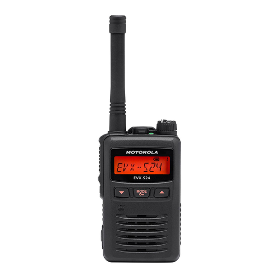
- Page 1 EVX S24 Service Manual JANUARY 2021 *MN006437A01* MN006437A01-AB © 2021 Motorola Solutions, Inc. All rights reserved...
-
Page 2: Table Of Contents
MN006437A01-AB Contents Contents Chapter 1: Introduction.....................3 Chapter 2: Specifications : USA (NA)..............4 Chapter 3: Exploded View and Miscellaneous Parts..........6 3.1 Parts List..........................8 3.2 Block Diagram (FR028210D)....................9 3.3 Block Diagram (PC003006A01).....................11 Chapter 4: Circuit Description................13 4.1 Receiver System........................13 4.2 Transmitter System........................13 4.3 PLL Frequency Synthesizer....................14 Chapter 5: Alignment....................15 5.1 Required Test Equipment...................... -
Page 3: Chapter 1: Introduction
MN006437A01-AB Introduction Chapter 1 Introduction This manual provides the technical information necessary for servicing the EVX-S24 UHF Digital/ Analog Transceiver. Servicing this equipment requires expertise in handing surface-mount chip components. Attempts by non-qualified persons to service this equipment may result in permanent damage not covered by the warranty, and may be illegal in some countries. -
Page 4: Chapter 2: Specifications : Usa (Na)
MN006437A01-AB Chapter 2: Specifications : USA (NA) Chapter 2 Specifications : USA (NA) NOTICE: Specifications subject to change without notice or obligation. Table 1: General Frequency range: 403-480 MHz Channel/Group: 256 Channels / 16 Groups Emission Type: 7K60F1E / 7K60FXE (Digital: 12.5 kHz Voice) 7K60F1D / 7K60FXD (Digital: 12.5 kHz Data) 7K60F1W (Digital: Combination of 12.5 kHz Voice &... - Page 5 MN006437A01-AB Chapter 2: Specifications : USA (NA) Conducted Spurious: –57 dBm Audio output: 500 mW @4 Ohm, <10 % THD Table 3: Transmitter (Measured by TIA/EIA-603) Output Power: 3/1/0.5 W (Digital) 2/1/0.5 W (Analog) Modulation: Sigma Delta Modulation Maximum Frequency Deviation: ±5.0 kHz (25 kHz Step, Analog) ±2.5 kHz (12.5 kHz Step, Analog) Conducted Spurious Emissions:...
-
Page 6: Chapter 3: Exploded View And Miscellaneous Parts
MN006437A01-AB Chapter 3: Exploded View and Miscellaneous Parts Chapter 3 Exploded View and Miscellaneous Parts... - Page 7 MN006437A01-AB Chapter 3: Exploded View and Miscellaneous Parts FRONT CASE ASSY O RING ( PANEL ) FRONT CASE ASSY ( C OMPORNENT RA1631000 PANEL ASSY ( FRONT ) – SPEAKER – SP NET O RING ( PANEL ) KEYPAD WINDOW ( C146 ) DOUBLE FASE ADHESIVE ( WDO ) MIC MEMBRANE PAD ( WINDOW )
-
Page 8: Parts List
MN006437A01-AB Chapter 3: Exploded View and Miscellaneous Parts Parts List REF. DESCRIPTION VALUE MFR’s DESIG VXSTD P/N SIDE LAY ADR CB7188000 FRONT CASE ASSY ( PANEL ) O RING RA1631000 REAR CASE ASSY CB7119000 ( TX/RX ) LIGHT GUIDE RA1632300 ( MICROTEX C012 ) SHEET RA0337300... -
Page 9: Block Diagram (Fr028210D)
MN006437A01-AB Chapter 3: Exploded View and Miscellaneous Parts Block Diagram (FR028210D) - Page 10 MN006437A01-AB Chapter 3: Exploded View and Miscellaneous Parts...
-
Page 11: Block Diagram (Pc003006A01)
MN006437A01-AB Chapter 3: Exploded View and Miscellaneous Parts Block Diagram (PC003006A01) - Page 12 MN006437A01-AB Chapter 3: Exploded View and Miscellaneous Parts...
-
Page 13: Chapter 4: Circuit Description
MN006437A01-AB Circuit Description Chapter 4 Circuit Description Receiver System Front-End RF Amplifier Incoming RF signal from the antenna passes through the low-pass filter, antenna switching diode D1011/D1014 (both 1SS390), and band-pass filter. The filtered RF signal is applied to the amplifier Q1033 (MAX2373ETC+T), then remove the undesired frequen- cies by another band-pass filter. -
Page 14: Pll Frequency Synthesizer
MN006437A01-AB Chapter 4: Circuit Description PLL Frequency Synthesizer The frequency synthesizer consists of VCO, TCXO X1001, and the custom IC Q1046 (RODINIA). The output frequency from TCXO X1001 is 19.2 MHz and the tolerance is ±1.5 ppm in the temperature range –22 °F to +140 °F (–30 °C to +60 °C). -
Page 15: Chapter 5: Alignment
MN006437A01-AB Alignment Chapter 5 Alignment The EVX-S24 is carefully aligned at the factory for the specified performance across the frequency range specified for each version. Realignment should therefore not be necessary except in the event of a component failure, or altering version type. All component replacement and service should be performed only by an authorized Vertex Standard representative, or the warranty policy may be void. -
Page 16: Alignment Preparation And Precautions
MN006437A01-AB Chapter 5: Alignment Alignment Preparation and Precautions A 50-Ohm RF Dummy Load and in-line wattmeter must be connected to the main antenna jack in all procedures that call for transmission, except where specified otherwise. Correct alignment is not possible with an antenna. Because of the BTL (Bridged Trans Less) Amplifier circuit used in the EVX-S24, do not connect earth side of the speaker leads to chassis “ground”. -
Page 17: Action Of The Switches
MN006437A01-AB Chapter 5: Alignment 5.4.1.1 Action of the Switches When the transceiver is in the “Alignment mode,“ the action of the PTT and all Programmable keys are ignored. All of the action is controlled by the PC. CAUTION: Please never turn off the power supply during alignment. If the power supply is turned off during alignment, the alignment data will be corrupted. -
Page 18: Alignment Mode
MN006437A01-AB Chapter 5: Alignment 5.4.1.2 Alignment Mode In the “Alignment Mode”, the aligned data written in the radio will be able to re-align its alignment data. The value of each parameter can be changed to desired position by "←"/"→" arrrow key for data up/ down, "↑"/"↓"... -
Page 19: Pll Reference Frequency (Frequency)
MN006437A01-AB Chapter 5: Alignment 2 Click the “CH” button on the desired channel. The RX VCO status (“Lock” or “Unlock”) will appear in the “RX” box. 3 Click the “PTT” button. The radio starts to transmit on the selected channel, and the TX VCO status (“Lock”... -
Page 20: Tx Power
MN006437A01-AB Chapter 5: Alignment 2 Click the “PTT” button or press the “SPACE” bar of the computer’s keyboard, the radio will start to transmit on the center frequency channel. 3 Set the value to get the desired frequency according to the following ways: •... - Page 21 MN006437A01-AB Chapter 5: Alignment 2 Click the “PTT” button on the desired channel. The radio starts to transmit on the selected channel. 3 Set the value to get desired output power (High Pwr: 3 W, Low3 Pwr: 2 W, Low2 Pwr: 1 W, Low1 Pwr: 0.5 W) on the Power Meter according to the following ways: •...
-
Page 22: Maximum Deviation (Wide/Narrow)
MN006437A01-AB Chapter 5: Alignment 5.4.5 Maximum Deviation (Wide/Narrow) This parameter is to align the “Maximum Deviation” (Wide/Narrow). Procedure: 1 Press the “Max Dev (W/N)” button to open the “Max Deviation Alignment” window. 2 Click the “PTT” button on the desired channel. The radio starts to transmit on the selected channel. -
Page 23: Symbol Deviation
MN006437A01-AB Chapter 5: Alignment 2 You may select the alignment type from the “Radio” button (ADJ Type) located at the bottom of the screen, as needed. Basic “Low-edge / band center / high-edge” and select the channel for alignment (Default). Single Alignment value changes only on the selected channel. -
Page 24: Ctcss Deviation (Wide/Narrow)
MN006437A01-AB Chapter 5: Alignment • Pressing the up-down key of the computer’s keyboard • Entering the value (“0000” - “FFFF”) in the entry box from the computer’s keyboard. 4 After getting the desired deviation, click the “PTT” button or press the “SPACE” bar to stop transmitting. -
Page 25: Dcs Deviation (Wide/Narrow)
MN006437A01-AB Chapter 5: Alignment 4 After getting the desired deviation, click the “PTT” button or press the “SPACE” bar to stop transmitting. 5 Click the “OK” button to finish the CTCSS Deviation alignment and save the data. You may align the deviation level by any CTCSS tone frequency (default: 300.0 Hz) by changing the value of the “CTCSS Freq”... -
Page 26: Dtmf Deviation
MN006437A01-AB Chapter 5: Alignment 5.4.9 DTMF Deviation Procedure: 1 Press the “DTMF” button to open the “DTMF Deviation Alignment” window. 2 Click the “PTT” button or press the “SPACE” bar of the computer’s keyboard to transmit the radio. 3 Set the value to get desired deviation (Nominal: 3.0 kHz) on the deviation meter according to the following ways: •... -
Page 27: Sequential Tone Deviation
MN006437A01-AB Chapter 5: Alignment 2 Click the “PTT” button or press the “SPACE” bar of the computer’s keyboard to transmit the radio. 3 Set the value to get desired deviation (Nominal: 3.0 kHz) on the deviation meter according to the following ways: •... -
Page 28: Download (Save) The Alignment Data And Exit From The Alignment Mode
MN006437A01-AB Chapter 5: Alignment 2 Entering the desired value in the “New” box from the computer’s keyboard. 3 Click the “OK” button to finish the Sequential Tone Deviation alignment and save the data. 5.4.12 Download (Save) the Alignment Data and Exit From the Alignment Mode Procedure: Press the “OK”... -
Page 29: Chapter 6: Main Unit (Fr028210D)
MN006437A01-AB Main Unit (FR028210D) Chapter 6 Main Unit (FR028210D) Figure 1: Circuit Diagram (RF Section) - Page 30 MN006437A01-AB Chapter 6: Main Unit (FR028210D) Figure 2: Circuit Diagram (CONTROL Section)
- Page 31 MN006437A01-AB Chapter 6: Main Unit (FR028210D) Figure 3: Parts Layout (Side “A”)
- Page 32 MN006437A01-AB Chapter 6: Main Unit (FR028210D) Figure 4: Parts Layout (Side “B”)
-
Page 33: Main Unit Parts List (Fr028210D)
MN006437A01-AB Chapter 6: Main Unit (FR028210D) Main Unit Parts List (FR028210D) DESCRIPTION VALUE TOL. MFR'S DESIG VXSTD P/N TYPE SIDE LAY ADR PCB with Component CB7203000 C 1001 CHIP CAP. 0.1uF GRM155B11A104KA01D K22108802 C 1002 CHIP CAP. 0.1uF GRM155B11A104KA01D K22108802 C 1003 CHIP CAP. - Page 34 MN006437A01-AB Chapter 6: Main Unit (FR028210D) DESCRIPTION VALUE TOL. MFR'S DESIG VXSTD P/N TYPE SIDE LAY ADR C 1098 CHIP CAP. 0.001uF GRM155B11H102KA01D K22178809 C 1100 CHIP CAP. 100pF GRM1552C1H101JA01D K22178236 C 1102 CHIP CAP. 0.001uF GRM155B11H102KA01D K22178809 C 1104 CHIP CAP.
- Page 35 MN006437A01-AB Chapter 6: Main Unit (FR028210D) DESCRIPTION VALUE TOL. MFR'S DESIG VXSTD P/N TYPE SIDE LAY ADR C 1192 CHIP CAP. 56pF GRM0332C1H560JA01D K22177521 C 1193 CHIP CAP. 100pF GRM1552C1H101JA01D K22178236 C 1194 CHIP CAP. 390pF GRM155B11H391KA01D K22178804 C 1195 CHIP CAP.
- Page 36 MN006437A01-AB Chapter 6: Main Unit (FR028210D) DESCRIPTION VALUE TOL. MFR'S DESIG VXSTD P/N TYPE SIDE LAY ADR C 1276 CHIP CAP. 0.1uF GRM155B11A104KA01D K22108802 C 1284 CHIP CAP. 0.1uF GRM155B11A104KA01D K22108802 C 1285 CHIP CAP. 0.1uF GRM155B11A104KA01D K22108802 C 1286 CHIP CAP.
- Page 37 MN006437A01-AB Chapter 6: Main Unit (FR028210D) DESCRIPTION VALUE TOL. MFR'S DESIG VXSTD P/N TYPE SIDE LAY ADR C 1610 CHIP CAP. 150pF GRM033B11E151KA01D K22147702 C 1611 CHIP CAP. 150pF GRM033B11E151KA01D K22147702 C 1612 CHIP CAP. 150pF GRM033B11E151KA01D K22147702 C 1613 CHIP CAP.
- Page 38 MN006437A01-AB Chapter 6: Main Unit (FR028210D) DESCRIPTION VALUE TOL. MFR'S DESIG VXSTD P/N TYPE SIDE LAY ADR D 1030 DIODE 1SV280(TPH3.F) G2070550 D 1031 DIODE 1SV280(TPH3.F) G2070550 D 1032 DIODE 1SV279(TPH3.F) G2070618 D 1035 BRGB1313F-TR G2071396 D 1036 DIODE RB751S40T1G G2070850 D 1037 DIODE...
- Page 39 MN006437A01-AB Chapter 6: Main Unit (FR028210D) DESCRIPTION VALUE TOL. MFR'S DESIG VXSTD P/N TYPE SIDE LAY ADR J 1002 CONTACT 10F00B35011-P P0091593 J 1003 CONNECTOR ZX62D-B-5PA8(30) P1091565 J 1004 CONNECTOR 47410-0001 P0091591 J 1005 CONNECTOR 03-A70G0-36BKA P1091581 J 1008 CONNECTOR FH34SRJ-20S-0.5SH(50) P1091573 J 1009...
- Page 40 MN006437A01-AB Chapter 6: Main Unit (FR028210D) DESCRIPTION VALUE TOL. MFR'S DESIG VXSTD P/N TYPE SIDE LAY ADR Q 1041 TRANSISTOR 2SC5010-T1-A/YFB G3350108 Q 1042 TRANSISTOR UMC5N TR G3070137 Q 1043 TRANSISTOR DTC143EE TL G3070114 Q 1044 TRANSISTOR DTC143EE TL G3070114 Q 1045 2SK880GR(TE85R.F) G3808807G...
- Page 41 MN006437A01-AB Chapter 6: Main Unit (FR028210D) DESCRIPTION VALUE TOL. MFR'S DESIG VXSTD P/N TYPE SIDE LAY ADR R 1051 CHIP RES. 1/16W 1% RMC1/16SK101FTH J24189504 R 1052 CHIP RES. 2.2M 1/16W 0.5% RGC1/16SK225DTH J24189599 R 1053 CHIP RES. 1/16W 1% RMC1/16SK471FTH J24189512 R 1055...
- Page 42 MN006437A01-AB Chapter 6: Main Unit (FR028210D) DESCRIPTION VALUE TOL. MFR'S DESIG VXSTD P/N TYPE SIDE LAY ADR R 1152 CHIP RES. 1/16W 5% RMC1/16S JPTH J24189070 R 1153 CHIP RES. 1/16W 1% RMC1/16SK101FTH J24189504 R 1154 CHIP RES. 1/16W 5% RMC1/16S JPTH J24189070 R 1157...
- Page 43 MN006437A01-AB Chapter 6: Main Unit (FR028210D) DESCRIPTION VALUE TOL. MFR'S DESIG VXSTD P/N TYPE SIDE LAY ADR R 1250 CHIP RES. 1/16W 1% RMC1/16SK103FTH J24189489 R 1251 CHIP RES. 1/16W 1% RMC1/16SK103FTH J24189489 R 1252 CHIP RES. 1/16W 5% RMC1/16 000JATP J24185000 R 1253 CHIP RES.
- Page 44 MN006437A01-AB Chapter 6: Main Unit (FR028210D) DESCRIPTION VALUE TOL. MFR'S DESIG VXSTD P/N TYPE SIDE LAY ADR R 1372 CHIP RES. 1/16W 1% RMC1/16SK101FTH J24189504 R 1374 CHIP RES. 1/16W 5% RMC1/16S 120JTH J24189002 R 1377 CHIP RES. 1/16W 1% RMC1/16SK103FTH J24189489 R 1601...
-
Page 45: Chapter 7: Display Unit (Fr028310A)
MN006437A01-AB Display Unit (FR028310A) Chapter 7 Display Unit (FR028310A) - Page 46 MN006437A01-AB Chapter 7: Display Unit (FR028310A) Figure 5: Display Unit (FR028310A)
- Page 47 MN006437A01-AB Chapter 7: Display Unit (FR028310A) Figure 6: Parts Layout (Side “A”)
- Page 48 MN006437A01-AB Chapter 7: Display Unit (FR028310A) Figure 7: Parts Layout (Side “B”)
-
Page 49: Display Unit Parts List
MN006437A01-AB Chapter 7: Display Unit (FR028310A) Display Unit Parts List DESCRIPTION VALUE TOL. MFR'S DESIG VXSTD P/N TYPE SIDE LAY ADR CB7125000 ( BLK ) PCB with Component C 2002 CHIP CAP. 0.001uF GRM155B11H102KA01D K22178809 C 2003 CHIP CAP. 470pF GRM1882C1H471JA01D K22174249 C 2004... -
Page 50: Chapter 8: Main Unit (Pc003006A01)
MN006437A01-AB Chapter 8: Main Unit (PC003006A01) Chapter 8 Main Unit (PC003006A01) Figure 8: Circuit Diagram (RF Section) R1329 C1341 0.01 C1342 J1011 D1002 0603ESDA2 D1065 D1047 TX_ANT_EN C1004 R1005 D1003 UDZV16B C1278 1SS400G 470p UDZV6.2B F1003 C1009 (1608) FB1002 2.0A D1001 D1066 L9190127... - Page 51 MN006437A01-AB Chapter 8: Main Unit (PC003006A01) Figure 9: Circuit Diagram (CONTROL Section) C1601 B 6.3V C1603 C1602 R1601 R1602 1/20W 1/20W R1603 R1604 49.9 R1607 2.2K R1608 2.2K R1609 2.2K C1615 B 10V C1616 B 10V C1617 B 10V R1612 C1618 2.2K B 10V...
- Page 52 MN006437A01-AB Chapter 8: Main Unit (PC003006A01) Figure 10: Parts Layout (Top) OVERLAY_TOP...
- Page 53 MN006437A01-AB Chapter 8: Main Unit (PC003006A01) Figure 11: Parts Layout (Bottom)
-
Page 54: Main Unit Parts List (Pc003006A01)
MN006437A01-AB Chapter 8: Main Unit (PC003006A01) Main Unit Parts List (PC003006A01) DESCRIPTION VALUE TOL. MFR'S DESIG Part No. SIDE LAY ADR C1001 CHIP CAP. 0.1uF OBS-LMK105BJ104KV-F K22108802 C1002 CHIP CAP. 0.1uF OBS-LMK105BJ104KV-F K22108802 C1003 CHIP CAP. 0.1uF OBS-LMK105BJ104KV-F K22108802 C1004 CHIP CAP. - Page 55 MN006437A01-AB Chapter 8: Main Unit (PC003006A01) DESCRIPTION VALUE TOL. MFR'S DESIG Part No. SIDE LAY ADR C1060 CHIP CAP. 10uF 12063C106KAT2A K22141815 C1061 CHIP CAP. 0.022uF GRM155B11C223KA01D K22128806 C1062 CHIP CAP. 0.0022uF GRM155B11H222KA01D K22178813 C1066 CHIP CAP. 150pF GRM1552C1H151JA01D K22178240 C1067 CHIP CAP.
- Page 56 MN006437A01-AB Chapter 8: Main Unit (PC003006A01) DESCRIPTION VALUE TOL. MFR'S DESIG Part No. SIDE LAY ADR C1120 CHIP CAP. 4.7uF 6.3V JMK107BJ475KA-T K22084809 C1121 CHIP CAP. 4.7uF 6.3V JMK107BJ475KA-T K22084809 C1122 CHIP CAP. 4.7uF 6.3V JMK107BJ475KA-T K22084809 C1123 CHIP CAP. K22178292 K22178292 C1124...
- Page 57 MN006437A01-AB Chapter 8: Main Unit (PC003006A01) DESCRIPTION VALUE TOL. MFR'S DESIG Part No. SIDE LAY ADR C1190 CHIP CAP. 0.1uF K22107707 K22107707 C1191 CHIP CAP. 0.1uF K22107707 K22107707 C1192 CHIP CAP. 56pF GRM0332C1H560JA01D K22177521 C1193 CHIP CAP. 100pF GRM1552C1H101JA01D K22178236 C1194 CHIP CAP.
- Page 58 MN006437A01-AB Chapter 8: Main Unit (PC003006A01) DESCRIPTION VALUE TOL. MFR'S DESIG Part No. SIDE LAY ADR C1239 CHIP CAP. 0.1uF K22107707 K22107707 C1240 CHIP CAP. OBS-LMK105BJ105KV-F K22108809 C1241 CHIP CAP. 0.1uF K22107707 K22107707 C1242 CHIP CAP. OBS-LMK105BJ105KV-F K22108809 C1243 CHIP CAP. 0.001uF GRM033B11E102KA01D K22147712...
- Page 59 MN006437A01-AB Chapter 8: Main Unit (PC003006A01) DESCRIPTION VALUE TOL. MFR'S DESIG Part No. SIDE LAY ADR C1299 CHIP CAP. 0.001uF GRM155B11H102KA01D K22178809 C1305 CHIP CAP. 390pF GRM155B11H391KA01D K22178804 C1306 CHIP CAP. 390pF GRM155B11H391KA01D K22178804 C1307 CHIP CAP. 390pF GRM155B11H391KA01D K22178804 C1309 CHIP CAP.
- Page 60 MN006437A01-AB Chapter 8: Main Unit (PC003006A01) DESCRIPTION VALUE TOL. MFR'S DESIG Part No. SIDE LAY ADR C1372 CHIP CAP. 0.033uF K22108803 K22108803 C1373 CHIP CAP. 0.0068uF K22148803 K22148803 C1374 CHIP CAP. 150pF GRM1552C1H151JA01D K22178240 C1375 CHIP CAP. OBS-LMK105BJ105KV-F K22108809 C1377 CHIP TA.CAP.
- Page 61 MN006437A01-AB Chapter 8: Main Unit (PC003006A01) DESCRIPTION VALUE TOL. MFR'S DESIG Part No. SIDE LAY ADR C1642 CHIP CAP. 330pF GRM033B11E331KA01D K22147706 C1643 CHIP CAP. 330pF GRM033B11E331KA01D K22147706 C1644 CHIP CAP. 0.1uF K22107707 K22107707 C1645 CHIP CAP. 0.1uF K22107707 K22107707 C1646 CHIP CAP.
- Page 62 MN006437A01-AB Chapter 8: Main Unit (PC003006A01) DESCRIPTION VALUE TOL. MFR'S DESIG Part No. SIDE LAY ADR C1712 CHIP CAP. 0.1uF OBS-LMK105BJ104KV-F K22108802 C1713 CHIP CAP. 0.022uF GRM155B11C223KA01D K22128806 C1714 CHIP TA.CAP. 10uF K78120095 K78120095 C1715 CHIP TA.CAP. 10uF K78120095 K78120095 C1718 CHIP CAP.
- Page 63 MN006437A01-AB Chapter 8: Main Unit (PC003006A01) DESCRIPTION VALUE TOL. MFR'S DESIG Part No. SIDE LAY ADR D1059 DIODE 1SS400GT2R G2070934 D1061 DIODE 1SS400GT2R G2070934 D1062 DIODE 1SS400GT2R G2070934 D1065 DIODE 1SS400GT2R G2070934 D1066 DIODE 1SS400GT2R G2070934 D1067 DIODE 1SS400GT2R G2070934 D1068 DIODE 1SS400GT2R...
- Page 64 MN006437A01-AB Chapter 8: Main Unit (PC003006A01) DESCRIPTION VALUE TOL. MFR'S DESIG Part No. SIDE LAY ADR FB1601 FERRITE BEADS L9190127 L9190127 FB1602 FERRITE BEADS L9190127 L9190127 FB1603 FERRITE BEADS L9190127 L9190127 FB1604 FERRITE BEADS L9190127 L9190127 FB1605 FERRITE BEADS L9190127 L9190127 HS1001 PLATE...
- Page 65 MN006437A01-AB Chapter 8: Main Unit (PC003006A01) DESCRIPTION VALUE TOL. MFR'S DESIG Part No. SIDE LAY ADR L1035 M.RFC 0.022uH 0.02 L1691602 L1691602 L1036 M.RFC 0.015uH 0.02 0603HP-15NXGLW L1691600 L1037 M.RFC 0.22uH 0402HPH-R22XGLW L1691967 L1038 M.RFC 0.22uH 0402HPH-R22XGLW L1691967 L1039 M.RFC 0.0012uH 0.3nH HK10051N2S-T...
- Page 66 MN006437A01-AB Chapter 8: Main Unit (PC003006A01) DESCRIPTION VALUE TOL. MFR'S DESIG Part No. SIDE LAY ADR Q1049 TRANSISTOR 2SC4617TLR G3346178R Q1050 SN74AUC1GU04YZPR G1094915 Q1051 TRANSISTOR 2SC4617TLR G3346178R Q1052 RUM002N02GT2L G3070455 Q1053 TRANSISTOR 2SA1774TLR G3117748R Q1054 TS3USB221ARSER G1094963 Q1055 TRANSISTOR 2SA1774TLR G3117748R Q1057 TRANSISTOR...
- Page 67 MN006437A01-AB Chapter 8: Main Unit (PC003006A01) DESCRIPTION VALUE TOL. MFR'S DESIG Part No. SIDE LAY ADR R1019 CHIP RES. 1/2W 0.01 RLC32-R200FTP J24279031 R1020 CHIP RES. 1/2W 0.01 RLC32-R200FTP J24279031 R1021 CHIP RES. 2.2k 1/16W 0.01 RMC1/16SK222FTH J24189497 R1022 CHIP RES. 1/16W 0.05 RMC1/16SJPTH...
- Page 68 MN006437A01-AB Chapter 8: Main Unit (PC003006A01) DESCRIPTION VALUE TOL. MFR'S DESIG Part No. SIDE LAY ADR R1079 CHIP RES. 8.2k 1/16W 0.01 J24189522 J24189522 R1080 CHIP RES. 2.2k 1/16W 0.01 RMC1/16SK222FTH J24189497 R1082 NOTPLACED A R1083 CHIP RES. 4.7k 1/16W 0.01 RMC1/16SK472FTH J24189488...
- Page 69 MN006437A01-AB Chapter 8: Main Unit (PC003006A01) DESCRIPTION VALUE TOL. MFR'S DESIG Part No. SIDE LAY ADR R1138 CHIP RES. 1/16W 0.01 RMC1/16SK221FTH J24189508 R1140 CHIP RES. 2.7k 1/16W 0.01 RMC1/16SK272FTH J24189517 R1141 CHIP RES. 2.7k 1/16W 0.01 RMC1/16SK272FTH J24189517 R1146 CHIP RES.
- Page 70 MN006437A01-AB Chapter 8: Main Unit (PC003006A01) DESCRIPTION VALUE TOL. MFR'S DESIG Part No. SIDE LAY ADR R1208 CHIP RES. 1/20W 0.05 RMC1/20JPPA J24175000 R1209 CHIP RES. 1/20W 0.05 RMC1/20JPPA J24175000 R1210 CHIP RES. 1/20W 0.05 RMC1/20JPPA J24175000 R1211 CHIP RES. 1/20W 0.05 RMC1/20JPPA...
- Page 71 MN006437A01-AB Chapter 8: Main Unit (PC003006A01) DESCRIPTION VALUE TOL. MFR'S DESIG Part No. SIDE LAY ADR R1262 CHIP RES. 220k 1/16W 0.01 J24189533 J24189533 R1263 CHIP RES. 2.2M 1/16W 0.005 RGC1/16SK225DTH J24189599 R1266 CHIP RES. 4.7k 1/16W 0.01 RMC1/16SK472FTH J24189488 R1269 CHIP RES.
- Page 72 MN006437A01-AB Chapter 8: Main Unit (PC003006A01) DESCRIPTION VALUE TOL. MFR'S DESIG Part No. SIDE LAY ADR R1349 CHIP RES. 1/16W 0.05 RMC1/16SJPTH J24189070 R1351 CHIP RES. 4.7k 1/16W 0.01 RMC1/16SK472FTH J24189488 R1352 CHIP RES. 4.7k 1/16W 0.01 RMC1/16SK472FTH J24189488 R1353 CHIP RES.
- Page 73 MN006437A01-AB Chapter 8: Main Unit (PC003006A01) DESCRIPTION VALUE TOL. MFR'S DESIG Part No. SIDE LAY ADR R1630 CHIP RES. 1/16W 0.05 RMC1/16S-220JTH J24189005 R1631 CHIP RES. 1/16W 0.05 RMC1/16SJPTH J24189070 R1632 CHIP RES. 1/16W 0.05 RMC1/16SJPTH J24189070 R1633 CHIP RES. 1/16W 0.05 RMC1/16SJPTH...
- Page 74 MN006437A01-AB Chapter 8: Main Unit (PC003006A01) DESCRIPTION VALUE TOL. MFR'S DESIG Part No. SIDE LAY ADR T1001 CHOKE COIL L1691717 L1691717 TH1001 THERMISTOR G9090150 G9090150 U1700 TPA6211A1DRBR 5188032U16 U1701 MAX20327EWL+T LN001205A01 A VR1001 POT. TP76N975N13.5FB503RY10034 J60800314 VR1700 DIODE PESD5V0S1BL,315 4875179M01 VR1701 DIODE PESD5V0S1BL,315...
Need help?
Do you have a question about the EVX S24 and is the answer not in the manual?
Questions and answers