Table of Contents
Advertisement
Quick Links
Advertisement
Table of Contents

Related Manuals for Casio SF-5300E


Summary of Contents for Casio SF-5300E
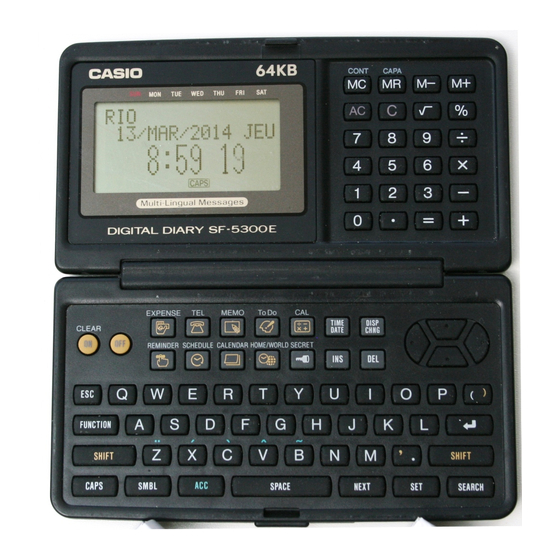
- Page 1 (with price) SF-5300E (LX-551AQ) JAN. 1995 SF-5300E...
-
Page 2: Table Of Contents
CONTENTS SCHEMATIC DIAGRAM 1-1. MAIN PCB .......................1 1-2. KEY MATRIX 1......................2 1-3. KEY MATRIX 2......................3 SPECIFICATIONS 2-1. General ........................5 2-2. Function .........................5 2-3. Storage Capacitiy ....................9 GENERAL GUIDE 3-1. Outward ........................10 3-2. About data errors ....................10 3-3. About the memory overflow message ...............10 3-4. - Page 3 1. SCHEMATIC DIAGRAM 1-1. MAIN PCB — 1 —...
-
Page 4: Key Matrix 1
1-2. KEY MATRIX 1 — 2 —... - Page 5 1-3. KEY MATRIX 2 ÷ M– – CODE:02 CODE:03 CODE:07 CODE:11 CODE:15 CODE:19 CODE:23 CODE:01 CODE:06 CODE:10 CODE:14 CODE:18 CODE:22 CODE:00 CODE:05 CODE:09 CODE:13 CODE:17 CODE:04 CODE:08 CODE:12 CODE:16 CODE:20 CODE:21 — 3 —...
-
Page 6: Specifications
2. SPECIFICATIONS 2-1. General 16-column × 4-line LCD Display element: Memory capacity: 64 kB (60972 bytes) Main component: Power supply: 2 lithium batteries (CR2032) Power consumption: 0.05 W Battery life: * Approximately 400 hours continuous operation in Telephone Directory Approximately 350 hours repeating one minute of input and 10 minutes of display in Telephone Directory Approximately 12 months for memory backup * The batteries that have been installed in this unit when user purchased it are for the factory test, so it will... - Page 7 Keys: Key Cap Name Function Accent key Use this key to input accented characters. Calculator Mode key Press this key to enter the Calculator Mode. CALENDAR Calendar key Press this key to enter the Calendar Mode. CAPA Capacity key Hold down this key to display the current status of the memory.
- Page 8 Key Cap Name Function Off key Press this key to switch power off. ON CLEAR Power On/Clear key • Press this key to switch power on. • Press this key to clear the display. REMINDER Reminder Mode key Press this key to enter the Reminder Mode. SCHEDULE Schedule Mode key Press this key to enter the Schedule Keeper.
- Page 9 Auto Sort Sequence: Telephone Directory data items are automatically sorted in alphabetical order according to the first letter in the NAME entry. The following table shows the sequence used for data sorts. § â (space) > ê æ î ç ”...
-
Page 10: Storage Capacitiy
2-3. Storage Capacitiy The 64K bytes memory capacity includes a 60972 bytes user area. The following shows examples of what this means for the storage of data in each mode. Telephone Directory Approximately 2903, under the following conditions: 8-character name 10- character telephone number Approximately 1451, under the following conditions: 8-character name... -
Page 11: General Guide
3. GENERAL GUIDE 3-1. Outward Display Mode Keys Numeric Keys Power OFF Power ON/ Cursor Keys Clear Key Keyboard Connector Terminal Lock 3-2. About data errors Whenever you switch on the power of the SF Unit, it performs a self-check before beginning operation. -
Page 12: Mesage Table
3-4. Message Table Message Meaning Action NO DATA! Search operation attempted when Current search operation no data is stored in memory. cannot be performed. NOT FOUND! Data specified in search operation Change specification or cancel does not exist in memory. search. -
Page 13: To Select A Mode
3-6. To select a mode Press one of the mode keys to select the mode you want. EXPENSE The Expense Mode lets you store expense data, including payment date, payment method, description, etc. You can also produce total for a specific period of time. -
Page 14: To Switch The Key Input And Alarm Tones On And Off
Just like in the above example display, all of the functions included in a function menu have a number at the beginning. Press the number key that corresponds to the function you want to perform. Whenever a function menu item's leading number is replaced by " ", it means you can't select that menu item in the operation you are performing. -
Page 15: Replacing The Batteries
4. REPLACING THE BATTERIES Loosen the screw on the back of the unit that holds the battery compartment cover in place, and remove the cover. Screw Loosen the screw that secures one of the two battery holders in place and remove the battery holder. RESET Caution:Be sure to remove only one battery at a time. -
Page 16: Resetting The Unit
5. RESETTING THE UNIT The following procedures erase all data stored in the memory of the unit. RESET Button RESET Turn on the unit and press the RESET button with a thin, pointed object. ALL DATA CLEAR! CAPS Press Y to reset the memory and delete all data, or N to abort the reset operation without deleting anything. -
Page 17: Saving Data
6. SAVING DATA The SF-5300E can transfer the customer's data (both the open and secret areas) to another SF-5300E. • Turn off both the transmitting and receiving units and connect them using the SB-60/62 cable. SB-60/62 1 Setting up the receiving unit: 1. - Page 18 3. Press , and FUNC twice. MENU * If the password isn't registered in the SF-5300E, 1* TO SECRET AREA the display shows instead ALL DELETE of "1." LABEL EDIT DATA COMM CAPS 4. Press to select DATA COMM. SEND RECEIVE SET UP PAR.
- Page 19 Bit length: 7 BPS: 9600 1. Press , and MENU 2. Press FUNC twice. * If the password isn't registered in the SF-5300E, 1* TO SECRET AREA the display shows instead ALL DELETE of "1." LABEL EDIT DATA COMM CAPS 3.
- Page 20 6. Press to select SEND. ONE ITEM MODE DATA ALL DATA - SEND - CAPS 7. Press to select ALL DATA. SEND ALL DATA? SET/ESC CAPS 8. Press to start data transmission or to abort the operation without sending anything. SENDING DATA TO STOP...
-
Page 21: Lsi Pin Functions
7. LSI PIN FUNCTIONS 7-1. CPU: LSI1 No.1 Pin No. Name Description 1 ~ 5 C0 ~ 4 Common signal for display GND 0 V BZ1,2 Buzzer terminal Power supply terminal (+5.3 V) CSRA1 Chip enable signal for LSI3 CSRA2 Chip enable signal for LSI2 CSROM Chip enable signal for LSI4... -
Page 22: Ram:lsi2 And Lsi3 (Cxk58257)
Pin No. Name Description 64,65 OSC I/O Clock terminal 67,69~71 V1 ~ 4 Voltage for LCD drive OFF: 0 V ON– V1: 0.64 Minimum ~ 1.29 Maximum V V2: 1.29 Minimum ~ 2.56 Maximum V V3: 3.99 Minimum ~ 2.71 Maximum V V4: 4.64 Minimum ~ 3.99 Maximum V Not used INTO... -
Page 23: Rom:lsi4 ( Μ Pd23C1001Eagz)
µ 7-3. ROM: LSI4 ( PD23C1001EAGZ) DC/PGM_ NC/VPP Pin No. Name Description 1~5,12,13,16~24,39 A0~16 Address bus 25,28,29,31~33,36,37 D0~7 Data bus 6,15,26,35 7,14,27,34 Not used 9~11 DC/PGM_,VCC,NC/VPP Power supply terminal (+5.3 V) GND 0 V Chip enable signal from LSI1 — —... -
Page 24: Voltage Regulator:reg1 (S-81253)
7-4. VOLTAGE REGULATOR: REG1 (S-81253) Output Voltage (VDD): 5.3 V ± 5% – 7-5. VOLTAGE DETECTOR: DET1 (RH5VL46CA) Input Voltage (VCC) Output Voltage (OUT) VCC > 5.2 V 5.2 V VCC < 5.2 V — —... -
Page 25: Troubleshooting
8. TROUBLESHOOTING No power on START Adjust the display contrast. Is the display contrast adjustment OK? Replace the batteries. Are the power of batteries strong enough? Does the display appear by pressing Check another function. the reset button? Does the unit sound with each key entry? Refer to "No/Erratic Display."... - Page 26 Is Pin 1 of DET1 5.2 V? Replace DET1. Is Pin 11 of LSI1 sending the signal? Replace LSI1. Is Pin 13 of LSI1 sending the signal? Replace LSI1. Is the soldering of LSI2, LSI3 or LSI4 poor? Resolder. Replace LSI1, LSI2, LSI3, or LSI4. No key input START Does the rubber key contact make positive...
- Page 27 No/Erratic display START Replace the batteries. Are the power of batteries strong enough? Adjust the contact and clean Is input Pin 2 of REG1 6 V? the battery springs. Replace REG1. Is output Pin 3 of REG1 5.3 V? Are the voltages of V1, V2, V3, and V4 strong enough? V1: 1.3 V Replace C1, C2, C3, or C4.
-
Page 28: Diagnostics
9. DIAGNOSTICS Notes: 1. Be sure to transfer data to another SF-5300E unit before entering the diagnostic mode, because the data will be changed by entering the diagnostic mode. 2. The shorting pads shown in the following illustration are covered by a blind label. - Page 29 Display Check Operation Display Note Display check Press 1 on the TEST MENU. DISP RVS. WHITE 5 FRAME To return to the BLACK 6 DOT4 TEST MENU, CHECK. 7 TIME press No display All dots displayed Checker displayed SEARCH ACC CAPS SHIFT Reverse checker display Frame display...
- Page 30 Operation Display Note Shows dots at corners. Check timer. TIME DISPLAY 00:00:XX TEST 2 MEMORY MENU 3 KEY 4 BUZZER DISP 5 I/F Memory Check The functions of the numbered items on the display include: 1. Writes the test pattern in the ROM to the RAM area. (Test pattern1: Incremental order 00, 01, and so on) 2.
- Page 31 Operation Display Note MEMORY 3 WR2 (After a few seconds) 4 READ2 5 DUMP READ1 6 CHKSUM EXECUTING!! ( or 4 ) Normal COMPLETE!! 64KB RAM error DATA ERROR!! ADDRESS CORR If the displayed address XXXX is within 0000-7FFF, check LSI3. If the displayed address is within 8000-FFFF, check LSI2.
- Page 32 In the auto mode, the key input sequence is limited so that the keys must be pressed in the order of the key code as mentioned below. If a key is pressed in the wrong order, the SF-5300E beeps. Operation...
- Page 33 Buzzer Check Operation Display Note Buzzer check Press 4 on the TEST MENU. BUZZER 1 BEEP 2 ALARM1 To return to the 3 ALARM2 TEST MENU, press Check the sound. ( or 2 , 3 ) EXECUTING!! To return to the BUZZER menu, press any key.
-
Page 34: Assembly View
10. ASSEMBLY VIEW DISASSEMBLY Lift off the hinge tape F, loose the three screws ] on the hinge E, then remove the hinge E. Loose the two screws \ on the lower case O. After lifting off the plate G at the lower right corner, loose the screw \ on the upper case H, and remove the lower case O. -
Page 35: Parts List
11. PARTS LIST FOB Japan Item Code No. Parts Name Specification N.R.Yen Unit Price CHIP ON BOARD BONDIN 6413 3720 Chip on board bondin DB22AX3F00U*1 2,750 (This assembly contains the following available elements.) C1~4,7,8,12~14 6511 7560 Chip capacitor CP001A432T8 9 20 C5,6 6511 7510 Chip capacitor CP018F602A7... - Page 36 FOB Japan Item Code No. Parts Name Specification N.R.Yen Unit Price 6412 3160 Heat seal FX201P50209 6412 3150 PCB DADB22XX309 6413 3640 Lower case (DIS) FABDB222044 6409 6120 Battery holder ECDB1011108 2 20 6409 6210 Battery change label HGC00001102 1 20 6412 3060 Battery cover FADDB221001 1 20...
- Page 37 MA0200651A...
Need help?
Do you have a question about the SF-5300E and is the answer not in the manual?
Questions and answers