Table of Contents
Advertisement
Advertisement
Table of Contents

Related Manuals for Casio SF-5300B


Summary of Contents for Casio SF-5300B
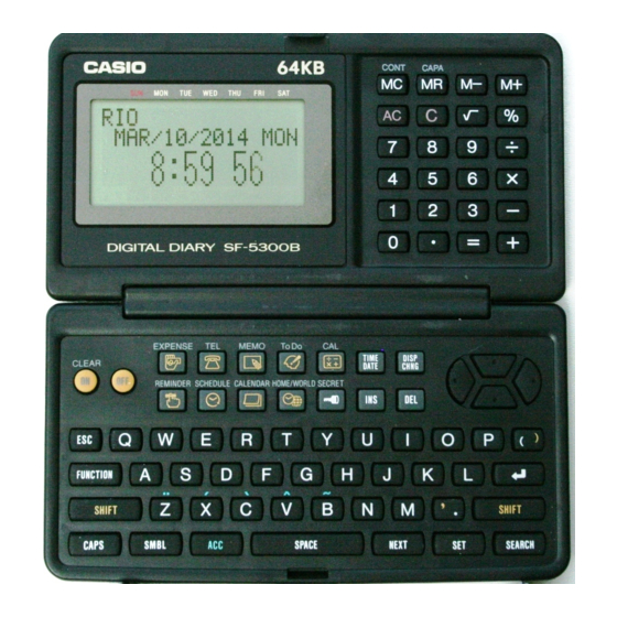
- Page 1 (with price) SF-5300B (LX-547) SEP. 1994 SF-5300B...
-
Page 2: Table Of Contents
CONTENTS 1. SCHEMATIC DIAGRAM 1-1. MAIN PCB ........................1 1-2. KEY MATRIX 1 ......................2 1-3. KEY MATRIX 2 ......................3 2. SPECIFICATIONS ......................5 3. REPLACING THE BATTERIES ..................6 4. RESETTING THE UNIT ....................7 5. SAVING DATA ........................8 6. LSI PIN FUNCTIONS 6-1. CPU:LSI1 .........................12 6-2. -
Page 3: Schematic Diagram
1. SCHEMATIC DIAGRAM 1-1. MAIN PCB — 1 —... -
Page 4: Key Matrix 1
1-2. KEY MATRIX 1 — 2 —... -
Page 5: Key Matrix 2
1-3. KEY MATRIX 2 ÷ M– – CODE:02 CODE:03 CODE:07 CODE:11 CODE:15 CODE:19 CODE:23 CODE:01 CODE:06 CODE:10 CODE:14 CODE:18 CODE:22 CODE:00 CODE:05 CODE:09 CODE:13 CODE:17 CODE:04 CODE:08 CODE:12 CODE:16 CODE:20 CODE:21 — 3 —... -
Page 6: Specifications
SPECIFICATIONS 16-column × 4-line LCD Display element: Memory capacity: 64 kB (60972 bytes) Main component: Power supply: 2 lithium batteries (CR2032) Power consumption: 0.05 W Battery life: Approximately 400 hours continuous operation in Telephone Directory Approximately 350 hours repeating one minute of input and 10 minutes of display in Telephone Directory Approximately 12 months for memory backup Auto power off:... -
Page 7: Replacing The Batteries
3. REPLACING THE BATTERIES Loosen the screw on the back of the SF-5300B that holds the battery compartment cover in place, and remove the cover. Screw Loosen the screw that secures one of the two battery holders in place and remove the battery holder. -
Page 8: Resetting The Unit
RESETTING THE UNIT The following procedures erase all data stored in the memory of the SF-5300B. RESET Button RESET 1. Turn on the unit and press the RESET button with a thin, pointed object. ALL DATA CLEAR! CAPS 2. Press Y to reset the memory and delete all data, or N to abort the reset operation without deleting anything. -
Page 9: Saving Data
SAVING DATA The SF-5300B can transfer the customer's data (both the open and secret areas) to another SF-5300B. • Turn off both the transmitting and receiving units and connect them using the SB-60/62 cable. SB-60/62 1 Setting up the receiving unit: 1. - Page 10 MENU FUNC Press , and twice. * If the password isn't 1* TO SECRET AREA registered in the SF-5300B, ALL DELETE the display shows instead of "1." LABEL EDIT DATA COMM CAPS Press to select DATA COMM. SEND RECEIVE SET UP PAR.
- Page 11 Parity: None Bit length: 7 BPS: 9600 Press , and MENU Press twice. FUNC * If the password isn't registered in the SF-5300B, 1* TO SECRET AREA the display shows instead ALL DELETE of "1." LABEL EDIT DATA COMM CAPS Press to select DATA COMM.
- Page 12 Press to select SEND. ONE ITEM MODE DATA ALL DATA - SEND - CAPS Press to select ALL DATA. SEND ALL DATA? SET/ESC CAPS Press to start data transmission or to abort the operation without sending anything. SENDING DATA TO STOP PRESS (ESC) CAPS •...
-
Page 13: Lsi Pin Functions
LSI PIN FUNCTIONS 6-1. CPU: LSI1 No.1 Pin No. Name Description 1 ~ 5 C0 ~ 4 Common signal for display GND 0 V BZ1,2 Buzzer terminal Power supply terminal (+5.3 V) CSRA1 Chip enable signal for LSI2 CSRA2 Chip enable signal for LSI3 CSROM Chip enable signal (Not used) Write enable signal for LSI2 and LSI3... -
Page 14: Ram:lsi2 And Lsi3 (Cxk58257)
Pin No. Name Description 64,65 OSC I/O Clock terminal 67,69~71 V1 ~ 4 Voltage for LCD drive OFF: 0 V ON– V1: 0.64 Minimum ~ 1.29 Maximum V V2: 1.29 Minimum ~ 2.56 Maximum V V3: 3.99 Minimum ~ 2.71 Maximum V V4: 4.64 Minimum ~ 3.99 Maximum V Not used INTO... -
Page 15: Voltage Regulator:reg1 (S-81253)
6-3. VOLTAGE REGULATOR: REG1 (S-81253) Output Voltage (VDD): 5.3 V ± 5% – 6-4. VOLTAGE DETECTOR: DET1 (RH5VL46CA) Input Voltage (VCC) Output Voltage (OUT) VCC > 5.2 V 5.2 V VCC < 5.2 V — —... -
Page 16: Troubleshooting
TROUBLESHOOTING No power on START Adjust the display contrast. Is the display contrast adjustment OK? Replace the batteries. Are the power of batteries strong enough? Does the display appear by pressing Check another function. the reset button? Does the unit sound with each key entry? Refer to "No/Erratic Display."... - Page 17 Is Pin 1 of DET1 5.2 V? Replace DET1. Is Pin 11 of LSI1 sending the signal? Replace LSI1. Replace LSI1. Is Pin 13 of LSI1 sending the signal? Is the soldering of LSI2 or LSI3 poor? Resolder. Replace LSI1, LSI2, or LSI3. No key input START Does the rubber key contact make positive...
- Page 18 No/Erratic display START Replace the batteries. Are the power of batteries strong enough? Adjust the contact and clean Is input Pin 2 of REG1 6 V? the battery springs. Replace REG1. Is output Pin 3 of REG1 5.3 V? Are the voltages of V1, V2, V3, and V4 strong enough? V1: 1.3 V Replace C1, C2, C3, or C4.
-
Page 19: Diagnostics
DIAGNOSTICS Notes: Be sure to transfer data to another SF-5300B unit before entering the diagnostic mode, because the data will be changed by entering the diagnostic mode. The shorting pads shown in the following illustration are covered by a blind label. - Page 20 Display Check Operation Display Note Display check Press 1 on the TEST MENU. DISP 4 RVS. 1 WHITE 5 FRAME To return to the 2 BLACK 6 DOT4 TEST MENU, 3 CHECK. 7 TIME press No display All dots displayed Checker displayed ACC CAPS SHIFT SEARCH...
- Page 21 Operation Display Note Shows dots at corners. TIME DISPLAY Check to see if timer is working. 00:00:XX TEST 2 MEMORY MENU 3 KEY 4 BUZZER 1 DISP 5 EXT Memory Check The functions of the numbered items on the display include: Writes the test pattern in the ROM to the RAM area.
- Page 22 In the auto mode, the key input sequence is limited so that the keys must be pressed in the order of the key code as mentioned above. If a key is pressed in the wrong order, the SF-5300B beeps. Operation...
- Page 23 Operation Display Note Check that the key 00 01 02 03 04 ....MC MR M– M+ number appears on ÷ AC , ... % 7 , ... the display....56 4 , ... x 1 , ... – 0 , ...
- Page 24 — 23 —...
-
Page 25: Parts List
PARTS LIST FOB Japan Item Code No. Parts Name Specification N.R.Yen Unit Price DISPLAY PCB ASS'Y 6412 2750 Display PCB ass'y DB22XX3F01M 2,730 (Consists of the following:) C1~4,7,8,12,13,14 2845 1540 Chip capacitor MCH212F104ZK 8 20 C5,6 2845 1652 Chip capacitor MCH215A180JK 1 20 LSI1... - Page 26 FOB Japan Item Code No. Parts Name Specification N.R.Yen Unit Price 6411 8460 Cushion FH100027205 6412 2900 Key contact rubber LADB2220005 6412 3160 Heat seal FX201P50209 6412 3150 PCB DADB22XX309 6412 2840 Lower case (DIS) FABDB222001 6412 2850 Lower case (DIS) (for B.O.S.S.) FABDB222010 6409 6120 Battery holder ECDB1011108...
- Page 27 MA1100741A...
Need help?
Do you have a question about the SF-5300B and is the answer not in the manual?
Questions and answers