Table of Contents
Advertisement
Quick Links
Table Of Contents
STK503 USER GUIDE.....................................................................................................2
INTRODUCTION...............................................................................................................2
Features.......................................................................................................................................2
.......................................................................................................................3
Hardware overview...............................................................................................................................4
Mounting the STK503 ..........................................................................................................................5
Placing the AVR in the ZIF socket......................................................................................................5
In-System Programming (ISP) ............................................................................................................7
High-Voltage Parallel Programming (HVPP) ....................................................................................8
JTAG Programming ...................................................................................................................9
The XTAL switch.................................................................................................................................10
The TOSC switch................................................................................................................................11
SRAM footprint ....................................................................................................................................11
Address latch.......................................................................................................................................12
High address jumpers ........................................................................................................................12
....................................................................................................................13
Connecting the JTAGICE ..................................................................................................................14
Programming problems......................................................................................................................15
General problems.....................................................................................................................15
.......................................................................................................................................15
...............................................................................................................................16
Port Connectors ..................................................................................................................................16
SRAM ...................................................................................................................................................16
Schematic and layout ..............................................................................................................17
.............................................................................1
....................................................................................................................4
....................................................................................................7
................................................................................................10
...............................................................................11
...............................................................................14
.................................................................................................15
1
Advertisement
Table of Contents

Related Manuals for Atmel STK503


Summary of Contents for Atmel STK503
-
Page 1: Table Of Contents
INTRODUCTION.......................2 Features............................2 Known Issues ........................3 Getting Started ........................4 Hardware overview..........................4 Mounting the STK503 ..........................5 Placing the AVR in the ZIF socket......................5 Programming the AVR ....................7 In-System Programming (ISP) ......................7 High-Voltage Parallel Programming (HVPP) ..................8 JTAG Programming ........................9 STK503 Clock Sources ....................10... -
Page 2: Stk503 User Guide
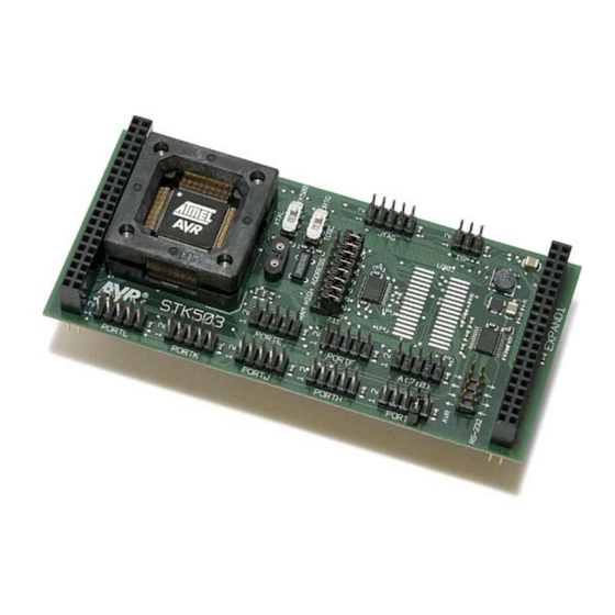
STK503 User Guide Introduction STK503 is a top module to the STK500 development board from Atmel Corporation. It adds support for 100-pin AVR microcontrollers (ATmega2560, ATmega1280 and ATmega640). STK503 includes connectors and hardware allowing full utilization of the features of these devices, while the Zero Insertion Force (ZIF) socket makes it easy to use TQFP packages for prototyping. -
Page 3: Known Issues
Known Issues January 2005: There are no known issues. -
Page 4: Getting Started
Getting Started In this chapter you will get an overview of all the features of the STK503. You will learn how to use the STK503 with STK500 and how to mount the AVR in the ZIF socket. Hardware overview The STK503 is a flexible tool to start developing and debugging applications for 100-pin AVRs as the ATmega2560. -
Page 5: Mounting The Stk503
SRAM. See the External Memory Interface chapter. RS-232 connector: The STK503 has an on-board RS-232 converter. In order to use it, you must connect the AVR to the AVR side of the connector, and the external RS-232 equipment (such as a PC) to the RS-232 side. See RS-232 Driver for more information. - Page 6 STK503. Make sure the STK500 power is switched off. Make sure that the STK503 is properly mounted on STK500. (See Mounting the STK503 for details.) Place the AVR in the ZIF socket. Pay attention to the pin 1 marking on the device and on the ZIF socket and PCB.
-
Page 7: Programming The Avr
Programming the AVR The AVR on STK503 can be programmed in four different ways: In-System Programming (ISP) High-Voltage Parallel Programming (HVPP) JTAG Programming Self Programming Self Programming in not described in this document. Please consult the specific AVR's datasheet. In-System Programming (ISP) In order to ISP program an AVR, it must have the ISP programming enable fuse set. -
Page 8: High-Voltage Parallel Programming (Hvpp)
HVPP requires the target voltage to be set to 5V. If you have any external hardware connected to STK500/STK503 that does not tolerate 5V, it must be disconnected before you HVPP program the AVR. Figure 4-2: HVPP programming the AVR To HVPP program the AVR on STK503, follow these steps: Turn off power on STK500. -
Page 9: Jtag Programming
Follow these steps to JTAG program the AVR: Turn off power on STK500. Connect the JTAGICE mkII probe to the JTAG connector on STK503. Remove the RESET jumper on STK500. Connect a serial cable or a USB cable beetween the JTAGICE mkII and your PC. -
Page 10: Stk503 Clock Sources
You select between these two sources with the OSCSEL jumper. This signal is available on STK503. The STK503 also has a socket for a crystal. This socket should be used instead of the one on STK500, at least for high-frequency crystals (>8MHz). -
Page 11: The Tosc Switch
(multiplexed data and address low byte), PORTC (address high byte), and PORTG[2:0] (RD, WR and ALE). SRAM footprint STK503 has a footprint where an SRAM chip can be mounted. The footprint takes 128Kx8 SOJ and TSOP packages. Figure 6-1: The SRAM footprint. The arrow shows pin 1. -
Page 12: Address Latch
The STK503's a latch is connected to the ALE signal. The latched low byte of the address is routed to the SRAM footprint, and is also accessible on the connector marked A[7:0]. -
Page 13: Rs-232 Driver
RS-232 Driver The STK503 has an RS-232 driver operating at target voltages from 1.8 to 5.5V with a maximum speed of 480kbps. There are two transmit and two receive pins. With the RS-232 port available on STK500, you have three channels available for your design. -
Page 14: Debugging With Jtagice Mkii
Debugging with JTAGICE mkII ATMEL's JTAGICE mkII can debug AVRs that supports the JTAG or the debugWire debugger interface. Connecting the JTAGICE Figure 8-1: Connecting the JTAGICE to STK503 Connect the JTAGICE probe to the JTAG connector as show in the figure above. -
Page 15: Troubleshooting Guide
STK503. See also Programming the AVR. ISP programming The ISP clock is to fast if Make sure the clock switch on STK503 is in the does not work the AVR is running at a low right position. In the Board page of the clock frequency. -
Page 16: Appendix
Appendix Port Connectors The STK503 has seven port connectors in addition to those available on STK500. These are PORTE, PORTF, PORTG, PORTH, PORTJ, PORTK and PORTL. The pinout of each connector is described below. Table A-1: STK503 port connectors pinout... -
Page 17: Schematic And Layout
Disclaimer: The information in this document is provided in connection with Atmel products. No license, express or implied, by estoppel or otherwise, to any intellectual property right is granted by this document or in connection with the sale of Atmel products. EXCEPT AS SET FORTH IN ATMEL’S TERMS AND CONDITIONS OF SALE LOCATED ON ATMEL’S WEB SITE, ATMEL ASSUMES NO LIABILITY...
Need help?
Do you have a question about the STK503 and is the answer not in the manual?
Questions and answers