Sony MZ-DH710 Service Manual
Portable md player
Hide thumbs
Also See for MZ-DH710:
- Operating instructions manual (6 pages) ,
- Specification sheet (2 pages) ,
- Operating instructions manual (79 pages)
Table of Contents
Advertisement
Quick Links
SERVICE MANUAL
Ver. 1.1 2010.10
US and foreign patents licensed from Dolby Laboratories.
• SonicStage and SonicStage logo are trademarks or registered trademarks
of Sony Corporation.
• MD Simple Burner, OpenMG, "Magic Gate", "MagicGate Memory
Stick", "Memory Stick", Hi-MD, Net MD, ATRAC, ATRAC3,
ATRAC3plus and their logos are trademarks of Sony Corporation.
• Microsoft, Windows, Windows NT and Windows Media are trademarks
or registered trademarks of Microsoft Corporation in the United States
and /or other countries.
• IBM and PC/AT are registered trademarks of International Business
Machines Corporation.
• Macintosh is a trademark of Apple Computer, Inc. in the United States
and/or other countries.
• Pentium is a trademark or registered trademark of Intel Corporation.
• All other trademarks and registered trademarks are trademarks or
registered trademarks of their respective holders.
• ™ and ® marks are omitted in this manual.
• CD and music-related data from Gracenote, Inc., copyright © 2000-2004
®
Gracenote. Gracenote CDDB
Client Software, copyright 2000-2004
Gracenote. This product and service may practice one or more of the
following U.S. Patents: #5,987,525; #6,061,680; #6,154,773, #6,161,132,
#6,230,192, #6,230,207, #6,240,459, #6,330,593, and other patents issued
or pending. Services supplied and/or device manufactured under license
for following Open Globe, Inc. United States Patent 6,304,523. Gracenote
is a registered trademarks of Gracenote. The Gracenote logo and logotype,
and the "Powered by Gracenote" logo are trademarks of Gracenote.
Program © 2001, 2002, 2003, 2004, 2005 Sony Corporation
Documentation © 2005 Sony Corporation
9-879-660-02
Sony Corporation
2010J00-1
Published by Sony Techno Create Corporation
© 2010.10
MZ-DH710
Model Name Using Similar Mechanism
MD Mechanism Type
Optical Pick-up Name
SPECIFICATIONS
Audio playing system
MiniDisc digital audio system
Laser diode properties
Material: GaAlAs
Wavelength: λ = 790 nm
Emission duration: continuous
Laser output: less than 44.6 µW
(This output is the value measured at a distance
PORTABLE MD PLAYER
US Model
Canadian Model
NEW
MT-MZNH900-181
ABX-U
– Continued on next page –
Advertisement
Table of Contents

Related Manuals for Sony MZ-DH710


Summary of Contents for Sony MZ-DH710
- Page 1 • MD Simple Burner, OpenMG, “Magic Gate”, “MagicGate Memory Stick”, “Memory Stick”, Hi-MD, Net MD, ATRAC, ATRAC3, SPECIFICATIONS ATRAC3plus and their logos are trademarks of Sony Corporation. • Microsoft, Windows, Windows NT and Windows Media are trademarks or registered trademarks of Microsoft Corporation in the United States...
- Page 2 16.0 19.0 18.5 standard disc When using a new Sony LR6 (size AA) alkaline dry battery (produced in Japan) Measured in accordance with the JEITA (Japan Electronics and Information Technology Industries Association) standard. Tracks transferred at 128 kbps. When playing continuously in MD mode (Unit: approx.
-
Page 3: Table Of Contents
LES DIAGRAMMES SCHÉMATIQUES ET LA LISTE DES PIÈCES SONT CRITIQUES POUR LA SÉCURITÉ DE FONCTIONNEMENT. NE REMPLACER CES COM- POSANTS QUE PAR DES PIÈCES SONY DONT LES NUMÉROS SONT DONNÉS DANS CE MANUEL OU DANS LES SUPPLÉMENTS PUBLIÉS PAR SONY. -
Page 4: Servicing Notes
MZ-DH710 SECTION 1 SERVICING NOTES OPERATION CHECK WHEN THE MAIN BOARD IS NOTES ON HANDLING THE OPTICAL PICK-UP REMOVED BLOCK OR BASE UNIT In making an operation check with the MAIN board removed from The laser diode in the optical pick-up block may suffer electrostatic... -
Page 5: General
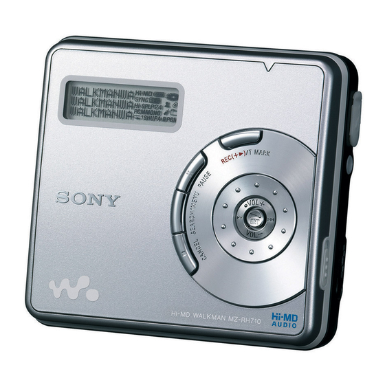
MZ-DH710 SECTION 2 This section is extracted from instruction manual. GENERAL Looking at controls The player A OPEN switch H 5-way control key B Display window C DOWNLOAD button This button allows you to record music tracks from an audio CD in the... -
Page 6: Disassembly
MZ-DH710 SECTION 3 DISASSEMBLY • This set can be disassembled in the order shown below. 3-1. DISASSEMBLY FLOW Note 1: The process described in can be performed in any order. Note 2: Without completing the process described in , the next process can not be performed. -
Page 7: Case (Lower) Section
MZ-DH710 3-2. CASE (LOWER) SECTION 1 two screws (M1.4) 1 two screws (M1.4) 2 Remove the case (lower) section in the direction of the arrow. 3-3. MAIN BOARD 3 flexible board (CN471) 6 flexible board (CN501) 7 MAIN board 1 Remove two solders. -
Page 8: Case (Upper) Section
MZ-DH710 3-4. CASE (UPPER) SECTION 7 case (upper) section 4 two step screws 6 boss 1 flexible board (CN471) 3 torsion spring (pop up L) 2 Open the case (upper) section. 3-5. MECHANISM DECK SECTION (MT-MZNH900-181), MD STANDARD PIN 1 two step screws (MD) -
Page 9: Set Chassis Assy
MZ-DH710 3-6. SET CHASSIS ASSY 5 two screws 1 torsion coil spring (R) 2 extension spring (R) 7 set chassis assy 6 battery case 3 compression coil spring (limitter) 4 open slider 3-7. GEAR (BSA), GEAR (SB) 1 self tap screw 2 thrust retainer spring 3 washer (0.8-2.5) -
Page 10: Op Service Assy
MZ-DH710 3-8. OP SERVICE ASSY 1 Lead screw block assy is turned and it removes from OP service assy. 2 OP service assy 3-9. DC MOTOR SSM18D/C-NP (SPINDLE) (M701), DC MOTOR (SLED) (M702), DC MOTOR UNIT (OVER WRITE HEAD UP/DOWN) (M703) 3 two screws (M1.4) -
Page 11: Holder Assy
MZ-DH710 3-10. HOLDER ASSY 4 Remove the holder assy to the direction of the arrow A . 2 boss 3 Open the holder assy. 1 boss 3-11. POSITION OF FERRITE CORE -EARPHONES- A cable is rolled once. clamp filter (ferrite core) (Part No. -
Page 12: Test Mode
MZ-DH710 SECTION 4 TEST MODE OUTLINE 2. CONFIGURATION OF THE TEST MODE Operation in the test mode is performed with the set. A key having Flow of the test mode: no particular description in the text, indicates a set key. Also, For the LCD display, the LCD on the set is shown. - Page 13 MZ-DH710 3. MANUAL MODE This is mode to adjust or check the operation of the set by function. • Item Title Display Set LCD display Operation of The Manual Mode 1. Enter the test mode (Display Check mode). XXXX item number 2.
- Page 14 MZ-DH710 4. OVERALL ADJUSTMENT MODE 4-2. Error Message in The Overall Adjustment Mode 4-1. Operation of The Overall Adjustment Mode In the Overall Adjustment mode, if an error occurred, it displays as 1. Enter the test mode (Display Check mode).
- Page 15 MZ-DH710 Flow of Self-diagnosis Result Display mode operation: 5-3. Clear The Total Recording Time After replacing the optical pick-up, clear the total recording time. 1. Enter the test mode (Display Check mode). The first error **** 2. Press the key to activate the Self-Diagnosis Result Display >...
-
Page 16: Electrical Adjustments
MZ-DH710 SECTION 5 ELECTRICAL ADJUSTMENTS 1. PRECAUTIONS FOR ADJUSTMENT 5. Measure the ambient temperature. 1. Adjustment must be done in the test mode only. After adjusting, 6. Adjust with [VOL+]/[VOL--] keys so that the adjusted value release the test mode. A key having no particular description (hexadecimal value) becomes the ambient temperature. - Page 17 MZ-DH710 3-3-3. VBsAdj adjustments ItemNo. Display Specification value Measuring point Procedure: 2211 211 VC1 ** 2.05V + 0.02V CL8027 1. In the “3-3-2. PwrAdj Adjustments” completed status, display 2.25V ± 0.01V 2212 212 VC1H N ** CL8027 as follows. 2213 213 VC2 ** 1.20V + 0.01V...
- Page 18 MZ-DH710 Ver. 1.1 7. Select the item number 2244, and turn off the power supply of *1) If the “Pr_nominal” value is indicated, use the “Pr_nominal” value and not used “Por” value. battery terminal. *2) If the “Pw_nominal” value is indicated, use the “Pw_nominal” value 8.
- Page 19 MZ-DH710 3-5-3. Other setting 3-6. Servo Overall Adjustment Procedure: Note1: Be sure to adjustment so that the set is horizontal and the LCD is upside. Unless performed in that state, it is not adjusted correctly. 1. Enter the test mode (Display Check mode).
- Page 20 MZ-DH710 MEMO...
-
Page 21: Diagrams
MZ-DH710 SECTION 6 DIAGRAMS 6-1. BLOCK DIAGRAM – MD SERVO Section – OVER WRITE HEAD DRIVE IC601 (1/2) HR601 (Page 22) OVER WRITE OVER 69 HBB HEAD DRIVE WRITE 78 HB Q601, 602 HEAD 70 HBA EFM_CLK LATCH M703 OUTA... -
Page 22: Block Diagram - Power Supply Section
MZ-DH710 6-2. BLOCK DIAGRAM – POWER SUPPLY Section – (Page 21) SDO0 DATA SDO0 SCK0 SCK0 (Page 21) VRMC RMC KEY (Page 21) XWK3 XWK4 WAKE UP SWITCH 5 XWK1 Q902 XWK2 S892 S892 HALF_LOCK_SW/ HALF YUZU_SLEEP SLEEP OPEN_SW LOCK... - Page 23 MZ-DH710 • Note For Printed Wiring Boards and Schematic Diagrams • Waveforms Note on Printed Wiring Board: Note on Schematic Diagram: IC501 8 (RFO) • X : parts extracted from the component side. • All capacitors are in µF unless otherwise noted. (p: pF) •...
-
Page 24: Printed Wiring Board - Main Section (1/2)
MZ-DH710 6-3. PRINTED WIRING BOARD – MAIN Section (1/2) – : Uses unleaded solder. • Semiconductor Location Ref. No. Location D151 D440 S894-1 D457 S894 PROTECT D458 DETECT D605 S894-2 D606 Hi-MD PROTECT D607 DETECT D608 D614 D615 D616 CN451... -
Page 25: Printed Wiring Board - Main Section (2/2)
MZ-DH710 6-4. PRINTED WIRING BOARDS – MAIN Section (2/2) – : Uses unleaded solder. • Semiconductor Location MAIN BOARD Ref. No. Location (CONDUCTOR SIDE) D251 D352 D471 D601 S892 M702 D602 (HALF LOCK) (SLED) D603 D604 D609 M703 D610 OVER WRITE... -
Page 26: Schematic Diagram - Main Section (1/8)
MZ-DH710 6-5. SCHEMATIC DIAGRAM – MAIN Section (1/8) – • See page 34 for IC Block Diagram. (1/8) XRST_MTR_DRV XRST_MTR_DRV SLD_CON_W C714 SLD_CON_W SLD_CON_V SLD_CON_V SLD_CON_U SLD_CON_U SLD_PWM L701 L702 SLD_PWM SLD_MON_U SLD_MON_U SLD_MON_V SLD_MON_V SLD_MON_W SLD_MON_W SLD_CON_W R706 2.2k R707 2.2k... -
Page 27: Schematic Diagram - Main Section (2/8)
MZ-DH710 • See page 34 for IC Block Diagrams. 6-6. SCHEMATIC DIAGRAM – MAIN Section (2/8) – (2/8) XCS_REC_DRV SUSPEND C673 SUSPEND REG_DACVREFH USB_HOLD USB_HOLD RECP RECP C668 EFM_CLK D610 EFM_CLK MA2Z748001S0 C669 C643 VOLTAGE DETECT XCS_REC_DRV IC606 XCS_REC_DRV +1.2V REGULATOR... -
Page 28: Schematic Diagram - Main Section (3/8)
MZ-DH710 • See page 23 for Waveforms. • See page 34 for IC Block Diagram. 6-7. SCHEMATIC DIAGRAM – MAIN Section (3/8) – (Page 26) (3/8) C553 C554 6.3V C523 C524 C530 0.01 (Page 27) R505 L503 10µH C519 XLDON... -
Page 29: Schematic Diagram - Main Section (4/8)
MZ-DH710 6-8. SCHEMATIC DIAGRAM – MAIN Section (4/8) – (4/8) (Page 33) (Page 27) Q451 RTQ035P02TR MINUS_MON GND_SW VBUS_MON (Page 33) C453 0.047 Q451,452 VOLTAGE LIMITER R463 R464 R467 100k Q452 XP4601-TXE CL431 W403 DRY BATTERY C423 C424 SIZE"AA" C452... -
Page 30: Schematic Diagram - Main Section (5/8)
MZ-DH710 • See page 34 for IC Block Diagram. 6-9. SCHEMATIC DIAGRAM – MAIN Section (5/8) – (Page 27) (5/8) (Page 28) L903 10µH C927 C915 100p L9001 6.3V 10µH C922 C923 C958 C928 C929 R954 R955 100p 1000p 470k 2.2k... -
Page 31: Schematic Diagram - Main Section (6/8)
MZ-DH710 • See page 34 for IC Block Diagram. 6-10. SCHEMATIC DIAGRAM – MAIN Section (6/8) – (Page 27) (6/8) C354 R352 220k Q353 SI1410EDH-T1 R356 100k Q351 2SC4738F-Y/GR (TPL3) REFERENCE AOUTL AOUTL VOLTAGE SWITCH AOUTR C351 R353 AOUTR XHP_STBY... -
Page 32: Schematic Diagram - Main Section (7/8)
MZ-DH710 • See page 34 for IC Block Diagram. 6-11. SCHEMATIC DIAGRAM – MAIN Section (7/8) – (7/8) R478 4.7k R476 R477 4.7k 4.7k CN471 R486 DVDD R471 JOG_B XRST2 JOG_B R472 JOG_A JOG_A SET_KEY_2 SET_KEY_2 SET_KEY_1 SET_KEY_1 R473 REC_KEY... -
Page 33: Schematic Diagram - Main Section (8/8)
MZ-DH710 • See page 23 for Waveforms. • See page 37 for IC Pin Function Description. 6-12. SCHEMATIC DIAGRAM – MAIN Section (8/8) – (8/8) C861 POEN_CLOSE_SW WK_DET (Page 32) R876 R868 Q803 2SC4738F-Y/GR (TPL3) R880 R842 R861 R813 WAKE UP... - Page 34 MZ-DH710 • IC Block Diagrams IC601 SC901585VAR2 IC352 TA2131FLG (EL) BEEP V REF VREF CHARGE PUMP LPF1 NC A12 MT TC 56 LATCH VCC1 EFM BOTTOM 55 XWKO LVDT WAKE PRE DRIVER BST NF1 HOLD OUT HOLD CONTROL BST1 VBUS...
- Page 35 MZ-DH710 IC701 BD6607KN 62 61 48 WI2 STANDBY DECODER DECODER PRE DRIVE PRE DRIVE PGNDW1 47 PGNDW2 46 WO2 45 ST2 VMVW1 44 VMVW2 43 VO2 42 VO2 PGNDUV1 41 PGNDUV2 40 UO2 39 UO2 VMU1 38 VMU2 VMR1 37 VMR2...
- Page 36 MZ-DH710 IC901 SC901584EPR2 36 35 RESET 2 SERIAL RST2 PASS POWER STEP REGULATOR 3 SWITCH 2 UP-DOWN REGC2 DRIVER RST2 MUTING REG2G VREF REF2 SERIAL BUFFER REGO2 PASS REGULATOR 2 REGI2 32 DTC2 REGC1 VREF RST1 SERIAL REF2 REGO1 PASS...
- Page 37 MZ-DH710 • IC Pin Function Description IC801 CXD2681-225GG (SYSTEM CONTROLLER, DIGITAL SIGNAL PROCESSOR) Pin No. Pin Name Description DVDD1_0 — Power supply terminal DVSS1_0 — Ground terminal DVDD1_1 — Power supply terminal DVSS1_1 — Ground terminal DVDD1_2 — Power supply terminal DVSS1_2 —...
- Page 38 MZ-DH710 Pin No. Pin Name Description DAVDD — Power supply terminal (for D/A converter) DVDD25LPF — Power supply terminal (for D/A converter) DAVSS — Ground terminal (for D/A converter) OSCVDD — Power supply terminal (for 22 MHz OSC) USBOSCVDD —...
- Page 39 MZ-DH710 Pin No. Pin Name Description Phase comparison output terminal for the playback EFM system master PLL FILI Filter input terminal for the playback EFM system master PLL FILO Filter output terminal for the playback EFM system master PLL CLTV...
- Page 40 MZ-DH710 Pin No. Pin Name Description VREFL Reference voltage terminal connected to the capacitor (for the built-in D/A converter L-CH) AOUTL Built-in D/A converter L-CH signal output AOUTR Built-in D/A converter R-CH signal output VREFR Reference voltage terminal connected to the capacitor (for the built-in D/A converter R-CH)
- Page 41 MZ-DH710 Pin No. Pin Name Description Serial data input from the EEPROM Serial data output to the EEPROM SCK0 Serial clock output to the EEPROM XGUM_ON Rechargeable battery detection signal terminal Not used BEEP Beep sound control signal output to the headphone amplifier...
- Page 42 MZ-DH710 Pin No. Pin Name Description XRST_MTR Reset signal output to the motor driver _DRV XCS_NV Chip select signal output to the EEPROM CHG_PWM Charge current or voltage control signal output terminal Not used IAMP_CAL Offset signal output of current sense amplifier Not used —...
- Page 43 MZ-DH710 Pin No. Pin Name Description SCS4 Chip select signal output for ATRAC3 plus encoder communication Not used HI_Z_SLD Standby signal output terminal for the sled motor HI_Z_SPDL Standby signal output terminal for the spindle motor 291 to SET_CODE0 to...
-
Page 44: Exploded Views
MZ-DH710 SECTION 7 EXPLODED VIEWS NOTE: • Items marked “*” are not stocked since they • -XX and -X mean standardized parts, so they The components identified by mark 0 or dotted line with mark 0 are may have some difference from the original are seldom required for routine service. -
Page 45: Case (Upper) Section
MZ-DH710 7-2. CASE (UPPER) SECTION LCD101 SWITCH board Ref. No. Part No. Description Remark Ref. No. Part No. Description Remark 3-249-687-91 KNOB (HOLD) 2-541-972-01 BUTTON (CONTROL) X-2055-992-1 CASE UPPER ASSY, SVX (DOWNLOAD. X. SEARCH/MENU. CANCEL) 3-266-189-01 LOCKER, OPEN 2-541-969-01 HOLDER (LCD) -
Page 46: Chassis Section
MZ-DH710 7-3. CHASSIS SECTION mechanism deck section MAIN board Ref. No. Part No. Description Remark Ref. No. Part No. Description Remark 3-266-202-01 SPRING (LIMITTER), COMPRESSION COIL 3-238-876-04 SCREW (M1.4), TOOTHED LOCK 3-266-197-01 OPEN SLIDER 3-266-204-01 TERMINAL (+), BATTERY 3-266-196-01 CASE, BATTERY... -
Page 47: Mechanism Deck Section (Mt-Mznh900-181)
MZ-DH710 7-4. MECHANISM DECK SECTION (MT-MZNH900-181) not supplied HR601 (over write head) M702 M703 (including HR601 (over write head) ) M701 Ref. No. Part No. Description Remark Ref. No. Part No. Description Remark 3-338-645-31 WASHER (0.8-2.5) X-2023-272-1 SERVICE ASSY, LEAD SCREW... -
Page 48: Electrical Parts List
MZ-DH710 SECTION 8 MAIN ELECTRICAL PARTS LIST NOTE: • Items marked “*” are not stocked since they • Due to standardization, replacements in the The components identified by mark 0 or dotted line with mark 0 are parts list may be different from the parts are seldom required for routine service. - Page 49 MZ-DH710 MAIN Ref. No. Part No. Description Remark Ref. No. Part No. Description Remark C567 1-135-210-11 TANTALUM CHIP 4.7uF C570 1-165-847-91 TANTALUM CHIP 4.7uF C708 1-107-819-11 CERAMIC CHIP 0.022uF C573 1-164-937-11 CERAMIC CHIP 0.001uF C709 1-164-943-11 CERAMIC CHIP 0.01uF C710 1-107-819-11 CERAMIC CHIP 0.022uF...
- Page 50 MZ-DH710 MAIN Ref. No. Part No. Description Remark Ref. No. Part No. Description Remark C918 1-165-176-11 CERAMIC CHIP 0.047uF D803 6-500-813-01 DIODE MA2SD32008S0 C919 1-164-227-11 CERAMIC CHIP 0.022uF D902 8-719-072-27 DIODE MA2Z748001S0 C920 1-125-777-11 CERAMIC CHIP 0.1uF D904 8-719-072-27 DIODE MA2Z748001S0...
- Page 51 MZ-DH710 MAIN Ref. No. Part No. Description Remark Ref. No. Part No. Description Remark L603 1-414-398-11 INDUCTOR 10uH R152 1-218-957-11 RES-CHIP 2.2K 1/16W L605 1-416-669-11 INDUCTOR 22uH R153 1-218-965-11 RES-CHIP 1/16W R154 1-218-965-11 RES-CHIP 1/16W L606 1-400-626-11 INDUCTOR 10uH R155...
- Page 52 MZ-DH710 MAIN Ref. No. Part No. Description Remark Ref. No. Part No. Description Remark R512 1-218-990-11 SHORT CHIP R673 1-218-990-11 SHORT CHIP R675 1-220-804-11 RES-CHIP 2.2M 1/16W R513 1-218-965-11 RES-CHIP 1/16W R677 1-216-864-11 SHORT CHIP R514 1-218-973-11 RES-CHIP 1/16W R679...
- Page 53 MZ-DH710 MAIN SWITCH Ref. No. Part No. Description Remark Ref. No. Part No. Description Remark R860 1-218-929-11 RES-CHIP 1/16W S894 1-786-703-21 SWITCH, PUSH (2 KEY) (PROTECT DETECT, Hi-MD PROTECT DETECT) R861 1-218-990-11 SHORT CHIP R862 1-218-989-11 RES-CHIP 1/16W < VIBRATOR >...
- Page 54 MZ-DH710 REVISION HISTORY Clicking the version allows you to jump to the revised page. Also, clicking the version at the top of the revised page allows you to jump to the next revised page. Ver. Date Description of Revision 2005.04 2010.10...
Need help?
Do you have a question about the MZ-DH710 and is the answer not in the manual?
Questions and answers