Table of Contents
Advertisement
SERVICE MANUAL
Ver. 1.0 2018.02
• SA-Z9R other than the AUS model is an optional rear
speaker for exclusive HT-Z9F/ZF9.
• SA-Z9R of AUS model is a package rear speaker for
HT-Z9RF.
• Except AUS model
All of the units included in the right and left rear speak-
ers (SA-LZ9R/RZ9R) and the HT-Z9F (SA-Z9F/SA-
WZ9F/Remote control) or HT-ZF9 (SA-ZF9/SA-WZF9/
Remote control) are required to confi rming operation of
this unit. Check in advance that you have all of the units.
• AUS model
All of the units included in the right and left rear speakers
(SA-LZ9R/RZ9R) and the HT-Z9RF (SA-Z9F/SA-WZ9F/
Remote control) are required to confi rming operation of
this unit. Check in advance that you have all of the units.
COMPONENT MODEL NAME (SA-Z9R)
Rear speaker L-ch
Rear speaker R-ch
Amplifier section
U.S. models:
POWER OUTPUT AND TOTAL HARMONIC DISTORTION:
(FTC)
With 4 ohms loads, both channels driven, from 200 -
20,000 Hz; rated 20 W per channel minimum RMS power,
with no more than 1% total harmonic distortion from
POWER OUTPUT (reference)
50 W (per channel at 4 ohms, 1 kHz)
Except US model:
POWER OUTPUT (rated)
30 W + 30 W (at 4 ohms, 1 kHz, 1% THD)
POWER OUTPUT (reference)
50 W (per channel at 4 ohms, 1 kHz)
Speaker system
Full range speaker system, Acoustic suspension
Speaker
46 mm (1 13/16 in) cone type, Full range speaker
Power requirements
120 V AC, 60 Hz (US, CND)
220 V - 240 V AC, 50 Hz/60 Hz (AEP, UK, AUS)
Power consumption
On: 11 W
Standby mode: 1 W or less
Turned off: 0.5 W or less
Dimensions (w/h/d) (approx.)
100 mm × 155 mm × 100 mm (4 in × 6 1/8 in × 4 in)
(projecting parts not included)
Mass (approx.)
1.0 kg (2lb 3 3/8 oz)
9-896-494-01
2018B33-1
Sony Video & Sound Products Inc.
©
2018.02
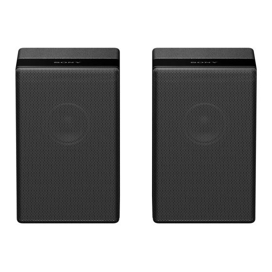
Photo: SA-LZ9R
SA-LZ9R
SA-RZ9R
SPECIFICATIONS
Wireless transmitter/receiver section
Communication system
Wireless Sound Specification Version 4.0
Frequency band
5 GHz
Modulation method
OFDM
Radio Frequency Bands and Maximum Output
Power
Frequency band
5150 - 5250 MHz
5250 - 5350 MHz
5470 - 5600 MHz
5650 - 5725 MHz
5725 - 5850 MHz
Included items
• Rear speaker R (1), Rear speaker L (1)
• Operating Instructions (1)
SA-Z9R
(L-ch)
Photo: SA-RZ9R
(R-ch)
On copyrights
This product contains software that is subject to the
GNU General Public License ("GPL") or GNU Lesser
General Public License ("LGPL"). These establish that
customers have the right to acquire, modify, and
redistribute the source code of said software in
accordance with the terms of the GPL or the LGPL.
For details of the GPL, LGPL and other software
licenses, please refer to [Software License
Information] under
Maximum output power
- [System Settings] on the product.
< 18 dBm
The source code for the software used in this product
< 18 dBm
is subject to the GPL and LGPL, and is available on
< 18 dBm
the Web. To download, please access the following:
< 18 dBm
URL:
< 13.98 dBm
http://oss.sony.net/Products/Linux
Please note that Sony cannot answer or respond to
any inquiries regarding the content of this source
code.
All other trademarks are trademarks of their
respective owners.
ACTIVE REAR SPEAKER
SA-LZ9R/RZ9R
US Model
Canadian Model
AEP Model
UK Model
Australian Model
[Setup] - [Advanced Settings]
Advertisement
Table of Contents


Need help?
Do you have a question about the SA-Z9R and is the answer not in the manual?
Questions and answers