Advertisement
Quick Links
AN107
AN107
CMT2210A Schematic and PCB Layout Design Guideline
1. Introduction
The purpose of this document is to provide the guidelines to design a low power consumption, low BOM and high
sensitivity CMT2210A Receiver.
2. CMT2210A Schematics Guidelines
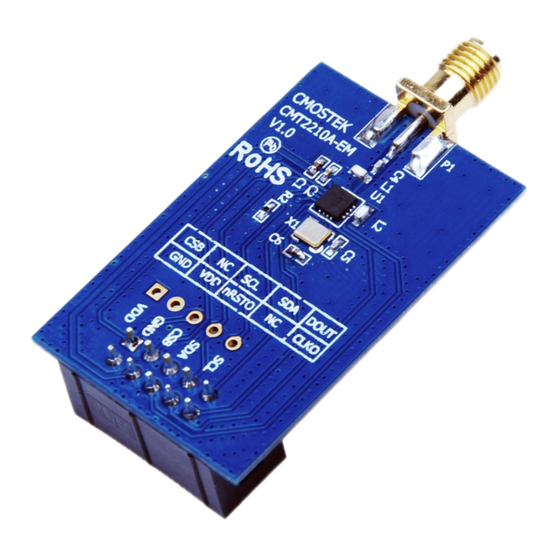
The CMT2210A is an ultra low power, high performance, low-cost OOK stand-alone RF receiver for various 300 to
TM
480 MHz wireless applications. The chip is part of the CMOSTEK NextGenRF
family, which includes a complete
line of transmitters, receivers and transceivers. To give the CMT2210A schematic design guidelines, an example of
315/433.92 MHz application is given below.
2.1 CMT2210A Evaluation Module Schematic
Only a few external components are required for the CMT2210A. Further optimizations can be done by removing
the connections of the optional pins.
Figure 1. CMT2210A-EM Schematic
Copyright © By CMOSTEK
www.hoperf.com
Rev 1.0 | Page 1/10
Advertisement

Related Manuals for CMOSTEK CMT2210A


Summary of Contents for CMOSTEK CMT2210A
- Page 1 CMT2210A Receiver. 2. CMT2210A Schematics Guidelines The CMT2210A is an ultra low power, high performance, low-cost OOK stand-alone RF receiver for various 300 to 480 MHz wireless applications. The chip is part of the CMOSTEK NextGenRF family, which includes a complete line of transmitters, receivers and transceivers.
- Page 2 CLKO pin to drive the external device. The nRSTO and CLKO should be left un-connected if they are not used. 10. Pin descriptions of the CMT2210A, and the BOM for CMT2210A application are shown in Table 1 and Table 2. www.hoperf.com...
- Page 3 Active-low power-on-reset output to reset an external MCU VCOP VCO tank, connected to an external inductor VCON 13, 15 Ground RFIN RF input Power supply input Table 2. BOM of CMT2210A-EM Application Value Manufacturer Designator Descriptions Unit 315 MHz 433.92 MHz CMT2210A 300-480MHz OOK receiver CMOSTEK ±5%,0603 multi-layer chip inductor...
- Page 4 The following PCB layout design guidelines take the CMT2210A-EM as an example. CMT2210A-EM is a 2-layer PCB using FR4 PCB material. The thickness of the PCB is 0.8 mm; the thickness for the copper is 1 ounce (0.0356mm); the separation between ground pour copper and traces/pads is 0.3 mm; the dielectric constant (Er) for the FR4 material is 4.4.
- Page 5 The input of the LNA can be modeled as a shunt resistor R (2.8 pF). A 0.2-mm width transmission line between the L1 and the CMT2210A is used. The width of the transmission line is 1 mm between L1 and the SMA connector which is of 50 Ω impedance.
- Page 6 AN107 Figure 4.Power Supply Decoupling Layout 3.1.3 XTAL Place the crystal as close as possible to the XTAL pin and keep the routing as short as possible in order to reduce any frequency offsets that may occur. Avoid routing digital signals with sharp edges close to XIN PCB track or underneath the crystal X1 pad, as this may shift the crystal DC operating point and result in duty-cycle variation.
- Page 7 To minimize the radiation from the VCO circuit and maintain the high Q factor of the VCO tank, L2 should be placed as close as possible to the CMT2210A. The VCO tank is surrounded by a solid ground plane.
- Page 8 AN107 3.1.6 Grounding Use as much continuous ground plane metallization as possible. Place a series of ground vias along the PCB edges if possible. The maximum distance between the vias should be less than λ/10. This is required to reduce the PCB radiation at higher harmonics caused by the fringing field of routing edges.
-
Page 9: Document Change List
AN107 4. Document Change List Table 3. Document Change List Rev. No Chapter Description of Changes Date Initial released version 2014-06-14 2014-06-30 www.hoperf.com Rev 1.0 | Page 9/10... -
Page 10: Contact Information
Copyright. CMOSTEK Microelectronics Co., Ltd. All rights are reserved. The information furnished by CMOSTEK is believed to be accurate and reliable. However, no responsibility is assumed for inaccuracies and specifications within this document are subject to change without notice. The material contained herein is the exclusive property of CMOSTEK and shall not be distributed, reproduced, or disclosed in whole or in part without prior written permission of CMOSTEK.
Need help?
Do you have a question about the CMT2210A and is the answer not in the manual?
Questions and answers