Table of Contents
Advertisement
PROPRIETARY NOTICE
All rights reserved by Janz Tec AG.
No parts of this technical manual may be modified, copied or reproduced
in any form or by any means for commercial use without the prior written
permission of Janz Tec AG, Germany.
All instructions, information and specification contained in this manual
are for reference only and remain subject to change without
announcement.
emPC-CX+
embedded computer system
(System Reference Manual)
Version 1.2
refers to product revision no.
V -
Advertisement
Table of Contents

Related Manuals for Janz Tec emPC-CX+


Summary of Contents for Janz Tec emPC-CX+
- Page 1 PROPRIETARY NOTICE All rights reserved by Janz Tec AG. No parts of this technical manual may be modified, copied or reproduced in any form or by any means for commercial use without the prior written permission of Janz Tec AG, Germany.
- Page 2 Title: emPC-CX platforms systems reference File: j:\as\entwicklung\projekte\hw\empc\empc_+\doc\manual\manual_empc- cxplus_platforms_system_reference.doc Pattern: c:\users\as\appdata\roaming\microsoft\templates\normal.dotm Created: 24.09.2012 Last Update: Stefan Althöfer, 02.06.2015 © Janz Tec AG 2014 Im Dörener Feld 8 PO Box 1906 D-33 049 Paderborn, Germany Tel.: +49-5251-1550-0 FAX: +49-5251-1550-90 email: support@janztec.com Internet:...
-
Page 3: Table Of Contents
I2C Address ........................26 3.1.2 I2C Registers ........................26 3.1.3 Command Codes ......................31 FAN Controller ........................32 3.2.1 I2C Communication ......................32 3.2.2 I2C Address ........................33 3.2.3 Registers ........................33 3.2.4 Command Codes ......................36 3.2.5 Configuration .........................37 Appendices References .........................38 Rev. 1.2 © Janz Tec AG... - Page 4 (System Reference Manual) Personality Board Connector .....................39 Product History........................41 Manual History ........................42 © Janz Tec AG Rev. 1.2...
- Page 5 Table 9: Local address spaces .......................16 Table 10: Control registers ........................17 Table 11: NVRAM address (128KByte NVRAM)..................21 Table 12: Digital IO registers ........................22 Table 13: Personality board connector pin assignment .................39 Table 14: Personality board connector signal description ..............40 Rev. 1.2 © Janz Tec AG...
- Page 6 It describes the features and architecture of the CX series. After that it discusses some topics about programming for these products. For a description of the emPC-CX+ and emPC-CX+ refer to the respective hardware manuals; the Janz Tec AG homepage gives information about it. Conventions DANGER indicates that death or severe personal injury will result if proper precautions are not taken.
- Page 7 Media Dependent Interface Crossover MDIX Medium Independent Interface NVRAM Non volatile RAM. Storage is ensured by a battery or flash memory backup Printed Circuit Board PHYsical Layer in ISO/OSI-Standard Pulse Width Modulation Universal Serial Bus Rev. 1.2 © Janz Tec AG...
-
Page 9: Introduction
status LEDs for power-on and HDD activity internal LVDS port for use in combination with emVIEW displays internal serial port for the touch screen (emVIEW display only) internal 2x SATA connector for SATA 2,5’’ HDD Rev. 1.2 © Janz Tec AG... -
Page 10: Functional Overview
2xPCIe PCIe Riser Card Connector Figure 1: emPC-CX+ block diagram A variety of customization options are available: PCIe slots with various riser cards PCIe Mini Card I/O Interfaces with personality board © Janz Tec AG Rev. 1.2... -
Page 11: Front Connectors
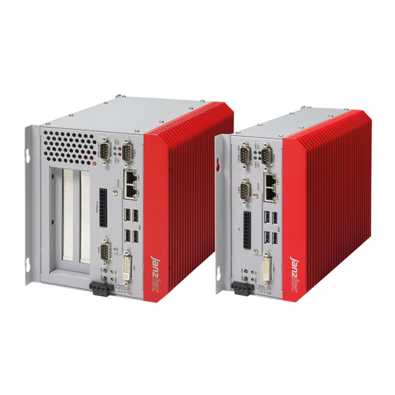
(System Reference Manual) Introduction 1 - 9 Front Connectors Headers defined by personality module CFast DVI-I Serial 1 4 x USB LAN-2 LAN-1 Figure 2: emPC-CX+ carrier module front connectors Rev. 1.2 © Janz Tec AG... -
Page 12: Personality Board
2 x CAN (isolated) BO-EPC-CPPS0 1 x CAN (isolated), 1 x RS232, digital IO BO-EPC-CPPS1 1 x CAN (isolated), 1 x RS232 BO-EPC-CPPU0 4 x RS232, USB based (suitable for CX+ Lite) Table 1: Available Personality Board © Janz Tec AG Rev. 1.2... -
Page 13: Safety Instructions
Danger of explosion when replacing with wrong type of battery. Replace only with battery of the same or equivalent type. Ambient and Environmental Conditions CAUTION Do not operate the boards beyond the specified ambient conditions. DANGER Do not operate the boards in potentially explosive atmosphere. Rev. 1.2 © Janz Tec AG... -
Page 14: Hardware Details
(some ATOM base low power modules do not) DVI digital signals provided by the COM Express DDI1 interface. This feature is only available if this interface can be configured for DVI/HDMI mode (sometime called TMDS). © Janz Tec AG Rev. 1.2... -
Page 15: Ethernet
The emPC-CX+ uses the COM Express defined SATA interfaces to connect mass storage. COM Express Usage SATA channel SATA0 CFast socket SATA1 Internal 7pin SATA header SATA2 Internal 7 pin SATA header SATA3 unused Table 4: COM Express SATA usage Rev. 1.2 © Janz Tec AG... -
Page 16: Lvds
Connected to COM Express LVDS_VDD_EN signal. BIASON Output Controls contrast voltage panel. Connected to COM Express LVDS_BKLT_CTRL signal. LDDETECT Output LVDS mapping selection. Driven to +3V3 to indicate that the LVDS signals © Janz Tec AG Rev. 1.2... -
Page 17: Display Touch- And Power-Connector
Input power supply fed through for display interface logic. Display and Touch power use this power supply to generate required power supplies (e.g. +12V). USB+/USB- Internal USB interface for touch (COM Express USB4) Rev. 1.2 © Janz Tec AG... -
Page 18: Fpga Expansion Subsystem
(System Reference Manual) FPGA expansion subsystem 2 - 16 FPGA expansion subsystem The PCIe interface for special Janz Tec Features is implemented by a FPGA and is identified by a set of IDs in PCIe configuration space as listed below: Purpose... -
Page 19: Control Registers
Interrupt status info. Each defined bit in this register reflects the status of the INT# pin of the corresponding CAN. A zero will be read when an interrupt is pending. If a CAN interrupt request line is disabled, then the corresponding bit is Rev. 1.2 © Janz Tec AG... -
Page 20: Function Reset
INT_STAT register and it will not cause interrupts. Reserved Reserved bit positions must be written as zero. 2.1.4 Internal I C bus The control register for the onboard I C interface provides bit-bang style I2C implementation. © Janz Tec AG Rev. 1.2... -
Page 21: Can Interface
Write 1 to turn red LED on, write 0 to disable. LEDG Write 1 to turn green LED on, write 0 to disable. Reserved Reserved positions should be written as zero for compatibility with future products. Rev. 1.2 © Janz Tec AG... -
Page 22: Serial Port Interface
LPC based legacy serial ports (IO address) can be implemented in FPGA if legacy ports are required for software compatibility. BIOS support for such ports can be a difficult issue however. © Janz Tec AG Rev. 1.2... -
Page 23: Nvram
PCI interface has buffers. Even if the write operation has been finished from CPU point of view, it might not have been saved into the memory. To make sure data has reached the memory, you need to read back the latest written content. Rev. 1.2 © Janz Tec AG... -
Page 24: Digital Io
0: Overheat condition; the output port is shutting down. This may result in cooling down the chip which sets the NO flag back to 1. If the error still exists, the chip will heat up again and the NO flag will be set to 0. © Janz Tec AG Rev. 1.2... -
Page 25: Fpga Reprogramming
SPI_STATUS BAR0 + 0x114 (32bit, ro) 31..8 6..3 Reserved Reserved Reserved RESET: Transmitter empty flag (1=empty) Transmitter full flag (1=full) Transfer complete (0=busy, 1=done) Reserved Reserved positions are undefined, and must not be considered. Rev. 1.2 © Janz Tec AG... -
Page 26: System Control
I2C bus via the system MCU. Main Power Supply (DCDC converter) +12V ispPAC (PWM) (power sequencer) Thermal Sensor Filter FPGA Fan controller Host I C System DS75 Temp sensor COMe Figure 3: emPC-CX+ system supervision © Janz Tec AG Rev. 1.2... -
Page 27: Figure 4: System Control By Power Supply Voltage (Vin)
Shutdown it cannot be aborted by rising VS can be aborted during Ts3 P-BTN Ts1* Ts1* RESET P-Off min 2s figure 5:System control by remote control input (VS) Rev. 1.2 © Janz Tec AG... -
Page 28: I2C Address
0x07 VS_ACTUAL 0x08 VIN0 0x09 VIN1 0x0A VIN2 0x0B 0x0C VHYST 0x0D .. 0x0F Reserved 0x10 TIN00 0x11 TIN01 0x12 TIN11 0x13 TIN21 0x14 0x15 0x16 0x17 0x18 0x19..0x1f Reserved 0x20 TEMP 0x21 FANCON_RDWR © Janz Tec AG Rev. 1.2... - Page 29 Set to one if last PMON MCU reset was a watchdog reset. COMMAND Pointer 3 (16bit, wo/ro) CMDCODE RESET: CMDCODE To trigger functions in the PMON firmware, write the corresponding command code into this register. Rev. 1.2 © Janz Tec AG...
- Page 30 This state can be left if input voltage level is above VIN2+VHYST for longer than TIN21. This parameter has a factory set low limit. You cannot program values below this limit. This limit might depend on the system configuration. © Janz Tec AG Rev. 1.2...
- Page 31 When VS is below the VS0 threshold for longer than TS0, then a system shutdown is triggerd. If VS passed VS0+VHYST before TS0 expires, then no action is taken. However, once a system shutdown has been triggered it cannot be aborted by rising VS. Rev. 1.2 © Janz Tec AG...
- Page 32 Pointer 32 (16bit, ro) TEMP System temperature sensor readout. Temperature data is read as two’s TEMP complement data in units of 1/10 degrees Celsius. Register reading Temperature/deg. C 0b0000001001010000 25.0 0b0000000000001010 0b0000000000000000 0b1111111111110110 -1.0 © Janz Tec AG Rev. 1.2...
-
Page 33: Command Codes
The returned value is a correct ADC value if bit 0 of the DATA register is 1. To convert to a voltage value use the following formula: Voltage/mV = ((DATA>>4)&0xfff) * 2 * factor Where factor is taken from the table above. Rev. 1.2 © Janz Tec AG... -
Page 34: Fan Controller
In the emPC-CX+ design you have no direct access to the I2C bus where the fan controller is located. Instead you have to do indirect access via the PMON firmware. Refer to the FANCON_RDWR register for more information. The I2C protocols described are left for reference. © Janz Tec AG Rev. 1.2... -
Page 35: I2C Address
I2C Address The I2C address used by the fan controller is 0x1b. 3.2.3 Registers Pointer Register reserved FAN_FAULT reserved CONFIG STATUS DUTY CYCLE MFR_ID VER_ID 9-12 reserved (debugging) TEMP DATA0 DATA1 RTEMP1 RTEMP2 20-23 reserved Rev. 1.2 © Janz Tec AG... - Page 36 1 = fault condition. RPM reading is below FAN_FAULT. When the bit is set, the fault output will pulled low at the same time. This bit is cleared by writing FFCLR in the CONFIG register. 0 = normal operation © Janz Tec AG Rev. 1.2...
- Page 37 Pointer 14 (8bit, ro) TEMP TEMP The current value of the internal temperature sensor readout. Temperature is encoded as a twos complement value in degrees Celsius. Pointer 15 (8bit, rw) RESET: 0xff → 0x00 Rev. 1.2 © Janz Tec AG...
-
Page 38: Command Codes
DATA0. The data byte as read from the EEPROM will be returned in DATA1. EEP_WRITE Write controller EEPROM. he address parameter is passed in DATA0. The data parameter is passed in DATA1. RESTART Restart the FAN controller. This is required to re-read the © Janz Tec AG Rev. 1.2... -
Page 39: Configuration
0 or 0xff. If the PWM setpoint (as calculated by temperature) reaches the MIN_PWM value, then the fan is completely turn off. It is turned on again when the PWM setpoint reaches MIN_PWM + PWM_THRESH. Rev. 1.2 © Janz Tec AG... -
Page 40: Appendices
Internet. Look for the WWW servers of the chip manufacturers. Datasheet: SJA 1000 Stand-alone CAN controller, Philips Semiconductors, 1997, www.nxp.com The I 2 C-BUS Specification, Version 2.1, Philips Semiconductor, 2000, Janz Tec AG homepage: www.janztec.com © Janz Tec AG Rev. 1.2... -
Page 41: Table 13: Personality Board Connector Pin Assignment
S_RI2 FPGA_IO_20 S_RXD2 FPGA_IO_21 S_DCD2 FPGA_IO_22 S_CTS2 FPGA_IO_23 S_DSR2 FPGA_IO_24 FPGA_SCL FPGA_SDA CAN1_TX CAN1_RX PCIE_RESET# CAN1_TERM PCIE_WAKE# CAN2_TX CAN2_RX +5V0 CAN2_TERM +5V0 +3V3 +3V3 +3V3 +VCAN +3V3 Table 13: Personality board connector pin assignment Rev. 1.2 © Janz Tec AG... -
Page 42: Table 14: Personality Board Connector Signal Description
O CMOS, 3.3V Table 14: Personality board connector signal description If you want to design your personality board, ask Janz Tec for support. We can supply CAD data regarding the board shape and connector positions. All FPGA defined I/Os are defined by the FPGA design and can be re-defined by a custom design. - Page 43 (System Reference Manual) Appendices 4 - 41 Product History emPC-CX+ Baseboard Version Release Name Changes Date Rev. 1.2 © Janz Tec AG...
- Page 44 Updated content, refers to V1.4 of the baseboard Added section system control V1.2 2015-06-02 Added missing images Added description of IO port registers Fixed BAR4 in NVRAM section where it should be BAR5 © Janz Tec AG Rev. 1.2...
Need help?
Do you have a question about the emPC-CX+ and is the answer not in the manual?
Questions and answers