
Related Manuals for Velleman-Kit K8031

Summary of Contents for Velleman-Kit K8031
- Page 1 DIGITAL PC SCOPE Total solder points: 625 5 ⌧ advanced Difficulty level: beginner 1 K8031 K8031 ILLUSTRATED ASSEMBLY MANUAL H8031P-1...
- Page 2 Features & specifications Features : 1 channel input impedance: 1Mohm / 30pF frequency response: 0Hz to 12MHz (± 3dB) step markers for voltage, time and frequency vertical resolution: 8 bit auto setup function optically isolated from computer record and display of screens & data supply voltage: 9 - 10Vdc / 500mA dimensions: 230 x 165 x 45mm (9"...
- Page 3 Assembly hints 1. Assembly (Skipping this can lead to troubles ! ) Ok, so we have your attention. These hints will help you to make this project successful. Read them carefully. 1.1 Make sure you have the right tools: • A good quality soldering iron (25-40W) with a small tip.
- Page 4 Assembly hints ⇒ Use the check-boxes to mark your progress. ⇒ Please read the included information on safety and customer service * Typographical inaccuracies excluded. Always look for possible last minute manual updates, indicated as ‘NOTE’ on a separate leaflet. 1.3 Soldering Hints : 1- Mount the component against the PCB sur- face and carefully solder the leads...
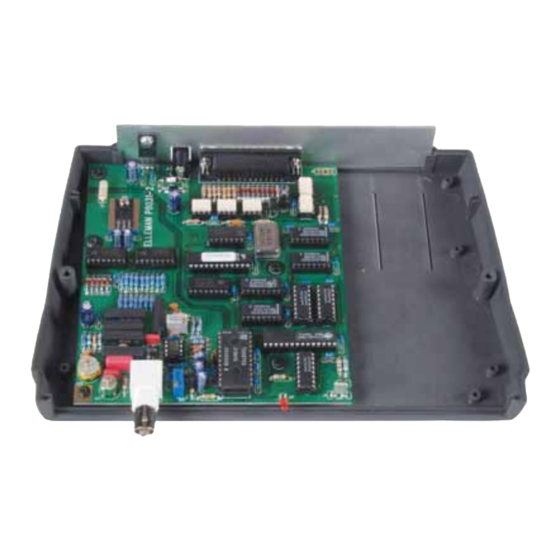
- Page 5 Construction The unit consists out of one main PCB with all the components Tip: The pictures on the packaging can be used as a guideline. However, due to possible changes it is not 100% reliable. Mount the components in the order described: : 91K (9-1-0-2) 1% 1.
- Page 6 Construction R44 : 2K2 (2-2-2) C47 : 100n (104, 0.1, u1) R45 : 820R (8-2-0-0) 1% C48 : 100n (104, 0.1, u1) R46 : 1K8 (1-8-2) R47 : 100R (1-0-1) 4. Capacitors R48 : 100R (1-0-1) R49 : 100R (1-0-1) R50 : 470R (4-7-1) C...
- Page 7 Construction 6. Electrolytic capacitors. Check 9. Trimmer capacitors the polarity ! C2 : 4µ7 C7 : 4µ7 C11 : 4µ7 C... C35 : 4µ7 C37 : 4µ7 CV... C44 : 4µ7 C23 : 100µF C43 : 100µF C46 : 100µF CV1 : 22p (small type) CV2 : 50p 7.
- Page 8 Construction 12. Reed relays (check the posi- 15. DC jack tion of the notch) RY... SK... + RY1 : VR05R051AS RY2 : VR05R051AS RY3 : VR05R051AS RY4 : VR05R051AS RY5 : VR05R051AS J2 : DJ-005 13. PCB tab 16. Power indication LED, comes later through the front panel LD : 3mm LED SK...
- Page 9 Construction 18. 25P sub D connector J6 : 25P sub D male 19. IC’s check the position ! : 74F161 : OPA2350PA : TDA8703 : 6264 ; CY7C199..EQ : 74HC153 : 74F161 : 74F161 : 74HC595 IC10 : 74HC85 IC11 : 74HC595 IC12 : 74HC595 R...
- Page 10 Construction 20. Screen foil preparation Cut the screening foil like in the drawing. Make sure the conductive side is faced downwards !! 20mm 80mm 10mm Fig. 1.0 Position the screen foil into the bottom enclosure. Use some adhesive tape to fix the screen foil Fig.
- Page 11 Construction 21. Voltage regulator and PCB assembly IC23: 7805 (UA7805P) - This regulator must be isolated plastic type ! Mount the voltage regulator on the rear panel and fasten it with the supplied M3 bolt, washer and nut as shown on the drawing. Make sure to remove the pro- tective foil from the front and rear panel! M3 BOLT Fig.
- Page 12 Construction 22. PCB and screen foil fixation Make sure the conductive side is faced downwards ! Tape* Fig. 1 Fix the screen foil using a washer and screw. (Push the screw through the foil) The conductive side must make contact with the PCB surface. * Please note that you should tape both front and back of the three visible edges in order to avoid all contact between the screening foil and the components.
- Page 13 • Connect a 9V/500mA power supply to the unit. (check the polarity). The LED on the front panel should lid. • Start the PC-Lab2000 software and select K8031 hardware and the appropri- ate port. • Short circuit the input using an appropriate probe or connection.
- Page 14 24. PCB...
- Page 15 Schematic diagram 25. Digital selection...
- Page 16 Opto coupler selection 26. Opto Coupler selection © Velleman Kit Values are for reference only...
- Page 17 Input selection 27. Input selection © Velleman Kit Values are for reference only...
- Page 18 Note :...
- Page 19 Note :...
- Page 20 VELLEMAN KIT NV Legen Heirweg 33 9890 Gavere Belgium Europe Info ?: http://www.velleman.be Questions ?: support@velleman.be Modifications and typographical errors reserved © Velleman Kit nv H8031IP - 2003 - ED1 5 4 1 0 3 2 9 2 9 1 0 4 4...
Need help?
Do you have a question about the K8031 and is the answer not in the manual?
Questions and answers