Table of Contents
Advertisement
Quick Links
LinkIt 7687 HDK V30 User's Guide
Version:
Release date:
© 2015 - 2016 MediaTek Inc.
This document contains information that is proprietary to MediaTek Inc. ("MediaTek") and/or its licensor(s). MediaTek cannot grant you
permission for any material that is owned by third parties. You may only use or reproduce this document if you have agreed to and been
bound by the applicable license agreement with MediaTek ("License Agreement") and been granted explicit permission within the License
Agreement ("Permitted User"). If you are not a Permitted User, please cease any access or use of this document immediately. Any
unauthorized use, reproduction or disclosure of this document in whole or in part is strictly prohibited. THIS DOCUMENT IS PROVIDED ON AN
"AS-IS" BASIS ONLY. MEDIATEK EXPRESSLY DISCLAIMS ANY AND ALL WARRANTIES OF ANY KIND AND SHALL IN NO EVENT BE LIABLE FOR ANY
CLAIMS RELATING TO OR ARISING OUT OF THIS DOCUMENT OR ANY USE OR INABILITY TO USE THEREOF. Specifications contained herein are
subject to change without notice.
1.3
30 June 2016
Advertisement
Table of Contents

Related Manuals for Mediatek Labs LinkIt 7687 HDK V30

Summary of Contents for Mediatek Labs LinkIt 7687 HDK V30
- Page 1 LinkIt 7687 HDK V30 User's Guide Version: Release date: 30 June 2016 © 2015 - 2016 MediaTek Inc. This document contains information that is proprietary to MediaTek Inc. (“MediaTek”) and/or its licensor(s). MediaTek cannot grant you permission for any material that is owned by third parties. You may only use or reproduce this document if you have agreed to and been bound by the applicable license agreement with MediaTek (“License Agreement”) and been granted explicit permission within the License...
- Page 2 LinkIt 7687 HDK V30 User's Guide Document Revision History Revision Date Description 31 March 2016 Initial version. 2 May 2016 Added power domain information. Refine the output binary file name. 17 May 2016 Added CMSIS-DAP firmware update procedure. 30 June 2016 Refine the Get started section and pull-up resister.
-
Page 3: Table Of Contents
LinkIt 7687 HDK V30 User's Guide Table of contents Introduction ............................4 Get started with the HDK ........................5 2.1. Configuring the LinkIt 7687 HDK ......................5 2.2. Installing the LinkIt 7687 HDK drivers on Microsoft Windows ............6 2.3. - Page 4 LinkIt 7687 HDK V30 User's Guide Lists of tables and figures Table 1. Jumper settings for system power input through USB connection ............10 Table 2. System power input from AA or AAA battery jumpers ................11 Table 3. GPIO pins to activate the LEDS ........................ 12 Table 4.
-
Page 5: Introduction
LinkIt 7687 HDK V30 User's Guide Introduction MediaTek LinkIt™ for real-time operating system (RTOS) is a low-cost and easy to use Internet of Things (IoT) development platform to design, prototype, evaluate and implement IoT projects. The platform supports LinkIt™ 76x7 hardware development kit (HDK) by SAC. This user manual provides required knowledge on features of the HDK, including the pins, communication interfaces, core microcontroller unit (MCU) description, the networking capabilities and how to use them through the host driver. -
Page 6: Get Started With The Hdk
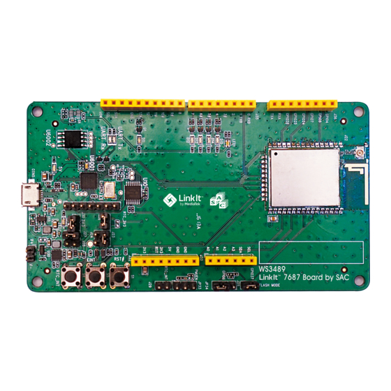
LinkIt 7687 HDK V30 User's Guide Get started with the HDK Before commencing the application development, you need to configure the development platform. 2.1. Configuring the LinkIt 7687 HDK LinkIt 7687 HDK includes a main board and a MT7687F stamp module. The MT7687F stamp module is mounted on the main board. -
Page 7: Installing The Linkit 7687 Hdk Drivers On Microsoft Windows
LinkIt 7687 HDK V30 User's Guide 2) Flash mode - Recovery mode. 3) Support RTC interrupt. 4) Clock source - 32.768kHz source crystal clock for the RTC mode or external clock operating on 32.768 kHz. 5) XTAL - 40MHz. 6) RTC mode - supported. -
Page 8: Configuring The Hdk Flash Mode
LinkIt 7687 HDK V30 User's Guide Figure 2. COM port associated with the LinkIt 7687 HDK 2.3. Configuring the HDK flash mode The LinkIt 7687 HDK is embedded with 2MB flash memory. The boot options are either from the Flash memory or from the UART port. -
Page 9: Downloading The Image Using The Linkit 7687 Hdk As A Removable Storage
LinkIt 7687 HDK V30 User's Guide to the UART1 port of the chipset and the code is uploaded to the embedded flash memory through UART1. 2) Connect the board to the computer using a micro-USB cable. The development board should now be connected to the PC, as shown in Figure 1. -
Page 10: Hardware Features
LinkIt 7687 HDK V30 User's Guide Hardware Features This section provides the main supported features of the LinkIt 7687 HDK. The detailed description of the features is provided in the upcoming sections. • IEEE 802.11bgn Wireless Connectivity Single Chip with QFN68 package. -
Page 11: Hardware Feature Configuration
LinkIt 7687 HDK V30 User's Guide Hardware Feature Configuration 4.1. Microcontroller MT7687F features an ARM Cortex-M4 with floating point processor, which is the most energy efficient ARM processor available. MT7687F provides low power consumption embedded architecture and it’s optimized for various types of applications in home automation, smart grid, handheld devices, personal medical devices and industrial control that have lower data rates, and transmit or receive data on an infrequent basis. -
Page 12: Leds
LinkIt 7687 HDK V30 User's Guide Figure 4. Power up the HDK using an AA or AAA Battery (J21) Table 2. System power input from AA or AAA battery jumpers Jumper Usage Comments 3.3V power supply Use AA or AAA battery source supporting 3.3V power. -
Page 13: Buttons
LinkIt 7687 HDK V30 User's Guide D9 (UART Tx) D10 (UART Rx) Figure 5. On-board LEDs 5) D11, D12, D13, D14, and D15 are LEDs assigned for user interaction. All LEDs are high active (Figure 5). GPIO pins to activate the LEDs are shown in Table 3. -
Page 14: Extension Connectors
LinkIt 7687 HDK V30 User's Guide 2) RTC interrupt mode button (S4). When the system is in the RTC mode, push the button to wake up the system. 3) External interrupt button (S5). Users can configure GPIO0 as an external interrupt pin. Press the button to wake up the system from the sleep mode. - Page 15 LinkIt 7687 HDK V30 User's Guide PWM[1] Pulse-width-modulated output EINT[1] External interrupt UART1_RX_CM4 UART1 RX (Cortex-M4) GPIO2 SWD_CLK Cortex-M4 SWD debug port GPIO[2] General purpose input, output PWM[23] Pulse-width-modulated output WIC[0] External interrupt UART1_TX_CM4 UART1 TX (Cortex-M4) GPIO3 SWD_DIO Cortex-M4 SWD debug port...
- Page 16 LinkIt 7687 HDK V30 User's Guide FRAME_SYNC * 3DD synchronization WIC[1] External interrupt SPI_SCK_M_CM4 SPI master SCK GPIO26 SPI_CLK_EXT * External flash interface I2S_TX I2S master TX GPIO[26] General purpose input, output PWM[27] Pulse width modulation SWD_DIO Cortex-M4 SWD debug port...
- Page 17 LinkIt 7687 HDK V30 User's Guide WIC[4] External interrupt SWD_DIO Cortex-M4 SWD debug port GPIO33 IR_TX IrDA TX GPIO[33] General purpose input, output PWM[34] Pulse width modulation PULSE_CNT Pulse counter WIC[5] External interrupt SWD_CLK Cortex-M4 SWD debug port GPIO34 IR_RX...
- Page 18 LinkIt 7687 HDK V30 User's Guide ADC_IN0 Auxiliary ADC input PCM_SYNC PCM interface for Bluetooth GPIO58 GPIO[58] General purpose input, output PWM[37] Pulse-width-modulated output WIC[9] External interrupt ADC_IN1 Auxiliary ADC input PCM_OUT PCM interface for Bluetooth GPIO59 SWD_DIO Cortex-M4 debug port...
-
Page 19: Rtc
LinkIt 7687 HDK V30 User's Guide Figure 7. Locations of I2C pull-up resistors 4.6. The LinkIt 7687 HDK features an RTC module. The clock source operates at 32.768kHz crystal oscillator or an external clock source. The RTC has built-in accurate timer to wake up the system when the user defined timer expires. -
Page 20: Cmsis-Dap Firmware Update Procedure
LinkIt 7687 HDK V30 User's Guide Figure 8. Location of the components C93 and C94 4.8. CMSIS-DAP Firmware update procedure The latest firmware from OpenSDA platform can be downloaded from the mbed official website. To update the binary firmware of CMSIS-DAP, press and hold the S1, then plug-in the USB cable to CON5, release the button S1 once the mass storage is shown, and then drag and drop in the binary code. -
Page 21: Schematics (V30)
LinkIt 7687 HDK V30 User's Guide Schematics (V30) Main board schematic-1 IC Power Consumption Measurement 5V_TEST RTC_3V3 EXT_PMU_EN PMU_EN_RTC NI/R/0/Ohm/0603 LED Green PMU_EN_WF SY S_RST_N GPIO0 DC_DC_3V3 3V3_IN C149 C150 C/0.1/uF/0402 C/4.7/uF/0603 V_2AA_O_3V3 R/15K/Ohm/0402 C181 C/10/uF/0805 LED Green PMU_EN_WF_D R/4.7K/Ohm/0402... - Page 22 LinkIt 7687 HDK V30 User's Guide Main board schematic-2 USB2 USB1 3.3V_I 3.3V_I R/1K/Ohm/0402 GPIO37_H R/1K/Ohm/0402 GPIO6_H GPIO0 GPIO1 GPIO2 GPIO3 GPIO4 JP34 3.3V_I I2C0 SCL GPIO27 GPIO5 GPIO6 I2C0 SDA GPIO28 GPIO6 3.3V_I GPIO7 GPIO37 SY S_RST_N GPIO24 3.3V_I...
- Page 23 LinkIt 7687 HDK V30 User's Guide Main board schematic-3 DC_DC_3V3 U6601 SDA_JTAG_TCLK VDD1 JTAG_TCLK/SWD_CLK/EZP_CLK/TSI0_CH1/PTA0/UART0_CTS/UART0_COL/FTM0_CH5 SDA_JTAG_TDI JTAG_TDI/EZP_DI/TSI0_CH2/PTA1/UART0_RX/FTM0_CH6 SDA_JTAG_TDO JTAG_TDO/TRACE_SWO/EZP_DO/TSI0_CH3/PTA2/UART0_TX/FTM0_CH7 SDA_JTAG_TMS VDDA JTAG_TMS/SWD_DIO/TSI0_CH4/PTA3/UART0_RTS/FTM0_CH0 SDA_SWD_EN NMI/EZP_CS/TSI0_CH5/PTA4/FTM0_CH1 C184 C / 1 / uF / 0402 CON5 VSSA CON / 5 / 000010801-0000/MAINSUPER MICROUSB/5P/SMD/000010801-0000/MAINSUPER TP6604...
- Page 24 LinkIt 7687 HDK V30 User's Guide Main board schematic-4 USER LED 3.3V_I D11 LED Green R/510/Ohm/0402 GPIO31_D GPIO31_L 3.3V_I 2SK3019_ROHM D12 LED Red R/510/Ohm/0402 R/10K/Ohm/0402 GPIO35_D GPIO35_L LED1 GPIO31 GPIO31_G SMLP36RGB1W 2SK3019_ROHM D13 LED Red R/510/Ohm/0402 GPIO34_D GPIO34_L R/10K/Ohm/0402 GPIO35...
Need help?
Do you have a question about the LinkIt 7687 HDK V30 and is the answer not in the manual?
Questions and answers