Table of Contents
Advertisement
Quick Links
Advertisement
Table of Contents

Related Manuals for Mesa 7I90HD


Summary of Contents for Mesa 7I90HD
- Page 1 7I90HD EPP/SPI/SERIAL ANYTHING I/O MANUAL Version 1.7...
- Page 2 This page intentionally not blank...
-
Page 3: Table Of Contents
CONNECTOR LOCATIONS AND DEFAULT JUMPER POSITIONS ..4 7I90HD I/O CONNECTOR PIN-OUT ....... . 5 POWER CONNECTOR PIN-OUT . - Page 4 INFO AREA ACCESS ........28 7I90HD SUPPORTED MEMORY SPACES ..... 29 SPACE0: HOSTMOT2 REGISTERS .
-
Page 5: General
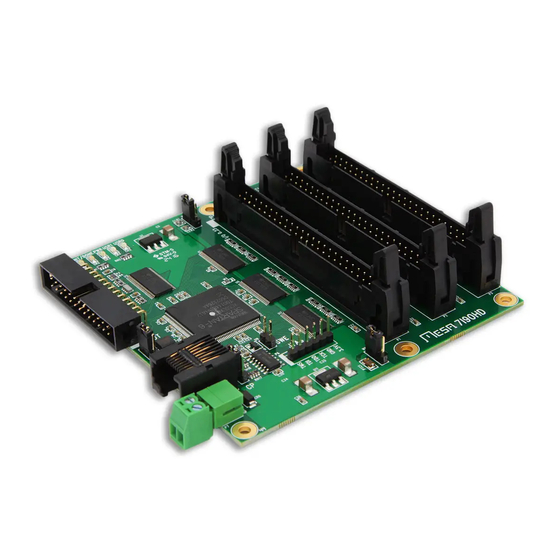
Socketed pullup resistors are provided for all pins so that they may be connected directly to opto-isolators, contacts etc. The 7I90HD has 72 I/O bits available on three 50 pin connectors, all connectors use I/O module rack compatible pinouts and are compatible with all Mesa 50 pin FPGA daughtercards. -
Page 6: Hardware Configuration
The FPGA used on the 7I90HD has a 4V absolute maximum input voltage specification. To allow interfacing with 5V inputs, the 7I90HD has bus switches on all I/O pins. The bus switches work by turning off when the input voltage exceeds a preset threshold. -
Page 7: Fpga Flash Select
That is, if one flash memory is inadvertently corrupted, the other one can be used to boot the 7I90HD, allowing the corrupted flash memory to be re-written. It is suggested that W3 be left in the UP position (primary flash memory) for normal operation, and only changed to the DOWN position (secondary flash memory) if configuration fails. -
Page 8: Connectors
CONNECTORS CONNECTOR LOCATIONS AND DEFAULT JUMPER POSITIONS 7I90HD... -
Page 9: 7I90Hd I/O Connector Pin-Out
CONNECTORS I/O CONNECTORS The 7I90HD has 3 I/O connectors, P1 through P3. 7I90HD IO connector pinouts are as follows: P1 CONNECTOR PINOUT FUNC FUNC FUNC FUNC IO10 IO11 IO12 IO13 IO14 IO15 IO16 IO17 IO18 IO19 IO20 IO21 IO22 IO23... - Page 10 CONNECTORS I/O CONNECTORS P2 CONNECTOR PINOUT FUNC FUNC FUNC FUNC IO24 IO25 IO26 IO27 IO28 IO29 IO30 IO31 IO32 IO33 IO34 IO35 IO36 IO37 IO38 IO39 IO40 IO41 IO42 IO43 IO44 IO45 IO46 IO47 POWER 7I90HD...
- Page 11 CONNECTORS I/O CONNECTORS P3 CONNECTOR PINOUT FUNC FUNC FUNC FUNC IO48 IO49 IO50 IO51 IO52 IO53 IO54 IO55 IO56 IO57 IO58 IO59 IO60 IO61 IO62 IO63 IO64 IO65 IO66 IO67 IO68 IO69 IO70 IO71 POWER 7I90HD...
-
Page 12: Power Connector Pinout
P6 is a JTAG programming connector. This is normally used only for debugging or if both EEPROM configurations have been corrupted. In case of corrupted EEPROM contents the EEPROM can be re-programmed using Xilinx’s Impact tool. P6 JTAG CONNECTOR PINOUT FUNCTION +3.3V 7I90HD... -
Page 13: Epp/Spi Connector Pin-Out
DB25 printer port pin-out, allowing a simple flat cable with a DB25M IDC connector on one end and a 26 pin female header on the other end to interface the hosts printer port to the 7I90HD. P4 PIN... -
Page 14: Rs-422 Connector Pin-Out
J1s pinout is designed to match breakout cards like the 7I44 and 7I74. A standard CAT5 or CAT5E cable can be used to connect the 7I90HD to a 7I44/7I74. CAT5E cable is suggested if the serial cable is used for powering the 7I90HD, as the larger wire size result in lower voltage drop. -
Page 15: Operation
SOCs. LBP is a simple binary serial master slave protocol. The LBP implementation in the 7I90HD allows the 7I90HD to be use as a simple 72 I/O Smart Serial slave for remote TTL level interfacing. -
Page 16: Epp Host Interface
OPERATION EPP HOST INTERFACE The EPP host interface option allows the 7I90HD to connect to EPP compatible parallel port on PCs for a medium speed real time interface. The interface from host EPP printer port to the FPGA uses 12 FPGA pins. These consist of an eight bit bidirectional data bus (D0..D7), and four handshake lines. -
Page 17: Spi Host Interface
The host interface uses the convention that the clock idles low, host data is shifted into the 7I90HD on the SPI clock rising edge, and data is shifted out of the 7I90HD on the clock falling edge. This matches SPI master setup with CPOL=0 and CPHA=0. The CS pin is active low. - Page 18 BURST TIMEOUT Because the 7I90HD’s SPI interface supports burst transfers of programmable length, its possible that an aborted or incorrect command could leave the 7I90HD in an unknown state. To recover from this condition, the 7I90HDs SPI interface has a timeout on bursts.
-
Page 19: Lbp16 Host Interface
Note that setting the low baud rate option sets the packet framing timeout to 25 character times instead of the normal 2 character times. This is to make access easier with standard serial ports and USB/serial adapters. PROTOCOL For detailed information on the LBP16 serial protocol, see the reference section of this manual 7I90HD... -
Page 20: Pc Serial Host Adapter
In order to run any of the serial command line utilities a RS-422 adapter is needed. Mesa can provide a suitable adapter. Two such adapters are 3I21 or 3I22. These adapters connects the RJ-45 RS-422 interface on the 7I90HD to a DB9 serial port (3I21) or USB port (3I22) and provide 5V link power. -
Page 21: Configuration
The second backup method relies on the fact that there are two flash memories on the 7I90HD card, selectable via jumper W3. If a configuration fails in such a way that it loads correctly (has a valid CRC) but does not work, the fallback configuration will not be invoked. -
Page 22: Eeprom Layout
OPERATION EEPROM LAYOUT The EEPROMs used on the 7I90HD for configuration storage are Micron M25P80's. The M25P80 is a 8 M bit (1 M byte) EEPROM with sixteen 64K byte sectors. Configuration files are stored on sector boundaries to allow individual configuration file erasing and updating. -
Page 23: Bitfile Format
Linux and Windows utility programs mesaflash and mesaflash.exe are provided to write configuration files to the 7I90HD EEPROM via the RS-422 interface and LBP16. The linux utility can also write configuration files via the EPP interface. These files depend on a simple SPI interface built into both the standard user FPGA bitfiles and the fallback bitfile. -
Page 24: Free Eeprom Space
JTAG connector or (faster) JTAG FPGA load followed by EPP or LBP16 EEPROM update. CLOCK SIGNALS The 7I90HD has a single 50 MHz clock signal from an on card crystal oscillator. The clock a can be multiplied and divided by the FPGAs clock generator block to generate a wide range of internal clock signals. -
Page 25: Leds
OPERATION LEDS The 7I90HD has two FPGA driven user LEDs (User 0 and User 1 = Green), and three status LEDs (two red and one yellow). The user LEDs can be used for any purpose, and can be helpful as a simple debugging feature. A low output signal from the FPGA lights the LED. -
Page 26: Supplied Configurations
12 PWM outputs, a watchdog timer and GPIO. SV6_7I49 SV6_7I49 is a six axis servo configuration for use with the 7I49 resolver input daughter card. Its has a 6 channel resolver interface, 6 pwm channels, a watchdog timer and GPIO. 7I90HD... -
Page 27: Pin Files
Each of the configurations has an associated file with file name extension .pin that describes the FPGA functions included in the configuration and the I/O pinout. These are plain text files that can be printed or viewed with any text editor. 7I90HD... -
Page 28: Reference Information
LBP16 read commands are followed by the 16 bit address (if the A bit is set). LBP16 Write commands are followed by the address (if bit A is set) and the data to be written. LBP16 Addresses are always byte addresses. LBP data and addresses are little endian so must be sent LSB first. 7I90HD... -
Page 29: Lbp16 Crc
The CRC polynomial is X^16 +X^12 +X^5 +1 (CRC-CCITT) The varient used is CRC-CCITT-KERMIT. FRAMING Packet framing in accomplished with timed gaps in transmitted data. Default packet frame timeout is 2 character times at high baud rates and 25 character times at 115200 baud. 7I90HD... -
Page 30: Info Area
Is type: 01 = Register, 02 = Memory, 0E = EEPROM, 0F = Flash Is access types (bit 0 = 8 bit, bit 1 = 16 bit etc)so for example 0x06 means 16 bit and 32 bit operations allowed 7I90HD... -
Page 31: Info Area Memranges Format
REFERENCE INFORMATION LBP16 INFO AREA MEMRANGES FORMAT Is erase block size Is Page size Ps address range Ranges are 2^E, 2^P, 2^S. E and P are 0 for non-flash memory 7I90HD... -
Page 32: Info Area Access
Ispace 4 read NN21 Ispace 5 read with address NN75LLHH Unused Ispace 5 read NN75 Ispace 6 read with address NN79LLHH LBP16 R/W space Ispace 6 read NN39 Ispace 7 read with address NN7DLLHH LBP16 R/O space Ispace 7 read NN3D 7I90HD... -
Page 33: 7I90Hd Supported Memory Spaces
LBP16 7I90HD SUPPORTED MEMORY SPACES The 7I90HD firmware supports 7 address spaces. These will be described individually with example hexadecimal commands. The hex command examples below are written in LSB first order for convenienc5901e. In the hex command examples, the NN is the count/increment field of the LBP16 command and the LLHH is the low and high bytes of the address. - Page 34 ; 32 bit data for GPIO port 0 at 0x1000 BBBBBBBB ; 32 bit data for GPIO port 0 at 0x1004 CCCCCCCC ; 32 bit data for GPIO port 0 at 0x1008 Note: like all LBP16 data, write data is LS byte first. 7I90HD...
-
Page 35: Space3: Fpga Flash Eeprom Chip Access
The page write is started by writing the flash address, reading the flash address, reading flash data, reading flash ID or issuing a erase sector command. For host synchronization, a read operation should follow every sector erase or page write. 7I90HD... - Page 36 Issue write flash data command with count 12345678 Doubleword 0 ABCD8888 Doubleword 1 FFFFFFFF Doubleword 63 (= 256 bytes) 014E0000 Read new address to commit write and so some data is returned for host synchronization (so host waits for write to complete) 7I90HD...
- Page 37 Write EEPROMWEna with 0x5A03 01CE000000000100 Write flash address with 0x 00010000 01CE0C0000000000 Write sector erase command (with dummy 32 bit data = 0) 014E0000 Read flash address for host synchronization (this will echo the address _after_ the sector is erased) 7I90HD...
-
Page 38: Space4: Lbp Timer/Util Registers
The HM2TimeOut register places an upper bound on how long the WaitForHM2 operations will wait. HM2Timeouts set the HM2TImeout error bit in the error register. 7I90HD... -
Page 39: Space6: Lbp Status/Control Registers
Space 6 write with address NND9LLHHDDDD Space 6 read NN19 Space 6 write NN99DDDD MEMORY SPACE 6 LAYOUT: ADDRESS DATA 0000 ErrorReg 0002 LBPParseErrors 0004 LBPMemErrors 0006 LBPWriteErrors 0008 RXPktCount 000A RXGoodCount 000C RXBadCount 000E TXPktCount 0010 TXGoodCount 0012 TXBadCount 7I90HD... -
Page 40: Error Register Format
Note that this is cleared at the end of every packet. 001C LBPReset Setting this to a non-zero value with do a full reset of the LBP16 firmware. The 7I90HD will be unresponsive for as much as ½ a second after this command. ERROR REGISTER FORMAT ERROR... -
Page 41: Space7: Lbp Read Only Information
0006 CardNameChar-6,7 0008 CardNameChar-8,9 000A CardNameChar-10,11 000C CardNameChar-12.13 000E CardNameChar-14,15 0010 LBPVersion 0012 FirmwareVersion 0014 Option Jumpers 0016 Reserved 0018 RecvStartTS 1 uSec timestamps 001A RecvDoneTS For performance monitoring 001C SendStartTS Send timestamps are 001E SendDoneTS from previous packet 7I90HD... -
Page 42: Specifications
INPUT VOLTAGE (5V mode) -0.6V ---- 0.5V 20 mA sink ---- 2.8V 20 mA source (3.3V mode) RS-422 DATA RATE ---- 10 MBaud MAX 5V CURRENT TO I/O CONNS 400 mA Each (PTC Limit) TEMPERATURE RANGE -C version TEMPERATURE RANGE -I version 7I90HD... -
Page 43: Card Drawing
REFERENCE INFORMATION CARD DRAWING 7I90HD...
Need help?
Do you have a question about the 7I90HD and is the answer not in the manual?
Questions and answers