Table of Contents
Advertisement
Advertisement
Table of Contents

Related Manuals for Mesa 7I76


Summary of Contents for Mesa 7I76
- Page 1 7I76 STEP/DIR PLUS I/O DAUGHTERCARD V1.22...
-
Page 3: Table Of Contents
CONNECTORS ............3 7I76 CONNECTOR LOCATIONS AND DEFAULT JUMPER POSITIONS ..3 HOST INTERFACE CONNECTOR . - Page 4 Table of Contents OPERATION FIELD I/O ........... . 13 FIELD AND VIN POWER SUPPLY .
- Page 5 PROCESS ELEMENT PACKING AND UNPACKING ... . . 32 7I76 SPECIFIC PROCESS DATA EXAMPLE ....33 NORMAL MODE OPERATION .
- Page 6 Table of Contents REFERENCE INFORMATION ........41 LBP .
-
Page 7: General
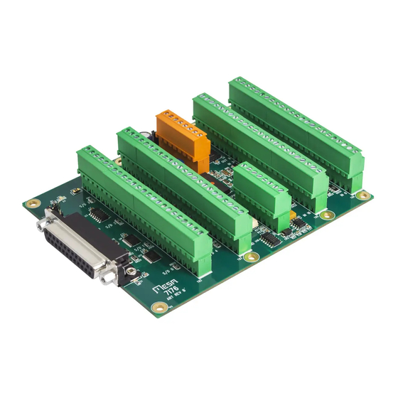
The 7I76 is daughtercard/breakout board for use with MESA's 25 pin I/O FPGA cards like the 5I25. The 7I76 is designed for interfacing up to 5 Axis of step &dir step motor or servo motor drives and also provides a spindle encoder interface, isolated analog spindle speed control and 48 isolated I/O points for general purpose field I/O use. -
Page 8: Hardware Configuration
If W2 is in the left hand position, host cable power is used. If W2 is in the right hand position, 5V power must be supplied to the 7I76 via TB3. This option must be set to match the cable power option of the host FPGA card. If the FPGA card supplies 5V, W2 must be in the left hand position. -
Page 9: Connectors
CONNECTORS 7I76 CONNECTOR LOCATIONS AND DEFAULT JUMPER POSITIONS 7I76 3... -
Page 10: Host Interface Connector
2. GPIO pins are for first FPGA connector, next connector series begins at GPIO17 3. Signal directions are relative to FPGA card, that is, an ‘OUT’ signal is an output from the FPGA card that drives the 7I76. Conversely an ‘IN’ signal is a FPGA input that is driven by the 7I76. -
Page 11: Tb2 Step And Dir Connector
SIGNAL TB2 PIN SIGNAL STEP0- STEP2- STEP0+ STEP2+ DIR0- DIR2- DIR0+ DIR2+ +5VP +5VP STEP1- STEP3- STEP1+ STEP3+ DIR1- DIR3- DIR1+ DIR3+ +5VP +5VP Note: 5VP pins are PTC short circuit protected 5V output pins for field wiring. 7I76 5... -
Page 12: Tb3 Step/Dir, Encoder And Rs-422 Connector
STEP4+ DIR4- RS-422 RX+ DIR4+ RS-422 RX- +5VP RS-422 TX+ ENCA+ RS-422 TX- ENCA- +5VP 5V supply power ENCB+ 5V supply power ENCB- +5VP Note: 5VP pins are PTC short circuit protected 5V output pins for field wiring. 7I76 6... -
Page 13: Tb4 Spindle Connector
TB4 is the spindle drive interface with isolated analog output and control signals for a spindle interface.TB4 is a 8 terminal 3.5 MM pluggable terminal block with supplied removable screw terminal plugs. TB4 PINOUT TB4 PIN SIGNAL SPINDLE- SPINDLE OUT SPINDLE+ SPINDLE ENA- SPINDLE ENA+ SPINDLE DIR- SPINDLE DIR+ 7I76 7... -
Page 14: Field Input/Output Connectors
0 through 15 and outputs 0 through 7 are terminated at TB6. Inputs 16 through 31 and outputs 8 through 15 are terminated at TB5. TB6 and TB5 are 3.5 MM pluggable terminal block with supplied removable screw terminal plugs. Pin one is at the bottom edge of the 7I76 card. TB6 CONNECTOR PINOUT TB6 PIN... -
Page 15: Tb5 Pinout
CONNECTORS FIELD INPUT/OUTPUT CONNECTORS TB5 CONNECTOR PINOUT TB5 PIN OUTPUT TB5 PIN OUTPUT INPUT16 INPUT28 INPUT17 INPUT29 INPUT18 INPUT30 INPUT19 INPUT31 INPUT20 OUTPUT8 INPUT21 OUTPUT9 INPUT22 OUTPUT10 INPUT23 OUTPUT11 INPUT24 OUTPUT12 INPUT25 OUTPUT13 INPUT26 OUTPUT14 INPUT27 OUTPUT15 7I76 9... -
Page 16: Field Power Connector
LOGIC POWER 8-32V GROUND VIN, VFIELD, COMMON (Top pin) Note: When W1 is in the default left hand position, VIN is connected to VFIELD, so only VFIELD need be supplied to the 7I76 to power its field IO. 7I76 10... -
Page 17: Operation
I/O expansion with Mesa SSERIAL devices. The easiest way to make a cable for interfacing the 7I76 to these devices is to take a standard CAT5 or CAT6 cable, cut it in half, and wire the individual wires to the 7I76 screw terminals. The following chart gives the... -
Page 18: Encoder Interface
The 7I76 has two yellow status LEDs for power monitoring, CR1 and CR2. CR1 on the top left side of the 7I76 monitors 5V power. CR2 on the top right side of the 7I76 monitors field power. Both LEDs must be illuminated for normal operation. -
Page 19: Field I/O
5V field voltage is used. Power consumption is approximately 600 mW or 25 mA at 24V. VIN power must be present for the 7I76 field I/O to be detected and operate. Field voltages that are too high or too low will cause faults. -
Page 20: Maximum Per Chip Current
It is suggested that inputs like limit switches use normally closed switches with one switch leg connected to field power and the other to the 7I76 input pin, so the normal machine state (not at limits) is to have the inputs activated. This way, a open switch wire or wire shorted to ground will cause a detectable machine fault. -
Page 21: Watchdog And Faults
OPERATION FIELD I/O WATCHDOG AND FAULTS The 7I76 has a watchdog timer that will set all set a fault flag if host communication does not occur at a minimum rate. Default watchdog time is 50 mS which means if not accessed at a greater than 20 Hz rate, the watchdog will bite and disable the outputs. -
Page 22: Non-Volatile Field I/O Parameters
EEPROM and are copied to the volatile working parameters at power-up. Because of this, non-volatile parameters only take affect after a 7I76 power cycle. OPERATE MODE BAUD RATE The operate mode baud rate default is 2.5 MBaud. This should not be changed unless needed for non-standard applications. -
Page 23: Rpd, Wpd, And Uflbp
7I76 parameters, and updating the firmware on the 7I76 To use these utilities on most operating systems, the 7I76 must be in the setup mode or the operate mode baud rate must be 115200 KBaud or less RPD, WPD, and UFLBP need environment variables preset before they will work. -
Page 24: Software Process Data Modes
The 7I76 has three software selectable process data modes. These different modes select different sets of 7I76 data to be transferred between the host and the 7I76 during real time process data exchanges. For high speed applications, choosing the correct mode can reduce the data transfer sizes, resulting in higher maximum update rates. -
Page 25: Reference Information
SSLBP GENERAL SSLBP is a firmware option to HostMot2s SSERIAL serial interface that allows simple communication to LBP based peripherals like the 7I76. SSERIAL is a part of the HostMot2 motion interface firmware for MESA’s Anything-I/O FPGA cards. REGISTER MAP SSLBP has two global processor interface registers and four per channel remote device interface registers. -
Page 26: Command Register
The command register has a feature that any command written with the MSB (bit 31) set will be ignored. This is for compatibility with DMA driven interfaces or any interfaces that use a fixed address list for low level hardware access so cannot skip writes. 7I76 20... -
Page 27: Data Register
1. The host polls the command register until it reads as zero. 2. The host writes the data byte to the data register 3. The host writes the command register with the the parameter address Ored with both the Request bit (bit 13) and the Write bit (bit 15) 7I76 21... -
Page 28: Local Parameters
0x0003 Minor SSLBP firmware revision GP_INPUTS 0x0004 Number of GP input bits (0 for SSLBP) GP_OUTPUTS 0x0005 Number of GP output bits (0 for SSLBP) PROCESSOR_TYPE 0x0006 0xD8 for Dumb8 CHANNELS 0x0007 1 to 8 depending on configuration 7I76 22... -
Page 29: Normal Start
50 mS watchdog timeout period). If this is not done, the remote device’s watchdog will bite, disabling its outputs and setting the fault flag. This will require a channel stop followed by a channel start to resume normal operations. 7I76 23... -
Page 30: Stop All
The data register contents returned after a DOIT command can be used to minimize host access cycles by avoiding the need to read the per channel status registers. If detailed fault information is desired, the CS register can be read on any channel that shows a failed transfer. 7I76 24... -
Page 31: Per Channel Interface Data Registers
UNIT# BYTE 3 UNIT# BYTE 2 UNIT# BYTE 1 UNIT# BYTE 0 INTERFACE 1 NAME BYTE 3 NAME BYTE 2 NAME BYTE 1 NAME BYTE 0 GTOCP BYTE1 GTOCP BYTE 0 PTOCP BYTE1 PTOCP BYTE 0 INTERFACE 2 7I76 25... - Page 32 Byte0 = Local Communication faults (sticky, cleared only by STOP) Bit 7 = TooManyerrors Bit 6 = RemoteFault Bit 5 = SerialBreakError Bit 4 = ExtraCharacterError Bit 3 = TimeoutError Bit 2 = OverrunError Bit 1 = InvalidCookieError Bit 0 = CRCError 7I76 26...
-
Page 33: Cs Register After Start
3 of the CS register contains remote fault information: Byte3 = REMOTE_FAULTS Bit 7 = LBPCOMFault Bit 6 = IllegalMode Fault Bit 5 = LowVoltageFault Bit 4 = HighVoltageFault Bit 3 = OverCurrentFault Bit 2 = OverTempFault Bit 1 = NoEnableFault Bit 0 = WatchdogFault 7I76 27... -
Page 34: Process Data Discovery
Note to the bewildered: process data discovery and its complications are not needed to access the 7I76 via SSLBP. In fact the 7I76's data can be accessed via SSLBP with no more than a few register reads and writes The sole purpose of process data discovery is to allow the driver to present nicely named and formatted data to the host without the driver having any built in knowledge of the remote device. -
Page 35: Process Data Descriptor
The DATA_LENGTH field is a single byte field that specifies the length of the process data element in bits. Minimum is 1 bit, maximum is 255 bits, however current SSLBP implementations are limited by the number of interface registers to a maximum of 96 bits. 7I76 29... -
Page 36: Data_Type
The PARAMETER_MAX field is a 32 bit IEEE-754 floating point number that specifies the maximum value of the process data element. This is to allow the driver to present data in engineering units. Not valid for non-numeric data types. 7I76 30... -
Page 37: Unit_String
8 BITS UNUSED MODE_NAME_STRING VARIABLE NULL TERM. STRING MODE TYPES Currently there are only two mode types, HWMODE = 0x00 and SWMODE = 0x01 these correspond to hardware (EEPROM or Jumper setting )and software (dynamically changeable operational modes) 7I76 31... -
Page 38: Process Element Packing And Unpacking
OPD BYTE 2 OPD BYTE 1 OPD BYTE 0 INTERFACE 0 INTERFACE 1 OPD BYTE 7 OPD BYTE 6 OPD BYTE 5 OPD BYTE 4 INTERFACE 2 OPD BYTE 11 OPD BYTE 10 OPD BYTE 9 OPD BYTE 8 7I76 32... -
Page 39: 7I76 Specific Process Data Example
INTERFACE 2 IPD BYTE 11 IPD BYTE 10 IPD BYTE 9 IPD BYTE 8 7I76 SPECIFIC PROCESS DATA EXAMPLE Process data is remote device dependent and also dependent on remote device mode. The 7I76 supports 3 software modes. 7I76 33... - Page 40 REFERENCE INFORMATION SSLBP 7I76 SPECIFIC PROCESS DATA EXAMPLE In the default input/output mode the process data appears in the interface registers in the order shown: 7I76 OUTGOING PROCESS DATA FOR MODE (1) CS REG SPINOUT 15..8 SPINOUT 7..0 TB5 OUTS 15..8 TB6 OUTS 7..0...
-
Page 41: Normal Mode Operation
8. Read per channel Interface register 0 and interface register 1 for input process data 9. Write per channel output process data ( for 7I76) to interface 0 register and interface 1 register 10. Write DOIT command = 0x10NN where NN is the bit mask of channels to initiate transfers. -
Page 42: Setup Start
LBP device parameter. This allows simple utilities to setup 7I76 volatile and non-volatile parameters, and allows the host to do process data discovery to determine the input and output process data information from the remote device. -
Page 43: Remote Write Example
. Repeat from step 5 for any additional remote parameter writes Remote write byte, word, long and double are basically equivalent, the only difference being the LBP command (0x64,0x65,0x66,0x67 respectively) and the size of the data written to the interface register(s) 7I76 37... -
Page 44: Discovery Sequence
7. If word data is 0, PTOC collection is complete goto step 11 8. Save value in local PTOC table, and increment local PTOC table index 9. Increment PTOCP value by 2 (as it is a word pointer) 10. Repeat from step 6 7I76 38... - Page 45 (remote read byte at CharPointer, increment CharPointer, if byte is 0: done) 23 Read NAME_STRING starting at CharPointer repeat (remote read byte at CharPointer, increment CharPointer, if byte is 0: done) 24. Repeat with next PTOC = step 11 7I76 39...
- Page 46 27. Read MODE_NAME_STRING starting at PTOC+4 Initialize CharPointer to PTOC+4 repeat (remote read byte at CharPointer, increment CharPointer, if byte is 0: done) 28. Repeat with next PTOC = step 1 29. Select next channel # and repeat from step 5 7I76 40...
-
Page 47: Reference Information
Note that the low level serial interface details presented here are not normally needed for 7I76 card access, as all the low level details are handed by the SSLBP code in the SSerial interface built into the FPGA, but is presented here for completeness. -
Page 48: Example Commands
Write 2 more bytes (0xEE,0xFF) at 0x014 and 0x015: COMMAND BITS LBPWrite: 0 add 2 data Write data 0 Write data 1 Read 8 bytes at 0x010,0x011,0x012,0x013,0x014,0x015,0x016,0x017: COMMAND BITS LBPRead: 2 add 8 data Read Address LSB Read Address MSB 7I76 42... -
Page 49: Local Lbp Commands
BIT 3 Watchdog timeout error BIT 2 Reserved BIT 1 Reserved BIT 0 CRC error 0xC2 Get CRC enable status (note CRCs are always enabled on the 7I76) 0xC3 Get CRC error count 0xC4 .. 0xC9 Reserved 0xCA Get Enable_RPCMEM access flag 0xCB Get Command timeout (character times/10 for serial) 0xCC .. - Page 50 0xDA Get LBP version 0xDB Get LBP Unit ID (Serial only, not used with USB) 0xDC Get RPC Pitch 0xDD Get RPC SizeL (Low byte of RPCSize) 0xDE Get RPC SizeH (High byte of RPCSize) 0xDF Get LBP cookie (returns 0x5A) 7I76 44...
-
Page 51: Local Lbp Write Commands
0xF8 Set low address 0xF9 Set high address 0xFA Add byte to current address 0xFB .. 0xFC Reserved 0xFD Set unit ID (serial only) 0xFE Reset LBP processor if followed by 0x5A 0xFF Reset LBP parser (no data follows this command) 7I76 45... - Page 52 Bit 5..0 RPCNumber: Specifies RPC 0 through 63 In the 7I76 LBP implementation, RPCPitch is 0x8 bytes so each RPC command has native size of 0x08 bytes and start 0x8 byte boundaries in the RPC table area. RPCs can cross RPCPitch boundaries if larger than RPCPitch RPCs are needed. The stored RPC commands consist of LBP headers and addresses, and possibly data if the command header has the RID bit set.
-
Page 53: Example Rpc Command List
LBPRead: 2 add 2 data Read Address LSB Read Address MSB Terminator The data stream for this RPC would consist of these 3 bytes: COMMAND BITS RPC 5 Data 0 for Command 1 Data 1 for Command 1 7I76 47... -
Page 54: Special Rpcs
DiscoveryRPC. LBP on the 7I76 uses CRC checking of all commands and data to insure validity. The CRC used is a 8 bit CRC using the same polynomial as the Dallas/Maxim one wire devices (X^8+X^5++X^4+X^0). -
Page 55: Sserial Remote Rpcs
Discovery RPC indicates. As mentioned above, the first byte of data sent from the remote to the host is always remote fault information as listed in CS REGISTER AFTER DOIT section of the manual. The process data RPC is 0xBD hex. 7I76 49... -
Page 56: Specifications
Per output (INDUCTIVE LOADS WITH NO FLYBACK DIODE) PER DRIVER CHIP CURRENT ---- 1.4A Per chip HIGH SPEED ENCODER INPUT INPUT COMMON MODE RANGE Volts INPUT TTL MODE THRESHOLD Volts DIFFERENTIAL MODE IMPEDANCE Ohms COUNT RATE ---- 10 MHz 7I76 50... - Page 57 (SPINDLE+ B > SPINDLE-) SUPPLY CURRENT ---- ISOLATION VOLTAGE ---- Volts DC NON-LINEARITY ---- % at 5KHz DIR/ENA OUTPUT CURRENT ---- DIR/ENA OUTPUT VOLTAGE ---- Volts DC DIR/ENA ISOLATION VOLTAGE ---- Volts DC ENVIRONMENTAL TEMPERATURE -C VERSION TEMPERATURE -I VERSION 7I76 51...
-
Page 58: Drawings
DRAWINGS 7I76 52...
Need help?
Do you have a question about the 7I76 and is the answer not in the manual?
Questions and answers