Advertisement
Advertisement
Table of Contents

Related Manuals for Cobra 148GTL-DX


Summary of Contents for Cobra 148GTL-DX
- Page 1 Cobra Communications Product Group DYNASCAN CORPORATION 6460 W. Cortland Street Chicago, Illinois 60635...
- Page 2 о Cobra Communications Product Group DYNASCAN CORPORATION 6460 W. Cortland Street Chicago, Illinois 60635...
- Page 3 TABLE OF CONTENTS...
- Page 4 T H E C B S T O R Y HAVE A GOOD DAY TODAY A BETTER DAY TOMORROW!
- Page 5 Section I Introduction...
- Page 7 Section II Spécifications Transmit: Receiver:...
- Page 8 ßV ßV.
- Page 9 Section III Installation LOCATION MOUNTING THE CONNECTION...
- Page 10 IGNITION NOISE INTERFERENCE ANTENNA...
- Page 11 TUNING THE ANTENNA FOR OPTIMUM SWR A. Antennas with adjusîment screws (set screws). B. Antennas which must be eut to proper length. Be very careful not to eut too much at one time, as one it is eut, it сап по longer be lengthed.
- Page 12 BASE STATION OPERATION (Operating from 120V AC House Current) Extemal Speaker...
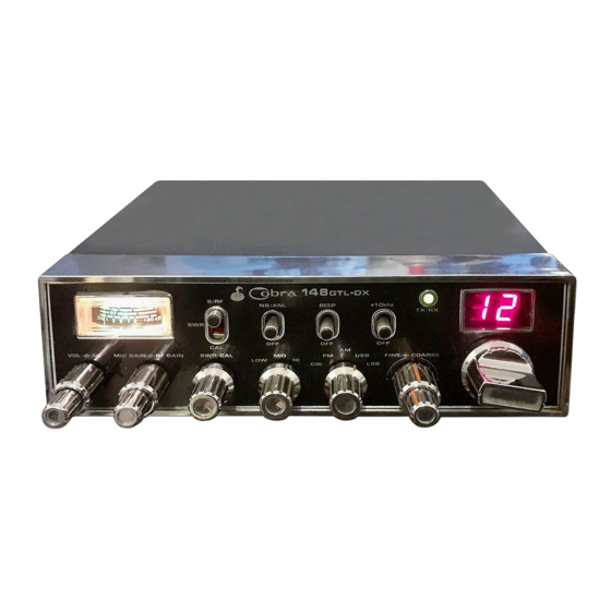
- Page 13 Section IV Operation CONTROLS AND INDICATORS A, CONTROL FUNCTIONS...
- Page 14 - ■...
- Page 15 В. INDICATOR FUNCTIONS OPERATING PROCEDURE TO RECEIVE...
- Page 16 OPERATING PROCEDURE TO TRANSMIT RECEIVING SSB SIGNALS half only...
- Page 18 OPERATING PROCEDURE TO CW(CARRIER WAVE) MODE I 1 i 2 i 1 : MARK SIGNAL ON NO SIGNAL ROGER ВЕЕР PRESS-TO-TALK OFF...
- Page 19 ALTERNATE MICROPHONES AND INSTALLATION...
- Page 20 Plug.
- Page 22 Section V Maintenance and Adjustment ----------------------------------- N0TE------------------------------------------...
- Page 23 Section VI Appendix 10 CODE Code Meaning Meaning Code Time is up for contact Receiving poorly 10-29 10-1 Receiving well 10-2 Does not conform to FCC Stop transmitting. 10-30 10-3 tules 10-4 OK, message received 10-32 I will give you a radio check Relay message 10-5 EMERGENCY TRAFFIC...
- Page 24 10 CODE (Continued) Code Meaning Code Meaning Proceed with transmission in 10-71 10-91 Talk doser to mikę sequence 10-93 Check my. frequency on this Negative contact 10-77 channel 10-94 Please give me a long count Reserve hotel ro om for Mission completed, all units 10-81 10-99...
- Page 25 HOW YOUR CB CAN SERVICE YOU...
- Page 26 U S E C H A N N E L 9 F O R EM E R G E N C Y M E SSA G E S O N L Y Permitted Example Message...
- Page 27 WARRANTY SERVICE INSTRUCTIONS Service Department - 2 6 -...
- Page 28 DYNASCAN will, without charge, repair or replace, at its option, defective radios or component parts upon delivery to an authorized COBRA service station or the factory service départaient, accompanied by proof of the date of purchase in the form of a sales receipt.
- Page 29 DYNASCAN CORPORATION P rin ted in T a iw a n...
- Page 30 SERVICE MANUAL 148 GTLDX (EARLY & LATE VERSIONS) COBRA COMMUNICATIONS PRODUCTION GROUP DYNASCAN CORPORATION 6460 W. CORTLAND ST. CHICAGO, ILLINOIS 60635...
-
Page 31: Table Of Contents
TABLE OF CONTENTS Early Version Page Description Block Diagram Schematic Diagram Wiring Diagram 8-13 Alignment Procedure 14-15 Parts Layout Top View 16-17 Copper Pattern Main PCB Bottcm View Added Parts Main PCB Bottcm View Copper Pattem SWR PCB CH SW PCB LED PCB Parts Layout Sub. - Page 32 со B L O C K D I A G R A M...
-
Page 33: Schematic Diagram
SCHEMATIC DIAGRAM... - Page 34 W IRING DIAGRAM P C - 8 8 I P C - 8 8 0 Y Y - 0 27 YEL 1 5 - 4 0 - 3 ____ •; • J 5 0 3 J 502 6 - 7...
-
Page 35: Alignment Procedure
C148GTL DX ALIGNMENT PROCEDURE ALIGNENT OF PLL AND CARRIER OSCILLATOR SECTION. 1. Test Equipment Required: Effectivity: S/N 03000001-4498 S/N 13000001-1504 a) Oscilloscope b) DC Voltmeter EARLY c) Frequency Counter VERSION 2. Alignment Procedure. ADJUSTMENT STEP PRESET ТО REMARKS LI 4 Connect Oscilloscope to TP4 (lead of R83). - Page 36 C148G7TL DX ALIGNMENT PROCEDURE STEP PRESET ТО ADJUSTMENT REMARKS Adjust for 16.0425MHz + or - 20Hz. Same as Step 8, : 40 Mode : USB Adjust for 16.0375MHz + or - 20Hz. Same as Step 9, : 40 Mode : LSB Adjust for 16.940MHz + or - 20Hz.
- Page 37 C148GLT DX A U G M E N T PROCEDURE A U G M E N T OF RECEIVER PORTION 1. Test Equipment Required a) SG, 27NHz Band. b) Osci lloscop>e. c) AF VTVM (Across 8oz. speaker). d) Deviation Meter. 2.
- Page 38 C148GTL DX ALIGNMENT PROCEDURE STEP PRESET ТО ADJUSTMENT REMARKS Same as Step 1 VRll Set the SG output level to lOOuV with No modulation. Then adjust VRl for S-9 read ing on radio's meter. Same as step 1 L9 and L10 Set the SG to lOuV with No-Modulation.
- Page 39 C148CTL DX ALIGNMENT PROCEDURE STEP PRESET ТО ADJUSTMENT REMARKS Restore PC-834. Turn the oore to the Same as Step 1, except: bottom. Mic Input: 30mV lKHz Same as Step 3 L64, L66, Adjust for maximum reading on RF VTVM and L67. (across 50ohm Dummy Load) .
- Page 40 C148GTL DX A L I G N E N T PROCEDURE ADJUSTMENT REMARKS STEP PRESET ТО Adjust for 4.5kHz déviation (FM Deviation Same as Step 1, except: Adj.). Mode : FM Band : Low 40 Mic Input: 30mV 1kHz Adjust 0.2V reading on AF VTVM when CW VR12 Same as Step 12 key is keyed.
- Page 41 P a r ts L a y o u t T o p V ie w 1 4 - 1 5...
-
Page 42: Parts Layout Top View
PARTS LAYOUT (Top View) - Page 43 ADDED PARTS - MAIN PCB (Bottom View) PC-879AB...
- Page 44 COPPER PATTERN SWR PCB CH SW PCB LED PCB...
-
Page 45: Parts Layout Sub. Assy Pcb's Top View
PARTS LAYOUT SUB. ASSY. PCB’s (Top View) P C — 8 8 0 AA CH SW P C B P C 9 5 8 А Д P C - 9 S $ A A SWR P C B... -
Page 46: Semi Conductor Pin Configuration
SEMI CONDUCTOR PIN CONFIGURATION TRANSISTOR BASE 1N60-AM В n o t e 1SS97 EMITTER CATHODE ANODE 1S2075K С: COLLECTOR MC-301 MARKING 1S2688EB MV-201 RD75EB2 2SC945A-Q 2SC1674L KB262 2SC1675L 2SC1730L 2SA733P CATHODE ANODE 1N4003 MARKING 2SC1312F 2SC2086D 2SB525C TLRG-101 MARKING SIDE iGREEN) 2SC1969B 2SC2166C... - Page 47 INTERNAL DIAGRAM - IC’s SCHEMATIC DIAGRAM CONNECTION INFORMATION Order Part No* LM 124D. LM 224D . LM 324D . LM 2902D , LM 224N. LM 324N . LM 2902N...
- Page 48 INTERNAL DIAGRAM - IC’s MB87I9...
- Page 49 INTERNAL DIAGRAM - IC’s го...
- Page 50 INTERNAL DIAGRAM - IC’s S 0 4 2 P...
- Page 51 VOLTAGE CHART îtode B a s e Collecter Einitter T R 5 R X C W U S B L S B N B /O N T X C W U S B IS B T R 6 R X C W U S B L S B N B /O N 7.6...
- Page 52 VOLTAGE CHART та ж...
- Page 53 VOLTAGE CHART та та та та от та та та та — от та та та та та та та та та та та та та ____ IV» С О...
- Page 54 VOLTAGE CHART г\э СО...
- Page 55 VOLTAGE CHART l.G~ _ f l _ Ш...
- Page 56 VOLTAGE CHART Mode 7.0 13.1 13.8 IC 5 7.0 13.1 13.8 7.0 13.1 13.8 7.0 13.1 13.8 7.0 13.1 13.8 6.9 13.0 13.7 10.9 13.4 10.9 13.4 11.4 13.7 11.4 13.7 -0.5 -0.5 IC 6 -0.5 -0.5 -0.5 -0.5 -0.5 -0.5 -0.5 -0.5...
-
Page 57: Block Diagram
TABLE OF CONTENTS Early Version Page Description Block Diagram Schematic Diagram Wiring Diagram Alignment Procedure Parts Layout Top View Copper Pattern Main PCB Bottcm View Added Parts Main PCB Bottcm View Copper Pattem SWR PCB CH SW PCB LED PCB Parts Layout Sub. - Page 58 B L O C K D I A G R A M...
- Page 59 SC H EM A TIC DIAGRAM P B - O I O...
- Page 60 W iRING DIAGRAM P C - 881 P C - 8 8 0 3 5 - 3 6...
- Page 61 C148GTL DX ALIGNIMENT PROCEDURE LATE VERSION Aiignment of PLL Portion. 1. Test Equipment Required a) Oscilloscope (0-5MHz). b) DC Voltmeter (10 Volts Max., 100k ohm/Volt). c) Frequency Counter. 2. Aiignment Procedure. STEP PRESET ТО ADJUSTMENT CONNECTIONS PROCEDURE RX. Mode. Connect Oscilloscope to Adjust for Max.
-
Page 62: Alignment Procedure
C148GTL DX ALIGNMENT PROCEDURE Alignment of Transmitter Section 1. Test Equipment Required a) VTVM (Fuli scalę; IV DC with RF Probe) b) RF Output Pcwer Meter. c) Spectrum Analyzer. d) Frequency Counter (0-30MHz). e) DC Pcwer Supply (13.8V, 2Amp.). f) 50 ohm load and Attenuator. g) Oscilloscope (0-30MHz). - Page 63 C148GTL DX ALIGNMENT PROCEDURE STEP PRESET ТО REMARKS ADJUSIMENT Same as Step 3. VR12 Adjust for 24.5V reading on RF VTVM. Same as Step 1. VR 7 Adjust for Min. reading on Spectrum Analyzer for both USB and LSB. Same as Step 1, VR13 Adjust for 5.0W reading on RF Power except:...
- Page 64 C148GTL DX ALIGNMENT PROCEDURE Alignment of Transmitter Section 1. Test Equipment Required a) VTVM (Fuli scalę; IV DC with RF Probe) b) RF Output Power Meter. c) Spectrum Analyzer. d) Frequency Counter (0-30MHz). e) DC Pcwer Supply (13.8V, 2Amp>.) . f) 50 ohm load and Attenuator.
- Page 65 C148CTL DX ALIGNMENT PROCEDURE STEP PRESET ТО ADJUSTMENT REMARKS VR4 for AM/FM Same as Step 1. Set the SG to 40CH, 27.405MHz, 30% AM VR3 for SSB/CW modulation with lOOOuV. Then t u m the VR4, so that the AF signal will appear on Oscilloscope.
- Page 66 COPPER PATTERN - MAIN PCB...
-
Page 67: Parts Layout Main Pcb Top View
PARTS LAYOUT - MAIN PCB (Top View) C235 0 .0 4 7/ZF R E S ' S T A f OTHERWi 3E N O T EE ; к ' К i R ES I S T O R WATTAGES NOTEE C A »A Ci TA N С... -
Page 68: Added Parts Main Pcb
ADDED PARTS - MAIN PCB H» fs il!) -
Page 69: Parts Layout Sub. Assy Pcbs
PARTS LAYOUT SUB. ASSY. PCB’s о го го о Г О R 4 0 Ö о о о R 414 6 8 0 Е2А-3724... -
Page 70: Copper Pattern Sub. Assy Pcbs
COPPER PATTERN SUB. ASSY. PCB’s... - Page 71 PARTS LAYOUT - MIC JACK...
- Page 72 SEMI CONDUCTOR PIN CONFIGURATION 2SA733-P 2SA473-0 2SC945A-Q 2SA1012-0 2SC1674-L 2SC2166-C 2SC1675-L 2SC2312-C 2SC1730-L 2SB525-C 2SC2086-D C A T HODE N 4 Y MA R K ANODE / C A T H O D E 1N60-AM MC-301 1N4003 MV-201 1S2339G RD5.1EB2 RD7.5EB2 KB262 1S2075K...
- Page 73 INTERNAL DIAGRAM-IC ’s DIFFERENTIAL PEAK DETECTOR BIAS CIRCUIT INPUT BYPASS DET 1NPUT DET INPUT OUTPUT UPC1028H...
- Page 74 INTERNAL DIAGRAM IC’s...
- Page 75 INTERNAL DIAGRAM IC’s С О OSC out Г - 2 out MC145106...
- Page 76 INTERNAL DIAGRAM IC’s 0UT4 I N ( - ) 4 lN(+)4 I N (+)3 I N { - ) 3 0UT3 TA75902P...
- Page 77 INTERNAL DIAGRAM IC’s...
- Page 78 VOLTAGE CHART УЬ o " 0 . 7 0 . 7 0 . 7 0 . 7 0 . 7 0 . 7 0 . 7 0 . 7 СЛ...
- Page 79 VOLTAGE CHART е л О Т О Т О Т О Т О Т О Т О Т “ “ "...
- Page 80 VOLTAGE CHART та та ж ж Lü !
- Page 81 VOLTAGE CHART Mode 0,3 0.6 IC 1 SQ(CW) i.-i " IC 2 1.3 7.1 IC 3 7.7 7.8...
- Page 82 VOLTAGE CHART 8 . 3 8 . 3...
- Page 83 VOLTAGE CHART Mode 8.3 7.9 0.5 7.9 0.5 7.9 0.5 7,9 0.5 0 “ ITT è.3 8.3 7.9 8.3 7.9 8.3 7,9 IC 7 8.3 8.3 ■ 7 . 0 8,3 7.9 8.3 7.9 Mode IC 7 (oon't) Ö.3 " O " "7.9 »...
- Page 84 C148GTL DX SPECIFICATIONS GENERÄL Channels 120FM, 120AM, 120 LSB, 120 USB, 120CW. Frequency Range Lew Band, 26.515 to 26.955 MHz. Mid Band, 26.965 to 27.405 MHz. Hi Band, 27.415 to 27,855 MHz; Frequency Control Phase Lock Loop (PLL) Synthesizer. Frequency Tolérance 0.005% Frequency Stability Operating Temerature Range...
- Page 85 IF Frequency АМ/Ш: 10.695 MHz Ist IL, 455 KHz 2nd SSB/CW: 10.695 MHz. Adjacent-Channel Rejection 60 dB AM/FM & 70 dB SSB/CW. АМ/БМ and SSB/CW/RF 45 dB adjustable for optimum signal réception. Gain Control Automatic Gain Control Less than 10 dB change in audio output for (AGC) inputs from 10 to 100,000 microvolts.
Need help?
Do you have a question about the 148GTL-DX and is the answer not in the manual?
Questions and answers