Advertisement
UB99
GUITAR EFFECTS PROCESSOR
UB99
SERVICE MANUAL
CONTENTS
(目次)
(総合仕様)
SPECIFICATIONS
.................................................. 3
(パネルレイアウト)
PANEL LAYOUT
.................................... 4
BLOCK DIAGRAM
(ブロックダイアグラム)
........................... 5
(ユニットレイアウト)
CIRCUIT BOARD LAYOUT
................. 6
(分解手順)
DISASSEMBLY PROCEDURE
.............................. 6
LSI PIN DESCRIPTION
(LSI端子機能表)
................................ 8
IC BLOCK DIAGRAM
(ICブロック図)
................................... 11
(シート基板図)
CIRCUIT BOARD
.......................................... 12
INSPECTIONS / FACTORY SET
(検査/ファクトリーセット)
............................................ 14/18
BACKUP THE USER PATCH DATA
(ユーザーパッチのバックアップ)
......................................... 22
ERROR MESSAGES
(エラーメッセージ)
............................. 23
PARTS LIST
(回路図)
CIRCUIT DIAGRAM
GA
011703
HAMAMATSU, JAPAN
1
Copyright (c) Yamaha Corporation. All rights reserved. PDF-K244
'03.11
20031201-28000
Advertisement
Table of Contents

Related Manuals for Yamaha Magicstomp UB99


Summary of Contents for Yamaha Magicstomp UB99
- Page 1 .......... 12 INSPECTIONS / FACTORY SET (検査/ファクトリーセット) ..........14/18 BACKUP THE USER PATCH DATA (ユーザーパッチのバックアップ) ......... 22 ERROR MESSAGES (エラーメッセージ) ......23 PARTS LIST (回路図) CIRCUIT DIAGRAM 011703 HAMAMATSU, JAPAN Copyright (c) Yamaha Corporation. All rights reserved. PDF-K244 ’03.11 20031201-28000...
- Page 2 IMPORTANT NOTICE This manual has been provided for the use of authorized Yamaha Retailers and their service personnel. It has been assumed that basic service procedures inherent to the industry, and more specifically Yamaha Products, are already known and under- stood by the users, and have therefore not been restated.
-
Page 3: Specifications
UB99 SPECIFICATIONS (総合仕様) Digital Section デジタル部 • Digital signal processing effector ・デジタルシグナルプロセッシング・エフェクター ・専用エディターソフト Sound Editor for • Includes special editor application “Sound Editor for MAGICSTOMP” MAGICSTOMP 同梱 • Patch Select: 2 Modes ・パッチセレクト:2モード • Built-in Chromatic Auto Tuner ・クロマチックオートチューナー内蔵 通信機能 Communications Receive: Parameter Change, Bulk In (1 patch), Bulk In 受信... -
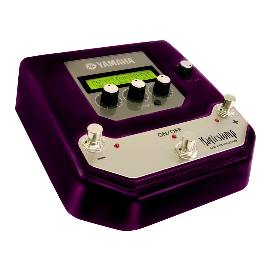
Page 4: Panel Layout
UB99 PANEL LAYOUT (パネルレイアウト) Top Panel (トップパネル) q Display (ディスプレイ) w CONTROL Knobs (コントロールツマミ) e VOLUME Knob (ボリュームツマミ) r STORE Button (ストアボタン) t -Switch, + Switch, ON/OFF Switch (−スイッチ , +スイッチ ,ON/OFF スイッチ) (リアパネル) Rear Panel y INPUT Jack (インプット端子) u INPUT LEVEL HIGH/LOW Switch (インプットレベル切替スイッチ)... - Page 5 IC102 (8P) JK102 IC104 IC105 (8P) IC101 (8P) IC106 (8P) (28P) JK101 IC103 (8P) IC3 (5P) JK103 13,14 SYSTEM RESET IC1 (48P) IC2 (28P) 55,65 IC10 (44P) (176P) IC6 (44P) 12,13 66,67 IC4 (100P) IC7 (64P) AC-10 TR105,106 IC111 IC109 IC108 JK104 IC112...
-
Page 6: Circuit Board Layout
UB99 (ユニットレイアウト) CIRCUIT BOARD LAYOUT Bottom view (分解手順) DISASSEMBLY PROCEDURE Bottom Case ボトムケース (所要時間: 約 1 分) (Time required: About 1 minute) 1-1. [40]のネジ4本と[30]のネジ2本を外し、 ボトムケー 1-1. Remove the four (4) screws marked [40] and the スを外します。 (図 1) two (2) screws marked [30]. The bottom case can then be removed. - Page 7 UB99 Rear Panel リアパネル (Time required: About 3 minutes) (所要時間: 約 3 分) 2-1. Remove the bottom case. (See Procedure 1.) 2-1. ボトムケースを外します。 (1 項参照) (Fig. 2) 2-2. リアパネル面より[110]のネジ 2 本と[120]の特殊六 2-2. Remove the two (2) screws marked [110], the three 角ナット...
-
Page 8: Lsi Pin Description
UB99 (LSI 端子機能表) LSI PIN DESCRIPTION HD6413008VF25 (X4196A00) CPU (MAIN) DM: IC4 NAME FUNCTION NAME FUNCTION Analog power supply +3.3V Port 2 / Address bus /TMO /TMIO Chip select / / / Port B /TMO Port 5 / Address bus /TMIO Ground Data transmission / Port B /WAIT... - Page 9 UB99 M38K07M4L-303HP (X3921200) CPU (USB) DM: IC7 NAME FUNCTION NAME FUNCTION Port P2 (In/output) /INT Port P5 (In/output)/Interruption input Port P1 (In/output) /CNTR Port P5 (In/output)/ /INT Port P5 (In/output)/Interruption input Chip active RESET System reset input Port P5 (In/output) Analog power supply +3.3V Reference voltage input Ground...
- Page 10 UB99 YSS910-S (XV988A00) DSP6 (Digital Signal Processor) DM: IC5 NAME FUNCTION NAME FUNCTION Power supply (3.3 V) Ground Ground DB13 System master clock input (60 MHz or 30 MHz) DB14 System master clock output (High or 30 MHz) DB15 Vdd5 Power supply (5 V) DB16 /SYNCI...
-
Page 11: Ic Block Diagram
UB99 (IC ブロック図) IC BLOCK DIAGRAM (X3936A00) (X3693A00) SN74LVU04APWR SN74LV245APWR Hex Inverter Octal 3-State Bus Transceiver DM: IC107 DM: IC8,9 (X3935A00) SN74LV4040APWR 12-Bit Asynchronous Binary Counter DM: IC110 (XC458A00) (XC011A00) NJM072M NJM5532M (XV423A00) TL072CPSR Dual Operational Amplifier Dual Operational Amplifier DM: IC102,103,105,106 DM: IC101 +DC Voltage... -
Page 12: Circuit Board
UB99 (シート基板図) CIRCUIT BOARD DM Circuit Board OUTPUT INPUT L / MONO INPUT LEVEL AC IN HIGH / LOW Component side ( 部品側) Note: See parts list for details of circuit board component parts. CNA-WC10200-2 注:シートの部品詳細はパーツリストをご参照ください。... - Page 13 UB99 DM Circuit Board VOLUME CONTROL 1 CONTROL 2 CONTROL 3 STORE ON/OFF ON/OFF Pattern side (パターン側) CNA-WC10200-3...
- Page 14 UB99 INSPECTIONS / FACTORY SET 1. Preparation 3-1-1. DSP & DRAM & AD/DA Check 1) Measuring instrument: Oscillator Push [ON/OFF] SW. The following display appears. Distortion meter U B99 DSP&DRAM Level meter PUSH [ON/OFF] 2) Jig: USB cable, P.C (Personal computer) 3) Connections of terminals are shown as follows: Make sure that a signal wave is outputted.
- Page 15 UB99 3-1-3. SRAM Check 3-1-8. SW&LED Check Push [ON/OFF] SW. The following display appears. Push [+] SW. The following display appears. UB99 SRAM CHECK UB99 SW&LED CHECK N OW WRITE & READ PUSH [STORE] SW In a short time, the display is changed as follows. Then, LED (+) will be turned on.
- Page 16 UB99 3-1-13. VR Check 3-1-19. VR Check Turn VR1 (Control 1) slightly clockwise. The following Turn VR3 (Control 3) slightly clockwise. The following display appears. display appears. UB99 VOL2 CHECK UB99 VOL3 CHECK MAX ** [**] ** OK PUSH [ONOFF] SW 3-1-14.
- Page 17 UB99 5. Opening MODE 3-1-25. END Push [ON/OFF] SW. The following display appears. In this mode, the following display appears. MAGICSTOMP UB99 DIAG ALL OK V1.01 PLEASE POWER OFF Turn off power, and the inspection is now completed. Then, the display is changed as follows. Finally, perform "4.
- Page 18 UB99 検査/ファクトリーセット 準備 3-1-1. DSP & DRAM & AD/DA Check 1) 測定器: 発振器 ・[ON/OFF] SW を押します。 歪率計 UB99 DSP&DRAM レベル計 PUSH [ON/OFF] SW 2) 治具:USBケーブル、 P.C. ( パーソナルコンピュータ) 3) 以下に各端子の接続を示します。 と表示され、信号波形が出力されるのを確認します。 INPUT モノラル入力(Signal Input) 3-1-2. 電気的特性 OUT L/ モノラル出力(RL 47K Ω) 項目 入力端子、条件 出力端子、規格値 MONO 1, 入力感度 INPUT OUT L/MONO -4.5dBm(1KHz) 0dBm ± 3dB OUT R モノラル出力(RL 47K Ω)...
- Page 19 UB99 3-1-3. SRAM Check 3-1-8. SW&LED Check ・[ON/OFF] SW を押します。 ・[+] SW を押します。 UB99 SRAM CHECK UB99 SW&LED CHECK NOW WRITE & READ PUSH [STORE] SW と表示し、しばらくすると と表示され LED (+) が点灯します。 UB99 SRAM CHECK 3-1-9. SW&LED Check OK PUSH [ONOFF] SW ・[STORE] SW を押します。 UB99 SW&LED CHECK と表示されます。OK 表示を確認してください。 OK PUSH [ONOFF] SW 3-1-4. FLASH ROM Check ・[ON/OFF] SW を押します。 と表示され LED (―) , LED (ON/OFF) , LED (+) が 3 個点灯します。 UB99 FLASH ROM OK 表示を確認してください。 NOW WRITE & READ 3-1-10. VR Check と表示し、しばらくすると...
- Page 20 UB99 3-1-13. VR Check 3-1-19. VR Check ・VR1 (Control 1) を右に少し回します。 ・VR3(Control 3)を右に少し回します。 UB99 VOL2 CHECK UB99 VOL3 CHECK MAX ** [**] ** OK PUSH [ONOFF] SW と表示されます。 と表示されます。 OK 表示を確認してください。 3-1-14. VR Check ・VR2 (Control 2) を右にいっぱいまで回します。 3-1-20. USB Check ・[ON/OFF]SW を押します。 UB99 VOL2 CHECK UB99 USB CHECK MIN ** [ff ] ** V10103 CNECT USB と表示されます。 と表示されます。 3-1-15. VR Check ・VR2 (Control 2) を左にいっぱいまで回します。 3-1-21. USB Check ・USB Cable で P.C. と接続します。 UB99 VOL2 CHECK UP ** [00] ** UB99 USB CHECK DISCONNECT CABLE と表示されます。 と表示されます。...
- Page 21 UB99 3-1-25. END その後5、Opening 表示をし通常動作となります。 ・ [ON/OFF]SW を押します。 ・Cancel の時は UB99 DIAG ALL OK FACTORY SET PLEASE POWER OFF CANCELLED! と表示されます。 電源を OFF にします。 と表示されます。 これで検査は終了となります。 Opening MODE 最後に 4、Factory Set を行ないます。 MAGICSTOMP V1.01 Factory Set MODE ファクトリーセットを実行すると保存したユーザー パッチ内容はすべて消えてしまいます。 必要なデータ と表示され はセッティングをメモしたり、 コンピューターに保存 してください。 (P.22 参照) WAIT A MOMENT・・・ ・[ON/OFF] SW と[STORE] SW を押しながら電源を ON にします。 と変わり...
- Page 22 UB99 (ユーザーパッチのバックアップ) BACKUP THE USER PATCH DATA 1. Using the supplied USB cable, connect the computer to 1. MAGICSTOMP とコンピューターを付属のUSBケーブ the MAGICSTOMP, then turn on the computer and the ルで接続し、 コンピューターとMAGICSTOMP の電源 MAGICSTOMP. を入れます。 2. Insert the accompanying CD-ROM into your computer. 2.
-
Page 23: Error Messages
UB99 ERROR MESSAGES One of the following messages may appear in the MAGICSTOMP’s display if an error occurs during operation. If so, please stop operation and check the following points to find a solution to the problem. The data being bulk transmitted is damaged. After restoring (overwrite, store, etc.) the user patch data that corresponds to the patch number, try transmitting the data again. -
Page 24: Parts List
GUITAR EFFECTS PROCESSOR UB99 PARTS LIST (目次) CONTENTS (総組立) OVERALL ASSEMBLY ..........2 (トップケースAss'y) TOP CASE ASSEMBLY ......3 (電気部品) ELECTRICAL PARTS ......... 4~8 Notes : DESTINATION ABBREVIATIONS A : Australian model M : South African model B : British model O : Chinese model C : Canadian model Q : South-east Asia model... -
Page 25: Overall Assembly
UB99 (総組立) OVERALL ASSEMBLY Top case assembly: See page 3. (トップケースAss'y) AC Output Power Adaptor AC-10 (J) ( 本品は AC 出力の電源アダプターです。 ) 部 品 名 PART NO. DESCRIPTION REMARKS REF NO. RANK 総 組 立 OVERALL ASSEMBLY UB99 (WB84470) ト ッ プ ケ ー ス A s s y... -
Page 26: Top Case Assembly
UB99 (トップケース Ass'y) TOP CASE ASSEMBLY 部 品 名 PART NO. DESCRIPTION REMARKS REF NO. RANK TOP CASE ASSEMBLY ト ッ プ ケ ー ス A s s y UB99 (WB84480) ト ッ プ ケ ー ス WB842400 Top Case パ... -
Page 27: Electrical Parts
UB99 (電気部品) ELECTRICAL PARTS PART NO. DESCRIPTION 部 品 名 REMARKS REF NO. RANK 電 気 部 品 ELECTRICAL PARTS UB99 D M シ ー ト WC102000 Circuit Board (X3924B0) WC102000 Circuit Board D M シ ー ト (X3924B0) WB843600 Spacer Support PINGOOD MCD2-5 ス... - Page 28 UB99 PART NO. DESCRIPTION 部 品 名 REMARKS REF NO. RANK ケ ミ コ ン C0144 UR847100 Electrolytic Cap. 10.00 25.0V ケ ミ コ ン C0145 UR847100 Electrolytic Cap. 10.00 25.0V C0146 US145100 Ceramic Capacitor-F (chip) 0.1000 25V Z チ ッ プ セ ラ ( F ) -0148 US145100 Ceramic Capacitor-F (chip)
- Page 29 UB99 PART NO. DESCRIPTION 部 品 名 REMARKS REF NO. RANK ホ ー ン ジ ャ ッ ク JK101 V 3 6 3 3 4 0 0 Phone Jack HTJ-064-12I INPUT ホ ー ン ジ ャ ッ ク JK102 V 6 1 7 7 7 0 0 Phone Jack STEREO HTJ-064-12D OUTPUT R...
- Page 30 UB99 PART NO. DESCRIPTION 部 品 名 REMARKS REF NO. RANK チ ッ プ 抵 抗 R0120 RD356470 Carbon Resistor (chip) 4.7K 63M J R0121 RD355330 Carbon Resistor (chip) 330.0 63M J チ ッ プ 抵 抗 R0122 RD355330 Carbon Resistor (chip) 330.0 63M J チ...
- Page 31 UB99 PART NO. DESCRIPTION 部 品 名 REMARKS REF NO. RANK ロ ー タ リ ー V R VR002 WB445700 Rotary Variable Resistor RD09L1140 10KB CONTROL 2 ロ ー タ リ ー V R VR003 WB445700 Rotary Variable Resistor RD09L1140 10KB CONTROL 3 VR101 WB446200...
- Page 32 UB99 DM CIRCUIT DIAGRAM 1/2 UB99 TRANSCEIVER FLASH ROM 16M SRAM 256K STORE PROGRAM SYSTEM RESET ON / OFF CPU (MAIN) to Page 1: G4 to Page 2: H3 TRANSCEIVER from Page 1: D3 from Page 2: H3 CPU (USB) ON / OFF from Page 2: C5 from Page 2: F5...
- Page 33 UB99 DM CIRCUIT DIAGRAM 2/2 UB99 OP AMP INPUT LEVEL OUTPUT R OP AMP INPUT VOLUME OP AMP OP AMP OP AMP from Page 1: D3 OUTPUT L/MONO OP AMP ADC/DAC OP AMP OP AMP OP AMP µPC29M33T-E1(XU965A00) OP AMP NJM7815FA(XD853A00) NJM78M05DLA(XS534A00) REGULATOR +5V...
Need help?
Do you have a question about the Magicstomp UB99 and is the answer not in the manual?
Questions and answers