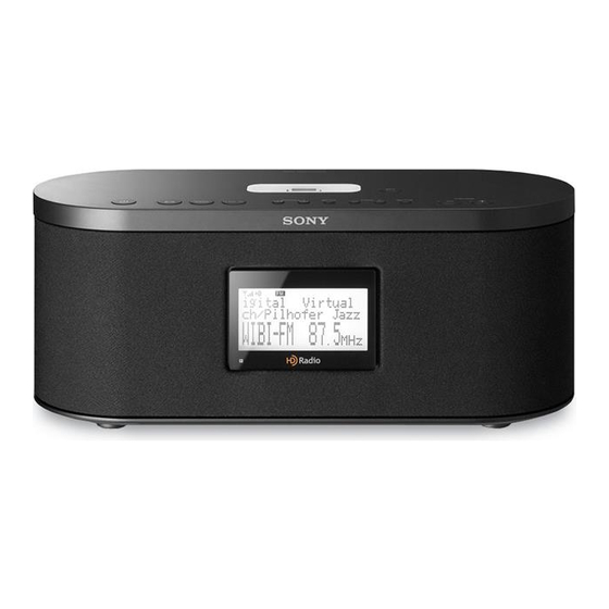
Sony XDR-S10HDiP Service Manual
Hide thumbs
Also See for XDR-S10HDiP:
- Operating instructions (2 pages) ,
- Operating instructions (5 pages) ,
- Operating instructions (2 pages)
Table of Contents
Advertisement
SERVICE MANUAL
Ver. 1.0 2008.05
HD Radio Broadcasting was approved by the Federal Communications
Commission in October 2002 as the system for digital AM and FM
broadcasting in the U.S.
HD Radio technology features include:
– Static-free, clear radio reception.
– FM Multicasting – the ability to broadcast multiple program streams
over a single FM frequency.
– A variety of "data services," including text-based information – artist
name, song title, etc. scrolled across your receiver display.
– Digital broadcasts in the same frequencies as analog broadcasts;
listeners do not need to learn a new station number and today's
stations remain at their current place on the dial.
HD Radio technology is developed and licensed by iBiquity Digital
Corporation and supported by the leaders of the broadcasting, consumer
electronics and automotive industries.
TM
HD Radio
Technology Manufactured Under License From iBiquity
Digital Corporation. iBiquity Digital, the HD Radio logo, and the
HD logo are registered trademarks of iBiquity Digital Corporation.
TM
HD Radio
is a trademark of iBiquity Digital Corporation. U.S. and
Foreign Patents.
9-889-162-01
2008E04-1
XDR-S10HDiP
Time display
12-hour system
Frequency range
Band
Frequency
FM
87.5 – 108 MHz
AM
530 – 1 710 kHz
Speaker
Approx. 6.6 cm (2 5/8 inches) dia. 8 Ω
Input
AUDIO IN jack (ø 3.5 mm stereo minijack)
Antenna terminal
75 Ω antenna terminal for FM
Antenna terminal for AM
Audio power specifi cations
POWER OUTPUT AND TOTAL HARMONIC DISTORTION
With 8-ohm loads, both channels driven from 150-10,000 kHz; rated
3W per channel-minimum RMS, with no more than 10% total harmonic
distortion.
Power output
4 W + 4 W (maximum power)
Power requirements
120 V AC, 60 Hz
Dimensions
Approx. 330 × 130 × 135 mm (w/h/d)
(13 × 5
× 5
1/8
3/8
Mass
Approx. 3.1 kg (6 lb 13.3 oz) incl. power supply unit
Supplied accessories
Remote commander (1)
FM wire antenna (1)
FM dipole antenna (1)
AM loop antenna (1)
Audio connecting cable (1)
Universal dock adapter for iPhone (1)
Connector cover (1)
Design and specifi cations are subject to change without notice.
US Model
SPECIFICATIONS
Channel step
0.1 MHz
10 kHz
inches) not incl. projecting parts and controls
FM/AM DIGITAL RADIO
Advertisement
Table of Contents

Related Manuals for Sony XDR-S10HDiP


Summary of Contents for Sony XDR-S10HDiP
- Page 1 XDR-S10HDiP SERVICE MANUAL US Model Ver. 1.0 2008.05 HD Radio Broadcasting was approved by the Federal Communications SPECIFICATIONS Commission in October 2002 as the system for digital AM and FM Time display broadcasting in the U.S. 12-hour system Frequency range...
- Page 2 COMPONENTS IDENTIFIED BY MARK 0 OR DOTTED LINE WITH MARK 0 ON THE SCHEMATIC DIAGRAMS AND IN THE PARTS LIST ARE CRITICAL TO SAFE OPERATION. REPLACE THESE COMPONENTS WITH SONY PARTS WHOSE PART NUMBERS APPEAR AS SHOWN IN THIS MANUAL OR IN SUPPLEMENTS PUBLISHED BY SONY.
-
Page 3: Table Of Contents
XDR-S10HDiP TABLE OF CONTENTS GENERAL ..............DISASSEMBLY 2-1. Cabinet (Rear) Section ............ 2-2. Wires ................2-3. Chassis Assy ..............2-4. Cabinet (Upper) Section ..........10 2-5. SP101, SP201 ..............10 2-6. MICON Board ..............11 2-7. MAIN Board ..............11 2-8. -
Page 4: General
XDR-S10HDiP SECTION 1 GENERAL This section is extracted from instruction manual. Size AAA (R03) × 2 iPod and VOLUME + buttons have a tactile dot. AC power cord Preparing the remote commander Tag indicator Installing the batteries into the remote commander (See Fig. - Page 5 Apple Inc., registered in supplied audio connecting cable. the U.S. and other countries. Sony cannot accept responsibility in the event iTunes is a registered trademark of Apple Inc. that data recorded on an iPod is lost or...
- Page 6 XDR-S10HDiP To change the sleep timer setting Select “Yes” or “No, ” then press ENTER. to select “ON, ” then press Using iTunes Tagging You can press SLEEP on the remote commander Yes: Deletes all the retrieved data. ENTER. repeatedly to select the desired sleep timer setting No: Cancels the delete operation and ends this “ALARM”...
- Page 7 XDR-S10HDiP Notes on radio reception Connecting the Keep away digital music player or mobile phone from the AM loop antenna or the FM antenna, antenna as this may lead to interference of reception. When you are listening to the radio with an...
-
Page 8: Disassembly
XDR-S10HDiP SECTION 2 DISASSEMBLY • This set can be disassembled in the order shown below. 2-1. CABINET (REAR) SECTION (Page 8) 2-2. WIRES (Page 9) 2-3. CHASSIS ASSY (Page 9) 2-6. MICON BOARD 2-4. CABINET (UPPER) SECTION 2-5. SP101, SP201... -
Page 9: Wires
XDR-S10HDiP 2-2. WIRES POWER board from speaker (L-ch) from speaker (R-ch) 2-3. CHASSIS ASSY CN311 (4P) speaker coard (L-ch) wire (flat type)(11 core) (CN601) speaker coard (R-ch) CN405 (5P) two screws (+P tapping (B2.6)) six screws (+BV tapping (B3)) chassis assy... -
Page 10: Cabinet (Upper) Section
XDR-S10HDiP 2-4. CABINET (UPPER) SECTION two claws cabinet (upper) section three screws (+BV tapping (B3)) two screws (+P tapping (B2.6)) cabinet (front) section two screws (+P tapping (B2.6)) 2-5. SP101, SP201 two screws (+BV tapping (B3)) two screws (+BV tapping (B3)) -
Page 11: Micon Board
XDR-S10HDiP 2-6. MICON BOARD two claws MICON board Remove the thirteen solders. Remove the eleven solders. two screws (+P tapping (B2.6)) 2-7. MAIN BOARD MAIN board two screws (+P tapping (B2.6)) Remove the fourteen solders. -
Page 12: Power Board
XDR-S10HDiP 2-8. POWER BOARD two screws (+P tapping (B2.6)) chassis (MICRO COM PC board) two screws (+P tapping (B2.6)) screw POWER board (+P tapping (B2.6)) Remove the three solders. black green black with line chassis power cord 2-9. ASSEMBLY OF THE POWER CORD When assembly the set, route the power cord as shown below and install it. -
Page 13: Diagrams
XDR-S10HDiP SECTION 3 DIAGRAMS 3-1. BLOCK DIAGRAM PRE AMP IC310 J301 R-CH IN_L3 POWER AMP AUDIO IN IC311 +LOUT DSP TUNER UNIT SP101 L-IN L_OUT BASS SPEAKER (L-CH) –LOUT IN_L1 AUDIO_L BEEP MIX LOGIC 1 FM ANT AUDIO_R R-CH IN_L2... - Page 14 XDR-S10HDiP • Circuit Boards Location THIS NOTE IS COMMON FOR PRINTED WIRING BOARDS AND SCHEMATIC DIAGRAMS. (In addition to this, the necessary note is printed in each block.) For Printed Wiring Boards. For Schematic Diagrams. FAN CONNECTING board Note: Note: IP DOCK board •...
-
Page 15: Printed Wiring Board -Main (Side A) Section
XDR-S10HDiP 3-2. PRINTED WIRING BOARD – MAIN (Side A) Section – • See page 14 for Circuit Boards Location. • : Uses unleaded solder. MAIN BOARD (SIDE A) CN302 1-877-221- (11) IP DOCK BOARD CN601 (Page 18) XDR-S10HDiP... -
Page 16: Printed Wiring Board -Main (Side B) Section
XDR-S10HDiP 3-3. PRINTED WIRING BOARD – MAIN (Side B) Section – • See page 14 for Circuit Boards Location. • : Uses unleaded solder. MAIN BOARD (SIDE B) • Semiconductor Location Ref. No. Location D950 D951 D952 C964 D953 D990... -
Page 17: Schematic Diagram -Main Section
XDR-S10HDiP 3-4. SCHEMATIC DIAGRAM – MAIN Section – • See page 27 for IC Block Diagrams. CN901 D950 IC955 IC950 IC B/D IC B/D IC B/D (Page 26) C950 C955 R961 R950 R956 Q954 Q950 R953 R962 R959 R951 R954... -
Page 18: Printed Wiring Board -Ip Dock Section
XDR-S10HDiP 3-5. PRINTED WIRING BOARD – IP DOCK Section – • See page 14 for Circuit Boards Location. • : Uses unleaded solder. IP DOCK BOARD (SIDE A) IP DOCK BOARD (SIDE B) R611 C607 R612 R609 R613 R610 R608... -
Page 19: Schematic Diagram -Ip Dock Section
XDR-S10HDiP 3-6. SCHEMATIC DIAGRAM – IP DOCK Section – CN602 R615 R614 R612 R613 C607 R611 R610 FB608 R608 FB609 R609 FB606 CN601 FB607 FB604 C602 FB605 C601 R601 (Page 17) FB602 FB603 FB601 XDR-S10HDiP... -
Page 20: Printed Wiring Board -Micon (Side A) Section
XDR-S10HDiP 3-7. PRINTED WIRING BOARD – MICON (Side A) Section – • See page 14 for Circuit Boards Location. • : Uses unleaded solder. MICON BOARD (SIDE A) KEY (MAIN) BOARD W701 (Page 22) MAIN BOARD CN402 (Page 16) CN401... -
Page 21: Printed Wiring Board -Micon (Side B) Section
XDR-S10HDiP 3-8. PRINTED WIRING BOARD – MICON (Side B) Section – • See page 14 for Circuit Boards Location. • : Uses unleaded solder. MICON BOARD • Semiconductor (SIDE B) Location Ref. No. Location D401 D402 B-12 D401 D402 D403... -
Page 22: Printed Wiring Boards -Key Section
XDR-S10HDiP 3-9. PRINTED WIRING BOARDS – KEY Section – • See page 14 for Circuit Boards Location. • : Uses unleaded solder. KEY (MAIN) BOARD — TUNE — PRESET iPod RADIO/ SURROUND POWER BAND AUDIO IN MENU ENTER — VOLUME... -
Page 23: Schematic Diagram -Micon Section
XDR-S10HDiP 3-10. SCHEMATIC DIAGRAM – MICON Section – • See page 14 for waveforms. • See page 28 for IC Block Diagram. • See page 30 for IC Pin Function Description of IC401. IC701 RB417 R816 R815 R813 R809 R808... -
Page 24: Printed Wiring Board -Power (Side A) Section
XDR-S10HDiP 3-11. PRINTED WIRING BOARD – POWER (Side A) Section – • See page 14 for Circuit Boards Location. • : Uses unleaded solder. POWER BOARD (SIDE A) C327 C326 FB314 FB312 FB313 C319 FB318 FB311 C312 C911 C382 1-877-222-... -
Page 25: Printed Wiring Board -Power (Side B) Section
XDR-S10HDiP 3-12. PRINTED WIRING BOARD – POWER (Side B) Section – • See page 14 for Circuit Boards Location. • : Uses unleaded solder. J301 AUDIO IN POWER BOARD (SIDE B) • Semiconductor Location Ref. No. Location FAN CONNECTING D101... -
Page 26: Schematic Diagram -Power Section
XDR-S10HDiP 3-13. SCHEMATIC DIAGRAM – POWER Section – • See page 27 to 29 for IC Block Diagrams. R204 C209 R202 C295 C195 J301 R188 R289 R288 R189 C213 R104 C109 C252 C253 C152 C153 R103 R203 R102 C108 C107 C208... - Page 27 XDR-S10HDiP • IC Block Diagrams IC950 NJM2387ADL3(TE2) (MAIN Board) IC951 NJM2878F4-33(TE2) (MAIN Board) IC952 NJM2387ADL3(TE2) (MAIN Board) IC954 NJM2387ADL3(TE2) (MAIN Board) IC955 NJM2387ADL3(TE2) (MAIN Board) IC990 NJM2387ADL3(TE2) (MAIN Board) VOUT IC980 NJM2387ADL3(TE2) (POWER Board) CONT 1 CURRENT THEMAL LIMIT PROTECTOR...
- Page 28 XDR-S10HDiP IC403 XC61CN2702NR (MICON Board) VREF IC310 BD3870FS-E2 (POWER Board) TREBLE1 TREBLE2 BASS2 BASS1 LOGIC =8kHz =8kHz =80Hz =80Hz VCC/2 VCC/2 VCC/2 VCC/2 VCC/2 11 12 IC380 NJM2746RB1 (POWER Board) AOUT A–IN BOUT B–IN A+IN B+IN...
- Page 29 XDR-S10HDiP IC311 TDA7266P13TR (POWER Board) P-GND 1 P-GND NC 2 NC 3 NC 4 +ROUT 5 –ROUT 6 R-IN +LOUT NC 9 –LOUT Vref MUTE 10 L-IN ST-BY 11 S-GND NC 12 IC901 XC6213B332MR (POWER Board) VIN 1 ON/OFF CONTROL...
- Page 30 XDR-S10HDiP • IC Pin Function Description MICON BOARD IC401 R5F3640MDFAR (SYSTEM CONTROL, LCD DRIVE) Pin No. Pin Name Description SOUT NC — Not used (Open) CLK4 NC — Not used (Open) P9_4 RMT Remote control signal input P9_3 NC —...
- Page 31 XDR-S10HDiP Pin No. Pin Name Description P4_1/NC Not used (Open) P4_0/NC Not used (Open) P3_7/D0 LCD data D0 output P3_6/D1 LCD data D1 output P3_5/D2 LCD data D2 output P3_4/D3 LCD data D3 output P3_3/D4 LCD data D4 output P3_2/D5...
-
Page 32: Exploded Views
XDR-S10HDiP SECTION 4 EXPLODED VIEWS Note: • -XX and -X mean standardized parts, so • Color Indication of Appearance Parts Ex- The components identifi ed by mark 0 they may have some difference from the ample: or dotted line with mark 0 are critical for original one. -
Page 33: Cabinet (Front) Section
XDR-S10HDiP 4-2. CABINET (FRONT) SECTION SP101 chassis section SP201 Ref. No. Part No. Description Remark Ref. No. Part No. Description Remark 3-254-143-11 SCREW (B3), (+) BV TAPPING 4-000-738-01 SHEET (A), ADHESIVE 3-285-549-01 CABINET (FRONT) 3-254-151-01 SCREW (B2.6), (+) P TAPPING... -
Page 34: Cabinet (Upper) Section
XDR-S10HDiP 4-3. CABINET (UPPER) SECTION Ref. No. Part No. Description Remark Ref. No. Part No. Description Remark X-2318-228-1 CABINET (UPPER) SUB ASSY 3-259-210-01 CUSHION (H) A-1547-621-A KEY (TAG) BOARD, COMPLETE A-1547-622-A IP DOCK BOARD, COMPLETE 3-254-151-01 SCREW (B2.6), (+) P TAPPING... -
Page 35: Chassis Section
XDR-S10HDiP 4-4. CHASSIS SECTION not supplied (TU1) IDM1 T901 Ref. No. Part No. Description Remark Ref. No. Part No. Description Remark 3-198-658-01 COVER (DSP01, A) 3-876-441-01 CHASSIS (MICRO COM PC BOARD) 3-198-659-01 COVER (DSP01, B) X-2318-229-1 MICON BOARD, COMPLETE 3-285-558-01... -
Page 36: Electrical Parts List
XDR-S10HDiP SECTION 5 FAN CONNECTING IP DOCK ELECTRICAL PARTS LIST KEY (MAIN) KEY (TAG) Note: • Due to standardization, replacements in • CAPACITORS When indicating parts by reference num- the parts list may be different from the uF: μF ber, please include the board name. - Page 37 XDR-S10HDiP KEY (TAG) MAIN Ref. No. Part No. Description Remark Ref. No. Part No. Description Remark < SWITCH > FB54 1-414-227-11 INDUCTOR, FERRITE BEAD FB55 1-414-227-11 INDUCTOR, FERRITE BEAD S813 1-554-937-11 SWITCH, TACTILE (Tag) FB56 1-414-227-11 INDUCTOR, FERRITE BEAD ************************************************************* <...
- Page 38 XDR-S10HDiP MAIN MICON Ref. No. Part No. Description Remark Ref. No. Part No. Description Remark R954 1-208-855-81 METAL CHIP 0.5% 1/16W C416 1-107-820-11 CERAMIC CHIP 0.1uF R955 1-208-683-11 METAL CHIP 0.5% 1/16W C417 1-164-874-11 CERAMIC CHIP 100PF R956 1-218-973-11 RES-CHIP...
- Page 39 XDR-S10HDiP MICON POWER Ref. No. Part No. Description Remark Ref. No. Part No. Description Remark < DIODE > R472 1-218-985-11 RES-CHIP 470K 1/16W R473 1-218-985-11 RES-CHIP 470K 1/16W D401 6-502-332-01 LED SDPW31H1C0000 (LCD BACK LIGHT) R474 1-218-969-11 RES-CHIP 1/16W D402...
- Page 40 XDR-S10HDiP POWER Ref. No. Part No. Description Remark Ref. No. Part No. Description Remark C117 1-164-870-11 CERAMIC CHIP 68PF C203 1-100-415-11 CERAMIC CHIP 0.47uF 6.3V C118 1-164-854-11 CERAMIC CHIP 15PF C204 1-164-937-11 CERAMIC CHIP 0.001uF C119 1-164-854-11 CERAMIC CHIP 15PF...
- Page 41 XDR-S10HDiP POWER Ref. No. Part No. Description Remark Ref. No. Part No. Description Remark C285 1-164-854-11 CERAMIC CHIP 15PF C379 1-164-870-11 CERAMIC CHIP 68PF C286 1-164-854-11 CERAMIC CHIP 15PF C380 1-164-854-11 CERAMIC CHIP 15PF C287 1-164-870-11 CERAMIC CHIP 68PF C381...
- Page 42 XDR-S10HDiP POWER Ref. No. Part No. Description Remark Ref. No. Part No. Description Remark D917 8-719-988-61 DIODE 1SS355TE-17 R111 1-218-961-11 RES-CHIP 4.7K 1/16W D918 8-719-083-58 DIODE UDZSNPTE-173.9B R115 1-218-953-11 RES-CHIP 1/16W D919 8-719-988-61 DIODE 1SS355TE-17 R116 1-218-973-11 RES-CHIP 1/16W R117...
- Page 43 XDR-S10HDiP POWER Ref. No. Part No. Description Remark R383 1-218-985-11 RES-CHIP 470K 1/16W R384 1-218-973-11 RES-CHIP 1/16W R385 1-218-973-11 RES-CHIP 1/16W R901 1-218-965-11 RES-CHIP 1/16W R902 1-218-961-11 RES-CHIP 4.7K 1/16W R903 1-218-961-11 RES-CHIP 4.7K 1/16W R904 1-218-965-11 RES-CHIP 1/16W R905...
- Page 44 XDR-S10HDiP REVISION HISTORY Checking the version allows you to jump to the revised page. Also, clicking the version at the top of the revised page allows you to jump to the next revised page. Ver. Date Description of Revision 2008.05...
Need help?
Do you have a question about the XDR-S10HDiP and is the answer not in the manual?
Questions and answers