
Related Manuals for Toshiba SD-V55HTSU


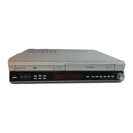
Summary of Contents for Toshiba SD-V55HTSU
- Page 1 FILE NO. 810-200425 CIRCUIT DIAGRAMS DVD/VCR Home Theater System SD-V55HTSU SD-V55HTSC DOCUMENT CREATED IN JAPAN, May, 2004...
-
Page 2: Table Of Contents
SECTION 3 ELECTRICAL CONTENTS OVERALL WIRING DIAGRAM DVD & AMP PART ......3-2 VCR PART ELECTRICAL TROUBLESHOOTING GUIDE ................3-54 ELECTRICAL ADJUSTMENT 1. SYSTEM OPERATION FLOW......3-54 2. TEST & DEBUG FLOW........3-55 PROCEDURES ............3-3 3. AUDIO µ-COM CIRCUIT(DVD & AMP)....3-63 ELECTRICAL TROUBLESHOOTING DETAILS AND WAVEFORMS ON GUIDE ................3-4 SYSTEM TEST AND DEBUGGING... -
Page 3: Overall Wiring Diagram
OVERALL WIRING DIAGRAM... -
Page 4: Vcr Part
VCR PART ELECTRICAL ADJUSTMENT PROCEDURES 1. Servo Adjustment 1) PG Adjustment • Test Equipment a) OSCILLOSCOPE b) NTSC MODEL : NTSC SP TEST TAPE • Adjustment And Specification MODE MEASUREMENT POINT ADJUSTMENT POINT SPECIFICATION V.Out PLAY R/C TRK JIG KEY 6.5 ±... -
Page 5: Electrical Troubleshooting Guide
ELECTRICAL TROUBLESHOOTING GUIDE 1. Power(SMPS) CIRCUIT (1) No 5.3VA (SYS/Hi-Fi/TUNER) (2) No 12VA (TO CAP, DRUM MOTOR) NO 5.3VA. NO 12VA. Replace the F101. Is the Vcc(13V) supplied Check or Replace Is the F101 normal? (Use the same Fuse) to (+) terminal in D126? the D126. - Page 6 (4) No 5V (TO DVD) (5) No 33V (TUNER) NO 5V. No 33V. Is 5.3VA put into Check the Power 5.3VA Line Check. Is Q163 Base “H”? the Q168 Emitter? Control. Is the Q169 Base Check the Power Check or Replace “H”? Control.
-
Page 7: System/Key Circuit
2. SYSTEM/KEY CIRCUIT (1) AUTO STOP Auto Stop Does the SW30 waveform Check the Drum Motor appear at the IC501 signal. Pin18? Do T/UP Reel Pulses Do the T-UP Reel Pulses Does 5V appear at the appear at the point appear at the IC501 Pin80? RS501? between R556 and R536? -
Page 8: Servo Circuit
3. SERVO CIRCUIT (1) Unstable Video in PB MODE Unstable Video in PB Mode. Does the Noise level of the screen change periodically? Do the CTL pulses appear Is adjusting the height of at the IC501 Pin97? the CTL Head accurate? Does the CFG waveform Readjust the height of the appear at the IC501... - Page 9 2. SERVO CIRCUIT (3) When the Capstan Motor doesn’t run, When the Capstan Motor doesn’t run, Refer to “SMPS(CAPSTAN/12Volt) Does 12VA appear at the PMC01? Trouble Shooting”. Is “DRUM CTL” 2.8V appear at the PMC01? Check the PMC01 and the Capstan Does the PWM signal appear at the IC501 Pin77? Motor Ass’y.
-
Page 10: Osd Circuit
2. SERVO CIRCUIT (4) KEY doesn’t working KEY doesn’t working. Is 5V applied to the IC501 Refer to “SMPS 5.3VA Pin2, 3? Trouble Shooting”. Does LED or FLD change Replace the defective when a function button is switches. pressed? 4. OSD CIRCUIT (1) No OSD display. -
Page 11: Y/C Circuit
5. Y/C CIRCUIT (1) No Video in EE Mode, No Video in EE Mode Does the Video signal Does the Video signal Check DVD Video Input appear at the IC301 appear at the IC302 (IC602, Pin4), Tuner Video Pins28, 30, 32? Pins1, 5? Input (TU701 Pin16), Line Video Input (JK601),... - Page 12 3. Y/C CIRCUIT (2) When the Y(Luminance) signal doesn’t appear on the screen in PB Mode, Is 5V applied to the IC301 Check the line of the REG 5V Line. (Power Circuit) Pins23, 44, 45, 52, 68, 77? Is the Y/C Bus siganl Refer to ‘SYSTEM Y/C applied to the IC301 BUS CHECK Trouble...
- Page 13 3. Y/C CIRCUIT (3) When the C(Color) signal doesn’t appear on the screen in PB Mode, Is 5V applied to the IC301 Check the line of the REG 5V Line. (Power Circuit) Pins23, 44, 45, 52, 68, 77? Is normal the X301 Does the fsc signal appear (3.58MHZ) of oscillation Replace the X301.
- Page 14 3. Y/C CIRCUIT (4) When the Video signal doesn’t appear on the screen in REC Mode, REC mode Is EE mode normal? Check the EE mode Is brightness normal? Is color normal? Is the brightness signal sup- Does signal appear at Check X301 oscillation IC301 Pins41, 50? frequency.
-
Page 15: Tuner/If Circuit
6. Tuner/IF CIRCUIT (1) No Picture on the TV screen No picture on the TV screen Does the Video signal at Is +33V applied to TU701 Check 33V line. the TU701 Pin16. Pin14? Is +5V applied to TU701 Check 5V line. Pin3? Does the Clock signal Check the lIC Clock Signal... - Page 16 (2) No Sound No Sound. Check the Vcc of TU701 Pins3, 14. Check 5.2V, 33V Line. Check the Tuner SiF signal at IC801 Check the Tuner SIF of TU701 Pin13. Pin57. 1. Check the Vcc(5.3VA, 9V) of IC801 Check the Audio of IC801 Pins78, 80. Pins3, 5, 36, 54.
-
Page 17: Hi-Fi Circuit
7. Hi-Fi Circuit Hi-Fi Playback. Check the Vcc of IC801. No sound (Pins 3, 15, 32, 46) Check the Hi-Fi Selection Check power. Switch and the Tape quality. Is the RF waveform at IC801 Pin 23 over 3V Vp-p? Is Pin 30 of IC801 over Check REC start “H”... - Page 18 Hi-Fi REC. It is impossible to record and playback Hi-Fi Audio signal. Check Vcc of IC801. (Pins 3, 15, 32, 46) Check IC801 Pin 37(Data),Pin 38(CLOCK). Check Power. Is IC501 Pin 84(A.Mute) “High”? Check ports of µ-COM. Are Audio signals present at IC801 Check the Port of µ-COM.
-
Page 20: Block Diagrams
RECTIFIER & SMOOTHING BLOCK ( D129, C144, L124, C147 ) PW101 FEED-BACK C122 BLOCK ( R132, R133, C148, R134, R135, R136, IC105 R137 ) IC106 (BK) (WH) TOSHIBA SD-V55HTSU/SC NOTES) Symbol denotes AC ground. NOTES) Symbol denotes DC chassis ground. 3-18 3-19... -
Page 21: Power(Smps) Block Diagram 2
(Q167, C168, R175, R176, R177) TO SYS 5.3VA PVS01 TO TU/SYS/ Hi-Fi 5.2V PWR CTL BLOCK FROM µ-COM (Q169, C170, R181, PWR CTL 'H' R182, R183) REG 5V TO AVCP (Q166, C166, C167, REG 5V R174, ZD161) TOSHIBA SD-V55HTSU/SC 3-20 3-21... -
Page 22: Y/C Block Diagram
3.58M MAIN C-LPF VIDEO BPF1 CONV 4.21M 3.58M BPF1 4.21M COMB DETAIL CLAMP CONV COMB LINE2 CLAMP MAIN SP PB 'B' CONV SP REC EMPHA EMPHA SP PB 'A' V.OUT V.OUT DOUBLE FM-EQ MAIN DE-EM FM-EQ TOSHIBA SD-V55HTSU/SC 3-22 3-23... -
Page 23: Normal Audio Block Diagram
4. NORMAL AUDIO BLOCK DIAGRAM 1) EE Mode 2) PB Mode 3) REC Mode TOSHIBA SD-V55HTSU/SC 3-24 3-25... -
Page 24: Hi-Fi Block Diagram
DVD A.IN 'R' AV1 A.IN 'L' INPUT REAR JACK OUTPUT SELECT AV1 A.IN 'R' SELECT MODULATOR AV2 A.IN 'L' A.OUT IC801 FRONT (To Tu) AV2 A.IN 'R' LA72670M NORMAL AUDIO OUT(To AVCP) NORMAL AUDIO IN(From AVCP) TOSHIBA SD-V55HTSU/SC 3-26 3-27... -
Page 25: System Block Diagram
SUP Reel POWER FAIL SUP REEL R558 C582 IC504 CST IN RESET CST.SW/REC TAP Q503 5.3VA C500 5.3VA IC505 R541 R531 CS501 R5C6 R544 Q501 L511 R583 C552 R529 R598 C595 C596 L512 C592 C503 C561 L501 TOSHIBA SD-V55HTSU/SC 3-28 3-29... -
Page 26: Circuit Diagrams
2. Voltages are DC-measured with a digital voltmeter MODIFIED OR ALTERED WITHOUT PERMISSION IMPLEMENTATION OF THE LATEST SAFETY AND during Play mode. FROM THE TOSHIBA ELECTRONICS CORPORATION. PERFORMANCE IMPROVEMENT CHANGES INTO ALL COMPONENTS SHOULD BE REPLACED ONLY THE SET IS NOT DELAYED UNTIL THE NEW SERVICE WITH TYPES IDENTICAL TO THOSE IN THE ORIGI- LITERATURE IS PRINTED. -
Page 27: Power(Smps) Circuit Diagram 2
2. POWER(SMPS) CIRCUIT DIAGRAM 2 3-32 3-33... -
Page 28: Jack/Tuner Circuit Diagram
3. JACK, TUNER CIRCUIT DIAGRAM 3-34 3-35... -
Page 29: A/V Circuit Diagram
4. A/V CIRCUIT DIAGRAM IC301 Pins 53, 54, 55 are defective. IC301 doesn’t operate. X301 is defective. PB COLOR Signal disappear. IC301 Pin 57 is defective. PB COLOR Signal disappear. IC301 Pin 59 is defective. Auto Tracking is failed. Q306, Q307 are defective. EE, PB Screen doesn’t appear. -
Page 30: Hi-Fi Circuit Diagram
5. Hi-Fi CIRCUIT DIAGRAM IC801 Pins37, 38 aredefective. No Audio 23 Pin is defective. No Hi-Fi Audio 3-38 3-39... -
Page 31: System Circuit Diagram
6. SYSTEM CIRCUIT DIAGRAM OSD will not operate. µ-COM will not operate. L511, R598, C595, C596 are defective. OSD is unstable. X501, X502 are defective. R597, C590, C589 are defective. Deck will not operate. R575, R576, R577, R578 are defective. µ-COM is unstable. -
Page 32: Key Circuit Diagram
7. KEY CIRCUIT DIAGRAM 3-42 3-43... -
Page 33: Waveforms
• WAVEFORMS * IC301 Waveform * IC501 Waveform Stop : 10.0KS/s 280 Acqs Stop : 250KS/s 299 Acqs Stop : 10.0KS/s 18 Acqs Trigger Position: 12% Stop : 10.0KS/s 27 Acqs 1.00 V M 5.00ms 3.04 V 1.00 V M5.00ms 3.04 V 1.00 V M 200µs... -
Page 34: Circuit Voltage Chart
• CIRCUIT VOLTAGE CHART MODE MODE MODE MODE MODE MODE Base Emitter Collector Location PLAY PLAY PLAY PLAY PLAY PLAY PIN NO. PIN NO. PIN NO. PIN NO. PIN NO. PIN NO. I C 3 0 1 0.68 0.93 5.19 5.19 3.86 0.23... -
Page 35: Printed Circuit Diagrams
PRINTED CIRCUIT DIAGRAMS 1. MAIN P.C.BOARD LOCATION GUIDE 3-48 3-49... -
Page 36: Power P.c.board
2. POWER P.C.BOARD LOCATION GUIDE 3-50 3-51... -
Page 37: Key 1(Left) P.c.board
3. KEY 1(LEFT) P.C.BOARD LOCATION GUIDE 4. KEY 2(RIGHT) P.C.BOARD LOCATION GUIDE 3-52 3-53... -
Page 38: Dvd & Amp Part
DVD & AMP PART ELECTRICAL TROUBLESHOOTING GUIDE 1. System operation flow Power On 1. 8032 initializes SERVO, DSP & RISC registers 2. Write RISC code to SDRAM 3. Reset RISC Show LOGO Tray Closed? Tray Close to Closed position SLED at Inner Side? SLED Moves to Inner Position Judge whether have disc and disc type... -
Page 39: Test & Debug Flow
2. Test & debug flow TEST Check the AC Vol tage Check the POWER PART Power PCBA (110V or 220V) Switch on the Power PCBA the DC Voltage outputs OK? Check the POWER PART (5V, 3.3V, 8V, 12V) Is 3.3V and 2.5V DC Check the regulators or diode(D501). - Page 40 RESET or Power On. Flash Check connection lines between FLASH Memory operates Show LOGO? & MT1379 and the FLASH access time properly? whether is suitable or not. SDRAM Check connection lines between SDRAM(IC502,IC503) & MT1379 and the works properl y? SDRAM is damaged.
- Page 41 Does the SLED move Check the connection line of Motor Driver STBY to inner side when it is at STBY signal . Pin is High? outer position? Check the related circuit of Motor Driver STBY FMSO. Pin is High? Check the amp circuit on SL+ and SL- output motor driver.
- Page 42 Check the laser power circuit Laser turns on when LD01 or LD02 output on MT1336 and connecting to reading disc? properly? power transistor. (Q404, Q405) Collector Check the related circuit on voltage of power transistor is OK? laser power transistor (Q404, Q405) Check cable connection between transistor output and pick-up head.
- Page 43 Proper Check connections between signals on A, B, C, Focus ON OK? MT1336 and pick-up head. D of MT1336 Check the related circuit Proper FEO signal on MT1336 FEO signal . on MT1336? Check FEO connection between MT1336 and MT1379 Check the related Proper FEO signal Track On OK?
- Page 44 Audio Normal DAC received Check connection between MT1379 Audio output & Audio DAC. (Check ARCK, ALRCK correct data stream? when disc playback? ACKL, ASDAT3) Normal Check the related circuit of Audio DAC Audio DAC. (Check Audio out? (IC206) out Pins 8, 5) Check Audio filter, amplify, mute circuit.
-
Page 45: Audio Μ-Com Circuit(Dvd & Amp)
3. AUDIO µ-COM Circuit(DVD & AMP) POWER ON Does CD/DVD appear Does CD/DVD appear at FLT? at FLT? Does Loading appear Does it appear DVD Error at FLD? at FLD? Does no Dise or Time Check Connector (DVV01) Reconnet it. appear at FLD? if is normally. -
Page 46: Details And Waveforms On System Test And Debugging
DETAILS AND WAVEFORMS ON SYSTEM TEST AND DEBUGGING 1. SYSTEM 27MHz CLOCK,RESET,FLASH R/W SIGNAL 1) MT1379 main clock is at 27MHz(X501) 3.8V, 27MHz FIG 1-1 2) MT1379 & MT1336 reset is high active. Power Cord in 5.2VA PWR_CTL(SYSTEM µ-COM) IC501 PIN83) M_RESET(PDV03 PIN6) URST(IC501 PIN 188) FIG 1-2... - Page 47 3) RS232 waveform during procedure(Downloading) TXD(J501 PIN3) RXD(J501 PIN 2) FIG 1-3 4) Flash R/W enable signal during download(Downloading) FRD(IC5A1 PIN 28) FWR(IC5A1 PIN 11) FIG 1-4 3-63...
-
Page 48: Sdram Clock
2. SDRAM CLOCK 1) MT1379 main clock is at 27MHz(X501) DCLK = 93MHz, Vp-p=2.2, Vmax=2.7V (IC502,IC503 PIN 35) FIG 2-1 3. TRAY OPEN/CLOSE SIGNAL 1) Tray open/close waveform OPEN((PDM03 PIN7) CLOSE(PDM03 PIN8) TROPEN(IC402 PIN 1) TRCLOSE(IC402 PIN 2) FIG 3-1 3-64... - Page 49 2) Tray close waveform OPEN((PDM03 PIN7) CLOSE(PDM03 PIN8) TROPEN(IC402 PIN 1) TRCLOSE(IC402 PIN 2) FIG 3-2 3) Tray open waveform OPEN(PDM03 PIN7) CLOSE(PDM03 PIN8) TROPEN(IC402 PIN 1) TRCLOSE(IC402 PIN 2) FIG 3-3 3-65...
-
Page 50: Sled Control Related Signal (No Disc Condition)
4. SLED CONTROL RELATED SIGNAL (NO DISC CONDITION) FMSO(2.0V/1.4V/1.0V) (IC501 PIN 19) STBY(5V) – (IC401 PIN 50) SL+(4.7V/3.6V/1.9V) (IC402 PIN 12) SL-(5.3V/3.7V/2.5V) (IC402 PIN 13) FIG 4-1 5. LENS CONTROL RELATED SIGNAL(NO DISC CONDITION) FOSO(1.5V/1.4V/1.3V) (IC501 PIN 12) F+(4.0V/3.6V/3.2V) (IC402 PIN 9) F-(4.0V/3.6V/3.2V) (IC402 PIN 8) FIG 5-1... -
Page 51: Laser Power Control Related Signal(No Disc Condition)
6. LASER POWER CONTROL RELATED SIGNAL(NO DISC CONDITION) MDI1(0V/180mV) (IC401 PIN 124) LD01(5.0V//3.5V) IC401 PIN 125) LD02(5.0V/3.6V) (IC401 PIN 126) FIG 6-1 7. DISC TYPE JUDGEMENT WAVEFORMS F+(IC402 PIN 9) FE(IC401 PIN 18) RFL(IC401 PIN 19) FIG 7-1 (DVD) 3-67... - Page 52 F+(IC402 PIN 9) FE(IC401 PIN 18) RFL(IC401 PIN 19) FIG 7-2 (DVD) F+(IC402 PIN 9) FE(IC401 PIN 18) RFL(IC401 PIN 19) FIG 7-3 (CD) 3-68...
-
Page 53: Focus On Waveforms
F+(IC402 PIN 9) FE(IC401 PIN 18) RFL(IC401 PIN 19) FIG 7-4 (CD) 8. FOCUS ON WAVEFORMS FE(IC401 PIN 18) FOSO(IC501 PIN12) F+(IC402 PIN 9) F-(IC402 PIN 8) FIG 8-1 (DVD) 3-69... -
Page 54: Spindle Control Waveforms (No Disc Condition)
FE(IC401 PIN 18) FOSO(IC501 PIN12) F+(IC402 PIN 9) F-(IC402 PIN 8) FIG 8-2 (CD) 9. SPINDLE CONTROL WAVEFORMS (NO DISC CONDITION) DMSO(1.4V/1.8V) (IC501 PIN 18) SP-(3.6V/2.4V) (IC402 PIN 10) SP+(3.6V/4.8V) (IC402 PIN 11) FIG 9-1 3-70... -
Page 55: Tracking Control Related Signal(System Checking)
10. TRACKING CONTROL RELATED SIGNAL(System checking) TE(IC401 PIN 21) TRSO(IC501 PIN 13) T-(IC402 PIN 7) T+(IC402 PIN 6) FIG 10-1(DVD) TE(IC401 PIN 21) TRSO(IC501 PIN 13) T-(IC402 PIN 7) T+(IC402 PIN 6) FIG 10-2(CD) 3-71... -
Page 56: Rf Waveform
11. RF WAVEFORM RFOP(2.3V/1.1V) (IC401 PIN 6) RFON(0.8V/2.0V) (IC401 PIN 7) FIG 11-1 12. MT1379 VIDEO OUTPUT WAVEFORMS 1) Full colorbar signal(CVBS) (IC507 PIN 23) FIG 12-1 3-72... - Page 57 2) Y (IC507 PIN 21) FIG 12-2 3) C (IC507 PIN 26) FIG 12-3 3-73...
-
Page 58: Audio Output From Audio Dac
13. AUDIO OUTPUT FROM AUDIO DAC 1) Audio L/R (IC206 PIN 8,5) FIG 13-1 2) Audio related Signal ASDATA3 ASDAT3(IC501 PIN 157) ABCK(IC501 PIN 148) ALRCK(IC501 PIN 149) FIG 13-2 3-74... -
Page 59: Dvd & Amp Waveforms
14. DVD & AMP WAVEFORMS • R311 → FRONT L • R303 → FRONT R • R309 → SURROUND L • R301 → SURROUND R • R307 → CENTER • R305 → WOOFER 3-75... -
Page 60: Block Diagrams
BLOCK DIAGRAMS 1. Overall Block Diagram Y[1:6] MA11,BA1 DQM[0:1] CVBS DQ[00:15] ASPECT DVD_DATA_OUT DVD_ESET F+,F-,T+,T- SP+,SP- SL+,SL- LOAD+,LOAD- DECK MECHANISM TOSHIBA SD-V55HTSU/SC 3-76... -
Page 61: Servo Block Diagram
2. SERVO Block Diagram TOSHIBA SD-V55HTSU/SC 3-77... -
Page 62: Mpeg & Memory Block Diagram
3. MPEG & MEMORY Block Diagram TOSHIBA SD-V55HTSU/SC 3-78... -
Page 63: Video & Audio Block Diagram
4. VIDEO & AUDIO Block Diagram TOSHIBA SD-V55HTSU/SC 3-79... -
Page 64: Dvd & Amp Block Diagram
5. DVD & AMP Block Diagram TOSHIBA SD-V55HTSU/SC 3-80... -
Page 66: Circuit Diagrams
CIRCUIT DIAGRAMS 1. MPEG CIRCUIT DIAGRAM No Video signal No Power on System not working or screen is abnormal Incomplete Digitron Video signal Y System not working Video signal Color 3-81 3-82... -
Page 67: Rf & Servo Circuit Diagram
2. RF & SERVO CIRCUIT DIAGRAM 3-83 3-84... -
Page 68: Audio, Μ-Com Circuit Diagram(Dvd & Amp)
3. AUDIO, µ_COM CIRCUIT DIAGRAM(DVD & AMP) TUNER_L TUNER_R 3-85 3-86... -
Page 69: Digital Amp Circuit Diagram (Dvd & Amp)
4. DIGITAL AMP CIRCUIT DIAGRAM (DVD & AMP) 3-87 3-88... -
Page 70: Pwm & Codeic Circuit Diagram (Dvd & Amp)
5. PWM & CODEIC CIRCUIT DIAGRAM (DVD & AMP) 3-89 3-90... -
Page 71: Interface Circuit Diagram (Dvd & Amp)
6. INTERFACE CIRCUIT DIAGRAM (DVD & AMP) 3-91 3-92... -
Page 72: Circuit Voltage Chart
• CIRCUIT VOLTAGE CHART MODE MODE MODE MODE MODE MODE MODE MODE MODE MODE STOP PLAY STOP PLAY STOP PLAY STOP PLAY STOP PLAY STOP PLAY STOP PLAY STOP PLAY STOP PLAY STOP PLAY PIN NO. PIN NO. PIN NO. PIN NO. - Page 73 MODE MODE MODE MODE MODE STOP PLAY STOP PLAY STOP PLAY STOP PLAY STOP PLAY STOP PLAY SECTION PIN NO. PIN NO. PIN NO. PIN NO. PIN NO. 0.59 3.28 3.29 2.83 3.12 15.61 15.61 3.24 3.23 DVD& Q401 5.19 5.19 IC507(MM1623) Q402...
-
Page 74: Printed Circuit Diagrams
PRINTED CIRCUIT DIAGRAMS 1. DVD & AMP P.C.BOARD LOCATION GUIDE LOCATION GUIDE 3-97 3-98... - Page 76 TOSHIBA CORPORATION 1-1, SHIBAURA 1-CHOME, MINATO-KU, TOKYO 105-8001, JAPAN...
Need help?
Do you have a question about the SD-V55HTSU and is the answer not in the manual?
Questions and answers