Table of Contents
Advertisement
Quick Links
Specifications
n AMPLIFIER SECTION
RMS output power
THD 10%, both channels driven
1 kHz,
(Low channel)
10 kHz,
(High channel)
Total Bi-Amp power
n FM/AM TUNER, TERMINALS SECTION
Preset station
Frequency Modulation (FM)
Frequency range
Sensitivity
S/N 26 dB
Antenna terminal(s)
Amplitude Modulation (AM)
Frequency range
Sensitivity
S/N 20 dB (at 999 kHz)
Audio performance (Amplifier)
Input sensitivity/Input impedance
Aux
Phone jack
Terminal
90 W per channel (5 Ω)
90 W per channel (5 Ω)
360 W
FM 15 stations
AM 15 stations
87.50 - 108.00 MHz (50 kHz steps)
2.5 µV (IHF)
2.2 µV
75 Ω (unbalanced)
522 - 1629 kHz (9 kHz steps)
520 - 1630 kHz (10 kHz steps)
560 µV/m
250 mV,14.7 kΩ
Stereo, 3.5 mm jack
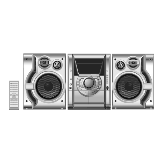
SA-AK331GCP
Colour
(S)... Silver Type
Mic jack
Terminal
n CASSETTE DECK SECTION
Track system
Heads
Record/playback
Erasure
Motor
Recording system
Erasing system
Tape speed
Overall frequency response (+3 dB, -6 dB at DECK OUT)
NORMAL
S/N
Wow and flutter
Fast forward and rewind time
n DISC SECTION
Discs played [8 cm or 12 cm]
(1) CD-Audio (CD-DA)
(2) CD-R/RW (CD-DA, MP3 formatted discs)
(3) MP3
Bit rate
MP3
Sampling frequency
MP3
© 2004 Matsushita Electric Industrial Co. Ltd.. All
rights
reserved.
distribution is a violation of law.
ORDER NO. MD0412582C3
CD Stereo System
0.7mV, 680 Ω
Mono, 3.5 mm
4 track, 2 channel
Solid permalloy head
Double gap ferrite head
DC servo motor
AC bias 100 kHz
AC erase 100 kHz
35 Hz - 14 kHz
50 dB (A weighted)
0.18 % (WRMS)
Approx. 120 seconds with
C-60 cassette tape
32 kbps - 320 kbps
32 kHz, 44.1 kHz, 48 kHz
Unauthorized
copying
4.8 cm/s
and
Advertisement
Table of Contents

Related Manuals for Panasonic SA-AK331GCP


Summary of Contents for Panasonic SA-AK331GCP
- Page 1 ORDER NO. MD0412582C3 CD Stereo System SA-AK331GCP Colour (S)... Silver Type Specifications n AMPLIFIER SECTION Mic jack 0.7mV, 680 Ω RMS output power Terminal THD 10%, both channels driven Mono, 3.5 mm 1 kHz, n CASSETTE DECK SECTION 90 W per channel (5 Ω)
-
Page 2: Table Of Contents
SA-AK33 1GCP 44.1 kHz Power consumption in standby 0.85 W mode Decoding 16 bit linear Dimensions (W x H x D) 250 x 330 x 341 mm Digital filter 8 fs Mass 7.1 kg D/A converter MASH (1 bit DAC) Operating temperature range +5 to +35°C Pickup... - Page 3 SA-AK33 1GCP 17.5. (D) Transformer Circuit, (E) CD Detect Circuit, (F) Spindle 21 Terminal Function of IC 痴 Position Circuit & (G) CD Loading Circuit 21.1. IC7002 (MN6627953HB) Servo processor/ Digital signal 17.6. (H) Power Circuit processor/ Digital filter/ D/A converter 17.7.
-
Page 4: Before Use
SA-AK33 1GCP 1 Before Use Be sure to disconnect the mains cord before adjusting the voltage selector. Use a minus(-) screwdriver to set the voltage selector (on the rear panel) to the voltage setting for the area in which the unit will be used. -
Page 5: Handling The Lead-Free Solder
SA-AK33 1GCP damage an ES device). 5 Handling the Lead-free Solder 5.1. About lead free solder (PbF) Distinction of PbF P.C.B.: P.C.B.s (manufactured) using lead free solder will have a PbF stamp on the P.C.B. Caution: · Pb free solder has a higher melting point than standard solder; Typically the melting point is 50 - 70°F (30 - 40°C) higher. Please use a high temperature soldering iron. -
Page 6: Handling Precautions For Traverse Deck
SA-AK33 1GCP 6 Handling Precautions For Traverse Deck The laser diode in the traverse deck (optical pickup) may break down due to potential difference caused by static electricity of clothes or human body. So, be careful of electrostatic breakdown during repair of the traverse deck (optical pickup). ·... -
Page 7: Precaution Of Laser Diode
SA-AK33 1GCP 7 Precaution of Laser Diode Caution : This product utilizes a laser diode with the unit turned "ON", invisible laser radiation is emitted from the pick up lens. Wavelength : 780 nm Maximum output radiation power from pick up : 100 µW/VDE Laser radiation from pick up unit is safety level, but be sure the followings: 1. -
Page 8: Accessories
SA-AK33 1GCP 8 Accessories Remote Control FM Antenna AC Cord AM Loop Antenna AC Plug Adaptor... -
Page 9: Operation Procedures
SA-AK33 1GCP 9 Operation Procedures... - Page 10 SA-AK33 1GCP...
-
Page 11: Disassembly And Assembly Of Main Component
SA-AK33 1GCP 10 Disassembly and Assembly of Main Component “ATTENTION SERVICER” Some chassis components may have sharp edges. Be careful when disassemblin g and servicing. 1. This section describes procedures for checking the operation of the major printed circuit boards and replacing the main components. -
Page 12: Gear For Servicing (Jig) Information
SA-AK33 1GCP 10.2. Gear for servicing (jig) Information 1. This unit has a gear which is used for checking items (Open/Close of disc tray, up/down operation of traverse unit by manually) when servicing. 2. For preparation of gear (for servicing), perform the procedures as follows. 3. -
Page 13: Disassembly Of Top Cabinet
SA-AK33 1GCP 10.3. Disassembly of Top Cabinet Step 1 Remove 2 screws at each side and 5 screws at rear panel. Step 2 Lift up both sides of the top cabinet, push the top cabinet towards the rear and remove the top cabinet. 10.4. - Page 14 SA-AK33 1GCP Step 6 Press the POWER button to turn the power off. · [Opening the disc tray manually (Using service tools)] Step 3 Repeat Step 2 but rotate the gear tools in anti-clockwise direction. Step 1 Insert the gear tool into the hole on the underside of CD chassis and then rotate in the direction of arrow.
-
Page 15: Disassembly Of Rear Panel
SA-AK33 1GCP 10.5. Disassembly of Rear Panel · Follow the (Step 1) - (Step 2) of Item 10.3 - Disassembly of Top Cabinet Step 1 Remove 8 screws and disconnect wire CN2810 (Fan) at rear cabinet as shown. 10.6. Disassembly of CD Mechanism Unit ·... -
Page 16: Disassembly Of Main P.c.b
SA-AK33 1GCP 10.7. Disassembly of Main P.C.B. · Follow the (Step 1) - (Step 2) of Item 10.3 - Disassembly of Top Cabinet · Follow the (Step 1) - (Step 6) of Item 10.4 - Disassembly of CD Lid · Follow the (Step 1) of Item 10.5 - Disassembly of Rear Panel ·... -
Page 17: Disassembly Of Transformer P.c.b
SA-AK33 1GCP · Replacement of the Power Amplifier IC/ Voltage Regulator Step 1 Remove 2 screws fixed to the Power Amplifier IC and 1 Step 3 Unsolder the terminals of Power Amp IC, transistor and screw to Voltage Regulator. replace the components. Step 4 Fix back the cut portion with a screw as shown. -
Page 18: Disassembly Of Front Panel Unit
SA-AK33 1GCP 10.10. Disassembly of Front Panel Unit · Follow the (Step 1) - (Step 2) of Item 10.3 - Disassembly of Top Cabinet · Follow the (Step 1) - (Step 6) of Item 10.4 - Disassembly of CD Lid ·... -
Page 19: Cd Mechanism Main Component Replacement Procedures
SA-AK33 1GCP Step 7 Unsolder the motor terminals. Step 8 Remove Deck Mechanism P.C.B. 10.12. CD Mechanism Main Component Replacement Procedures · Follow the (Step 1) - (Step 2) of Item 10.3 - Disassembly of Top Cabinet · Follow the (Step 1) - (Step 6) of Item 10.4 - Disassembly of CD Lid ·... - Page 20 SA-AK33 1GCP Step 6 Lift up the traverse deck ass’y. Step 10 Remove the FFC board from the connector, and then remove the CD Servo P.C.B. Step 7 Remove the traverse deck ass’y from the timing lever. Caution: When removing or inserting the traverse deck avoid touching the OPU lens and pressing onto the turntable.
- Page 21 SA-AK33 1GCP Note: Step 1 Install the traverse deck ass’y to the timing lever. Be careful not to lose the 3 floating spring because those will Step 2 Align the boss of traverse deck ass’y with the slot of also be removed on removal of the traverse deck ass’y. traverse cam gear.
- Page 22 SA-AK33 1GCP Step 5 With pressing the claw (B) in the direction of arrow (1), force the connection lever in the direction of arrow (2). 10.12.2. Replacement for the Disc Tray Step 1 Remove 4 screws. Step 2 Remove the upper plate. Step 3 Remove 3 screws.
- Page 23 SA-AK33 1GCP Step 6 Insert the gear with hexagonal wrench into the hole. Step 9 With forcing the left guide bar manually because the left guide bar interfers with claw, draw the disc tray. [Installation of the disc tray after replacement] Step 7 Rotate the hexagonal wrench in the direction of arrow, and then open the disc tray fully.
- Page 24 SA-AK33 1GCP NOTE: Force the right guide bar of tray base manually not to move upwards. Step 4 Holding the disc tray manually, push the disc tray in the direction of the arrow. 10.12.3. Disassembly and reassembly for mechanism base drive unit Step 1 Remove 3 screws.
- Page 25 SA-AK33 1GCP Step 9 Pressing the claw (B) in the direction of arrow (1), force the connection lever in the direction of arrow (2). Step 6 Install the tray lock spring to hook temporary. Step 7 Release the claw, and then remove the tray lock. Step 8 Release the claw, and then remove the rear lock.
- Page 26 SA-AK33 1GCP Step 13 Remove the traverse relay gear, traverse cam gear and drive gear. Step 11 Lift up the left end of spindle base unit in the direction of arrow (1), and then remove the unit in the direction of arrow (2).
- Page 27 SA-AK33 1GCP Step 3 Rotate the disc lever in the direction of arrow (1), draw the disc lever. NOTE: Hold the loading stopper ass’y manually bacause it is flipped by spring. NOTE: Take care not to lose the disc lever spring. Step 6 Remove the cushion spring.
- Page 28 SA-AK33 1GCP Step 8 Release the 2 claws, and then remove the relay gear A. Step 9 Release the 2 claws, and then remove the spindle shaft. Step 12 Squeeze the shaft of lower hook, and then draw it. Step 13 Rotate the lower spindle in the direction of arrow until Step 10 Remove the lower spindle spring with tweezers.
- Page 29 SA-AK33 1GCP spread the hold bars of loading stopper and remove the Step 1 Install the traverse cam gear. UP/DOWN base. Step 2 Rotate the traverse cam gear to the direction of arrow. [Installation for loading stopper ass’y] Step 1 Align the claw of loading stoppers ass’y with the slot of spindle base.
- Page 30 SA-AK33 1GCP Step 4 Install the slide plate 2 to the mechanism base, and then match to the connection lever. Step 7 Move the slide plate 1 to forward fully. Step 5 Install the slide plate 1 to the mechanism base, and then match to the connection leve and align the trapezoid tooth Step 8 Install the rear lock.
- Page 31 SA-AK33 1GCP Step 13 Install the gear holder, and then tighten the screw (a). Step 11 Remove the tray lock spring from hook,and then latch to the tray lock. Step 12 Install the UP/DOWN gear, change gear, change gear spring, pulley gear and belt in the order of (1) - (5). Step 14 Install the tray base, traverse ass’y, mechanism cover and upper plate.
-
Page 32: Replacement For The Pinch Roller Ass 馳 And Head Block
SA-AK33 1GCP 10.12.4. Replacement for the motor ass’y Step 1 Install the belt temporarily. NOTE: Take care not apply the grease to the belt. Step 6 Release the 2 claws (A), and then remove the Motor Step 2 Upset the CD loading unit. P.C.B. -
Page 33: Replacement For The Deck Motor Ass 馳, Capstan Belt A, Capstan Belt B And Winding Belt
SA-AK33 1GCP Step 1 Release the 2 claws, and then remove the pinch roller (R), (F). Step 2 Release the 2 claws, and then remove the head connector. Step 3 Remove 2 screws. 10.14. Replacement for the Deck motor ass’y, capstan belt A, capstan belt B and winding belt ·... - Page 34 SA-AK33 1GCP Step 5 Remove the flywheel R. Step 6 Release the claw of tape side, and then remove the winding lever and spring. Step 7 Remove the flywheel F. [Installation of the belt] Step 1 The boss and marking should be positioned Step 2 Put the winding belt on the pulley temporarily.
- Page 35 SA-AK33 1GCP Step 7 Put the capstan belt A temporarily as shown below. Step 10 Remove 3 screws. Step 11 Put the capstan belt B as shown below. Step 8 Put the capstan belt B on the motor ass’y pulley. Step 12 Put the capstan belt A on the motor ass’y pulley.
-
Page 36: Replacement For The Cassette Lid Ass 馳
SA-AK33 1GCP 10.15. Replacement for the cassette lid ass’y · Follow the (Step 1) - (Step 2) of Item 10.3 - Disassembly of Top Cabinet Step 1 Lift up the lever upward, open the cassette lid ass’y. (For DECK1 and DECK2) Step 2 Push up the cassette lid ass’y in the direction of arrow. -
Page 37: Rectification For Tape Jam Problem
SA-AK33 1GCP 10.16. Rectification for tape jam problem · Follow the (Step 1) - (Step 2) of Item 10.3 - Disassembly of Top Cabinet Step 1 If a cassette tape cannot be removed from the deck (the tape is caught by the capstan or pinch roller during playback or recording), rotate the flywheel F in the direction of the arrow to remove it. -
Page 38: Checking For Major P.c.bs
SA-AK33 1GCP 11 Checking for major P.C.Bs Note: Checking of all major P.C.Bs (Main P.C.B., Panel P.C.B., Transformer P.C.B., Deck P.C.B., Deck Mechanism P.C.B. and Power P.C.B.) can be carried out using below procedures. For the disassemblin g procedures, refer to Section 10. 11.1. -
Page 39: Checking Of Transformer P.c.b
SA-AK33 1GCP 11.2. Checking of Transformer P.C.B. 1. Remove Top Cabinet and Rear Panel. 2. Remove CD Lid. 3. Disassemble CD Mechanism Unit. 4. Connect FFC wires (CN2801 & CN2805) from CD Mechanism Unit. -
Page 40: Checking Of Panel, Deck & Deck Mechanism P.c.b
SA-AK33 1GCP 11.3. Checking of Panel, Deck & Deck Mechanism P.C.B. 1. Remove Top Cabinet. 2. Remove CD Lid. 3. Disassemble CD Mechanism Unit. 4. Remove volume knob at Front Panel Unit. 5. Disassemble Panel P.C.B. 6. Disassemble Deck Mechanism Unit. 7. -
Page 41: Checking Of Power P.c.b
SA-AK33 1GCP 11.4. Checking of Power P.C.B. 1. Remove Top Cabinet and Rear Panel. 2. Remove CD Lid. 3. Disassemble CD Mechanism Unit. 4. Remove 3 screws at Transformer P.C.B.. 5. Remove 2 screws at heat sink and 1 screw at Power P.C.B. 6. -
Page 42: Self-Diagnostic Function
SA-AK33 1GCP 12 Self-Diagnostic Function 12.1. Self-diagnostic display This unit is equipped with a self-diagnost ic display function which, will display an error code corresponding to the problem occuring. Use this function when performing checking maintenance on the unit. 12.2. How to enter the Self-Diagnostic Function 12.3. -
Page 43: To Clear All Error Code
SA-AK33 1GCP 7. Press “n/STOP” to indicate Error Code. · If several problem exist, error code will change each time when “n/STOP” is pressed. (e.g. F15 → F26 → F16 ..etc). 12.5. To clear all Error code 1. Press and hold button for 5 seconds. 2. - Page 44 SA-AK33 1GCP 2. Reset Condition of Error Code a. During cold start of micro-processor IC. b. Restart of aging mode for the mechanism unit. 3. Mechanism Error Code Mechansim Error Code Table Error Code Description M-00 No Error M-01 OPEN Position - Horizontal Motion Abnormality at play position M-02 PLAY Position - Horizontal Motion Abnormality at stock position M-03...
-
Page 45: Cd Test Mode Function
SA-AK33 1GCP 13 CD Test Mode Function This CD test mode is provided to check CD unit without connecting to changer loading mechanism. This mode shall operate CD PLAY with CD unit being connected only and CD Automatic Alignment result is shown on FL display. 13.1. -
Page 46: Micon Rom Checksum And Version Display Mode
SA-AK33 1GCP 13.4. Micon ROM Checksum and Version Display Mode 1. Functional Summary Display version number and calculated checksum of the micon software. 2. To enter into Micon ROM checksum and Version Display Mode. a. Enter into Self-Diagnos tic Mode (Refer to Section 12.2). b. -
Page 47: Measurements And Adjustments
SA-AK33 1GCP 14 Measurements and Adjustments 14.1. Cassette Deck Section standard value. Bias voltage for Deck 2 14±4mV (Normal) · Measurement Condition Erase voltage for Deck 2 80mV (Normal) − − − − Make sure head, capstan and press roller are clean. −... -
Page 48: Alignment Points
SA-AK33 1GCP 9. Set AM-SG to 520kHz. 10. Receive 520kHz in the unit. 11. Adjust L2602 (OSC) so that the EVM-DC value is with 1.1±0.5V. Fig.6 14.2.2. AM RF Adjustment 1. Connect the instrument as shown in Fig. 7. 2. Set the unit to AM mode. 3. -
Page 49: Block Diagram
SA-AK33 1GCP 15 Block Diagram OPTICAL PICKUP SEMICONDUCTOR LASER Q7601 LASER POWER DRIVE PHOTO DETECTOR IC7003 AN8739SBTE2 FOCUS COIL/TRACKING COIL/ TRAVERSE MOTOR/ SPINDLE MOTOR DRIVE /RST RESET SIGNAL GENERATOR FOCUS FOCUS COIL COIL DRIVE TRACKING COIL TRACKING COIL DRIVE TRAVERSE M7301 TRVP MOTOR... - Page 50 SA-AK33 1GCP TO MAIN BLOCK X7201 NTEST IOMODE CD_RST NRST TXTCK MICRO COMPUTER TIMING GENERATOR DSL/PLL/VCO INTERFACE TXTD DQSY RFVDD (SBCK) EFM DEMODULATION SUBCODE (SUBC) SPINDLE VREF SYNC INTERPOLATION INTERFACE SERVO CIRC ECC (TXNCLDCK) CDROM ECC A, B, C, D, E, F 30~35 A,B,C,D,E,F FLAG...
- Page 51 SA-AK33 1GCP AM ANT FM ANT Z2620 CF2601 CF2602 Q1 (RF AMP) Q2601 MIXER IF AMP D2602 L2602 L2601 BUFFER (FM) DECODER RM AMP BUFFER PHASE PILOT CANCEL STEREO LEVEL S-CURVE SWITCH AM/FM COMP BUFFER TUNING DRIVE PILOT IC2601 X2602 LA1833NMNTLM Z2602 FM/AM IF AMP,...
- Page 52 SA-AK33 1GCP FL6602 FROM POWER FL DISPLAY TRANSFORMER 23~40 5~19 1,2, 11~14, 16~29 30~40 IC6601 C0HBB0000044 FL DRIVER C0GAM0000005 MOTOR DRIVE OUT1 OUT2 POWER SUPPLY CONTROL PLLDA Q2907 STAT SWITCH PUSH Q2936 PUSH MOTOR ST/DO SUPPLY SWITCH OPEN PLLCLK Q2906 BLKCK Q2937 SWITCH...
- Page 53 SA-AK33 1GCP IC1001 AN7348S-E1 P.B EQ/REC AMP/ ALC/TPS AMP 24(23) (DECK 1) P.B. HEAD 1(2) 20(5) 22(3) 21(4) 17(8) (DECK 2) R/P HEAD 18(7) LOGIC L/H NOR/CrO & HI/LO LOGIC RIPPLE LOGIC REJECTION REC/PB Q6501, Q6502 JK6501 Q2978 SWITCH (DECK 2) ERASE HEAD L1002 BIAS OSC...
- Page 54 SA-AK33 1GCP IC2804 7(8) B1(2) C0AABA000009 DUAL OP-AMP Q2181 (Q2281) 13(14) JK2801 E1(2) 22(21) 2(6) OUT1(2) HPF FREQ 1(7) FILTER 3(5) SWITCH 9(10) Q2142 (Q2242) CD SIGNAL C1(2) CONTROL 5(6) IC2806 A1(2) C0ABBB000244 DUAL OP-AMP FILTER IC2803 C1BB00000732 AUDIO SOUND 32(31) PROCESSOR REC1(2)
- Page 55 SA-AK33 1GCP 16(15) 3(6) -IN2 1(2) OUT 2 1(2) HIGH CH (6 W) IC5801 JK5951 (JK5952) RSN315H42C-P POWER HIC 7(9) 13(12) OUT 1 1(2) -IN1 1(2) LOW CH (6 W) 4(2) +VCC 1(2) 5(1) -VCC 1(2) IN GND D5814 OUT GND AC DET -VCCM FILTER...
-
Page 56: Voltage Measurement
SA-AK33 1GCP 16 Voltage Measurement... - Page 57 SA-AK33 1GCP...
-
Page 58: Schematic Diagram
SA-AK33 1GCP 17 Schematic Diagram · Do not touch the pins of IC, LSI or VLSI with fingers directly. (All schematic diagrams may be modified at any time with the development of the new technology) Note: : Push switch : Push switch : Open switch : CD switch : Load switch... -
Page 59: A) Cd Servo Circuit
SA-AK33 1GCP 17.1. (A) CD Servo Circuit SCHEMATIC DIAGRAM - 1 : +B SIGNAL LINE : CD-DA SIGNAL LINE OPTICAL PICKUP CIRCUIT CD SERVO CIRCUIT Q7601 LASER DIODE B1ADCF000001 R7601 C7601 C7670 C7204 C7203 LASER POWER DRIVE 6.3V33 6.3V220 Q7601 R7650 LD GND NBOUT... - Page 60 SA-AK33 1GCP SCHEMATIC DIAGRAM - 2 : +B SIGNAL LINE : CD-DA SIGNAL LINE : CD SIGNAL LINE CD SERVO CIRCUIT C7626 C7625 C7224 C7223 6.3V220 6.3V100 R7217 C7225 1000P C7226 R7211 1000P R7218 R7221 C7231 C7230 6.3V220 R7212 C7234 C7233 C7232 16V10...
-
Page 61: B) Main (Tuner) Circuit
SA-AK33 1GCP 17.2. (B) Main (Tuner) Circuit SCHEMATIC DIAGRAM - 3 : +B SIGNAL LINE : FM SIGNAL LINE : AM SIGNAL LINE : FM/AM SIGNAL LINE : FM OSC SIGNAL LINE : AM OSC SIGNAL LINE MAIN (TUNER) CIRCUIT R2604 Q2606 TUNER PACK CIRCUIT... -
Page 62: B) Main Circuit
SA-AK33 1GCP 17.3. (B) Main Circuit SCHEMATIC DIAGRAM - 4 : PLAYBACK SIGNAL LINE : AUX SIGNAL LINE : +B SIGNAL LINE : -B SIGNAL LINE : RECORD SIGNAL LINE : MAIN SIGNAL LINE MAIN CIRCUIT Q2980 Q2978 B1GDCFJJ0023 B1GDCFJJ0023 DECK MOTOR SWITCH CR02 SWITCH... - Page 63 SA-AK33 1GCP SCHEMATIC DIAGRAM - 5 : CD SIGNAL LINE : +B SIGNAL LINE PANEL CIRCUIT : -B SIGNAL LINE (CN6601) ON : MAIN SIGNAL LINE SCHEMATIC DIAGRAM-10 MAIN CIRCUIT CN2806 36 35 34 33 32 31 30 29 28 27 26 25 15 14 13 12 11 10 R2006 C2752...
- Page 64 SA-AK33 1GCP SCHEMATIC DIAGRAM - 6 : -B SIGNAL LINE : +B SIGNAL LINE TO FAN UNIT MAIN CIRCUIT CN2810 R2595 R2414 R2420 R2591 R2338 D2332 330K B0ADCC000002 C2415 R2415 R2413 R2337 C2334 R2333 C2332 470K 0.22 R2331 R2419 R2412 5.6K R2715 C2414...
- Page 65 SA-AK33 1GCP SCHEMATIC DIAGRAM - 7 : +B SIGNAL LINE MAIN CIRCUIT VREF+ 64 63 R2827 R2830 R2831 MCLK MCLK RESTSW /RESTSW CHG_HLF CHG_HLF DCDET CHG_CW R2834 CHG_CW DCDET CHG_CCW PCONT CHG_CCW PCONT/EFP_/CE CHG_SW1 CHG_SW1 CHG_SW2 CHG_SW2 CHG_PLR EE_DAT CHG_PLR EE_DAT EE_CLK CHG_AD2...
- Page 66 SA-AK33 1GCP SCHEMATIC DIAGRAM - 8 : +B SIGNAL LINE : AUX SIGNAL LINE : MAIN SIGNAL LINE : -B SIGNAL LINE : CD SIGNAL LINE : PLAYBACK SIGNAL LINE : RECORD SIGNAL LINE : FM/AM SIGNAL LINE MAIN CIRCUIT D2951 B0BC7R500001 C2952...
-
Page 67: C) Panel Circuit
SA-AK33 1GCP 17.4. (C) Panel Circuit SCHEMATIC DIAGRAM - 9 : MAIN SIGNAL LINE : +B SIGNAL LINE : -B SIGNAL LINE PANEL CIRCUIT SYS6V S6210 R6458 DECK1 4.7K OPEN D6458 S6209 B3AAA00000583 POWER KEY3 S6301 R6399 S6208 OPEN/CLOSE TAPE VREF+ VR6491 R6199... - Page 68 SA-AK33 1GCP SCHEMATIC DIAGRAM - 10 : +B SIGNAL LINE : -B SIGNAL LINE : MAIN SIGNAL LINE PANEL CIRCUIT MICSW R6506 C6505 R6503 2.2K 0.047 R6501 R6509 C6509 C6506 C6501 0.01 C6503 50V1 0.01 C6510 C6504 0.047 50V1 50V0.1 R6505 330K C6502...
-
Page 69: D) Transformer Circuit, (E) Cd Detect Circuit, (F) Spindle Position Circuit & (G) Cd Loading Circuit
SA-AK33 1GCP 17.5. (D) Transformer Circuit, (E) CD Detect Circuit, (F) Spindle Position Circuit & (G) CD Loading Circuit SCHEMATIC DIAGRAM - 11 : +B SIGNAL LINE : -B SIGNAL LINE TRANSFORMER CIRCUIT D5950-D5953 S5950 B0EAMM000038 VCC+ D5950 D5952 VCC- 250V 1.6A A: 240V C5960... -
Page 70: H) Power Circuit
SA-AK33 1GCP 17.6. (H) Power Circuit SCHEMATIC DIAGRAM - 12 : -B SIGNAL LINE : MAIN SIGNAL LINE : +B SIGNAL LINE POWER CIRCUIT IC5801 IC5801 RSN315H42C-P POWER HIC C5801 HIGH 0.01 C5445 CHANNEL C5245 R5857 R5855 R5452 R5252 SPEAKER 0.047 0.047 D5814... -
Page 71: I) Deck Circuit & (J) Deck Mechanism Circuit
SA-AK33 1GCP 17.7. (I) Deck Circuit & (J) Deck Mechanism Circuit SCHEMATIC DIAGRAM -13 : +B SIGNAL LINE : PLAYBACK SIGNAL LINE : RECORD SIGNAL LINE DECK CIRCUIT C1038 R1055 C1057 220P C1034 2.2K 1000P 50V3.3 C1044 R1101 R1100 R1015 10V33 C1032 0.018... - Page 72 SA-AK33 1GCP SCHEMATIC DIAGRAM - 14 : PLAYBACK SIGNAL LINE : +B SIGNAL LINE : RECORD SIGNAL LINE MAIN CIRCUIT (CN2803) ON SCHEMATIC DIAGRAM-4 DECK CIRCUIT CN1001 14 13 12 11 10 R1098 R1060 R1057 2.2K R1091 R1097 R1092 W1002 R1049 R1084 Q1017...
-
Page 73: Printed Circuit Board
SA-AK33 1GCP 18 Printed Circuit Board Note: Circuit board diagrams may be modified at any time with the development of new technology. 18.1. (A) CD Servo P.C.B. CD SERVO P.C.B (REPX0443A) C7670 R7217 C7223 C7601 C7106 C7105 W7011 R7212 TP22 TP29 C7204 W7040... -
Page 74: B) Main
SA-AK33 1GCP 18.2. (B) Main P.C.B. MAIN P.C.B (REPX0442G) CN2810 W2257 TO FAN W2236 R2940 W2258 CN2805 Q2706 W2259 R2709 D2705 Q2704 W2260 R2715 Q2705 W2261 Q2936 W2248 D2704 W2265 W2249 D2936 D2703 W2262 R2702 R2858 R2860 Q2701 W2250 Q2937 W2263 Q2702 R2859... - Page 75 SA-AK33 1GCP W2257 Q2901 R2902 W2258 C2902 W2259 R2910 Q2902 W2515 W2260 W2261 D2901 W2265 CN2801 W2262 R2860 W2263 R2859 W2266 R2903 W2268 R2917 C2814 D2904 W2267 R2918 W2208 W2269 W2905 Q2906 W2275 W2504 W2508 2255 W2276 2256 W2270 W2904 Q2907 W2277 R2929...
-
Page 76: C) Panel
SA-AK33 1GCP 18.3. (C) Panel P.C.B. PANEL P.C.B (REPX0441B) W6991 W6994 W6992 W6993 FL6602 C6631 W6996 W6100 C6623 C6481 W6005 Z6481 S6101 J6481 W6006 C6612 W6002 R6611 OPEN/ CLOSE C6635 R6102 S6102 R6111 W6045 W6044 W6046 S6103 W6079 J6108 S6104 W6032 S6204 W6030... - Page 77 SA-AK33 1GCP CN6601 FL6602 R6458 W6105 J6902 W6100 D6458 W6089 W6075 C6636 W6063 W6083 W6076 S6301 W6062 IC6601 W6082 W6085 W6102 W6065 R6611 W6033 POWER W6103 W6094 W6080 W6059 C6632 W6081 W6066 R6199 W6077 W6071 J6108 W6034 R6302 W6010 S6303 D6457 W6049 SSEQ...
-
Page 78: D) Transformer
SA-AK33 1GCP 18.4. (D) Transformer P.C.B. TRANSFORMER P.C.B (REPX0467D) CAUTION RISK OF ELECTRIC SHOCK AC VOLTAGE LINE. PLEASE DO NOT TOUCH THIS P.C.B 125V 3.15A T5951 C5962 SUB-TRANSFORMER R5957 Q5952 250V 1.6A C5963 W5938 RL5950 Q5953 W5919 JK5950 R5951 W5920 C5964 W5989 Q5954... - Page 79 SA-AK33 1GCP 18.5. (E) CD Detect P.C.B., (F) Spindle Position P.C.B., (G) CD Loading P.C.B. & (K) Tuner Pack P.C.B. CD LOADING P.C.B (REP2578A-N) OPEN PUSH PUSH CD DETECT P.C.B SPINDLE POSITION P.C.B (REP2578A-N) (REP2578A-N) LOAD TUNER PACK P.C.B (REP1999B)
-
Page 80: H) Power
SA-AK33 1GCP 18.6. (H) Power P.C.B. POWER P.C.B (REPX0469G) H5950/W5950 Q5801 Q5803 Q5804 Q5802 W5809 R5814 R5823 R5813 D5801 R5828 C5809 C5804 C5806 C5811 R5825 R5835 W5834 C5805 R5826 W5836 W5846 W5824 R5802 Q5806 R5818 W5864 R5827 W5804 Q5814 R5834 R5812 J5803 R5819... - Page 81 SA-AK33 1GCP IC5801 JK5951 W5870 W5808 1 +L W5869 J5453 W5551 W5881 R5450 J5253 2 +R D5802 W5552 HIGH W5825 W5824 R5802 CHANNEL Q5814 3 -L C5445 R5456 4 -R C5245 R5805 R5448 W5550 Q5813 Q5812 1 -L R5256 2 -R R5255 W5847 CHANNEL...
-
Page 82: I) Deck P.c.b. & (J) Deck Mechanism
SA-AK33 1GCP 18.7. (I) Deck P.C.B. & (J) Deck Mechanism P.C.B. DECK P.C.B. DECK MECHANISM P.C.B. (REPX0331D) (REPX0321B) R1024 IC1004 C1006 C1009 R1027 CS1002 TP10 Q1003 J1002 L1002 TP11 R1004 R1001 Q1007 W1002 C1002 C1026 J1003 TP12 S951 C1021 C1020 C1011 Q1017 MODE... -
Page 83: Wiring Connection Diagram
SA-AK33 1GCP 19 Wiring Connection Diagram FM ANT AM ANT H5950/ W5950 JK2601 JK2801 To Fan CD LOADING P.C.B CN5801 CN2809 CN2810 TUNER PACK SOLDER SIDE P.C.B MAIN P.C.B SOLDER SIDE CN2805 TUNER PACK CD DETECT P.C.B SOLDER SIDE 13 14 BLACK POWER P.C.B SOLDER SIDE... -
Page 84: Illustration Of Ic 痴, Transistors And Diodes
SA-AK33 1GCP 20 Illustration of IC’s, Transistors and Diodes RSN315H42C-P C2CBJG000564 (100P) C0AABA000009 C1AA00000612 C0HBB0000044 (48P) AN7348S-E1 (24P) MN6627953HB (80P) LA1833NMNTLM (24P) LC72131MDTRM (20P) C1BB00000732 (32P) AN8739SBTE2 CNB13030R2AU C0GAM0000005 C0ABBB000244 2SB0709AHL 2SD0601AHL B1ADCF000001 B1ABCF000131 B1GDCFJJ0023 B1GBCJFF0039 B1AAGC000007 B1BACG000023 B1AAAC000011 B1GACFGG0004 B1ACKD000004 B1BCCG000002 B1AAAD000013... -
Page 85: Ic7002 (Mn6627953Hb) Servo Processor/ Digital Signal
SA-AK33 1GCP 21 Terminal Function of IC’s 21.1. IC7002 (MN6627953HB) Servo Pin No. Mark Function AVDD2 Analog circuit power supply 2 processor/ Digital signal OUTL LCH output signal processor/ Digital filter/ D/A AVSS1 Audio output circuit GND 1 N.C. No Connection converter AVDD1 Power supply 1 for analog... -
Page 86: Ic2801 (C2Cbjg000564) System Microprocessor
SA-AK33 1GCP Pin No. Mark Function Pin No. Mark Function Motor driver (2) forward- action MUTE_A Audio Mute output EE_CS/EFP_/EPM O EEPROM Chip Select Motor driver (3) reverse- action EE_CLK EEPROM Clock output EE_DAT I/O EEPROM Data Crystal oscillating circuit input (f = N.C. -
Page 87: Troubleshooting Guide
SA-AK33 1GCP 22 Troubleshooting Guide... -
Page 88: Parts Location And Replacement Parts List
SA-AK33 1GCP 23 Parts Location and Replacement Parts List Notes: · Important safety notice: Components identified by mark have special characteristic s important for safety. Furthermore, special parts which have purposes of fire-retardent (resistors), high-quality sound (capacitors), low noise (resistors), etc are used. When replacing any of these components, be sure to use only manufacturer’s specified parts shown in the parts list. -
Page 89: Deck Mechanism (Raa3412-S)
SA-AK33 1GCP 23.1. Deck Mechanism (RAA3412-S) 23.1.1. Deck Mechanism Parts Location... - Page 90 SA-AK33 1GCP...
- Page 91 SA-AK33 1GCP 23.1.2. Deck Mechanism Parts List Ref. No. Part No. Part Name & Description Remarks CASSETTE DECK RED0071 R/P HEAD BLOCK UNIT RED0072 P/B HEAD BLOCK UNIT RDG0300 REEL BASE GEAR RDG0301 WINDING RELAY GEAR RDK0026 MAIN GEAR RDR0029-3 RELAY PULLEY RDV0033-4 WINDING BELT...
-
Page 92: Cd Loading Mechanism (Rd-Dac026-S)
SA-AK33 1GCP 23.2. CD Loading Mechanism (RD-DAC026-S) 23.2.1. CD Loading Mechanism Parts Location... - Page 93 SA-AK33 1GCP...
- Page 94 SA-AK33 1GCP 23.2.2. CD Loading Mechanism Parts List Ref. No. Part No. Part Name & Description Remarks Ref. No. Part No. Part Name & Description Remarks TRAVERSE DECK XTN2+6G SCREW RMX0141 PUSH SPACER RML0517 TIMING LEVER RMQ0749 UPPER SPINDLE RML0516 PLUNGER LEVER RHM0001 MAGNET...
-
Page 95: Cabinet
SA-AK33 1GCP 23.3. Cabinet 23.3.1. Cabinet Parts Location... - Page 96 SA-AK33 1GCP...
-
Page 97: Electrical Parts List
SA-AK33 1GCP 23.3.2. Cabinet Parts List Ref. No. Part No. Part Name & Description Remarks Ref. No. Part No. Part Name & Description Remarks CABINET AND CHASSIS RKMX0105- S TOP CABINET RMBX0036 CASS OPEN SPRING L6FALEFH0030 RMCX0021 TRANSISTOR CLIP REEX0202 10P FFC (PANEL) RMKX0099 BOTTOM CHASSIS... - Page 98 SA-AK33 1GCP Ref. No. Part No. Part Name & Description Remarks Ref. No. Part No. Part Name & Description Remarks Q6502 B1AACF000064 TRANSISTOR S971 K0J1BB000017 SW MODE Q7601 B1ADCF000001 TRANSISTOR S972 RSH1A019- 2U SW HALF S974 RSH1A019- 2U SW RECINH_R DIODES S975 RSH1A019- 2U...
- Page 99 SA-AK33 1GCP Ref. No. Part No. Part Name & Description Remarks Ref. No. Part No. Part Name & Description Remarks T5951 RTP1H3E002 BACK UP TRANSFORMER W2903 ERJ3GEY0R00V CHIP JUMPER W2904 ERJ3GEY0R00V CHIP JUMPER COMPONENT COMBINATIONS W2905 ERJ3GEY0R00V CHIP JUMPER W2906 ERJ3GEY0R00V CHIP JUMPER Z971...
- Page 100 SA-AK33 1GCP Ref. No. Part No. Part Name & Description Remarks Ref. No. Part No. Part Name & Description Remarks ERDS2TJ104T 100K 1/4W R2142 ERJ3GEYJ223V 22K 1/16W ERDS2TJ564T 560K 1/4W R2143 ERJ3GEYJ104V 100K 1/16W ERDS2TJ391T 390 1/4W R2145 ERJ3GEYJ103V 10K 1/16W ERDS2TJ272T 2.7K 1/4W R2146...
- Page 101 SA-AK33 1GCP Ref. No. Part No. Part Name & Description Remarks Ref. No. Part No. Part Name & Description Remarks R2403 ERJ3GEYJ334V 330K 1/16W R2628 ERJ3GEYJ820V 82 1/16W R2404 ERJ3GEYJ823V 82K 1/16W R2629 ERJ3GEYJ273V 27K 1/16W R2412 ERJ3GEYJ683V 68K 1/16W R2630 ERJ3GEYJ103V 10K 1/16W...
- Page 102 SA-AK33 1GCP Ref. No. Part No. Part Name & Description Remarks Ref. No. Part No. Part Name & Description Remarks R2886 ERJ3GEYJ105V 1M 1/16W R5806 ERDS2TJ104T 100K 1/4W R2891 ERJ3GEYJ473V 47K 1/16W R5807 ERDS1FVJ271T 270 1/2W R2892 ERJ3GEY0R00V 0 1/16W R5808 ERDS1FVJ271T 270 1/2W...
- Page 103 SA-AK33 1GCP Ref. No. Part No. Part Name & Description Remarks Ref. No. Part No. Part Name & Description Remarks R6405 ERDS2TJ274T 270K 1/4W F1D1H102A029 1000P 50V R6406 ERDS2TJ274T 270K 1/4W C1002 ECEA1HKN2R2B 2.2 50V R6411 ERDS2TJ223T 22K 1/4W C1006 ECEA1HKA010B 1 50V R6412...
- Page 104 SA-AK33 1GCP Ref. No. Part No. Part Name & Description Remarks Ref. No. Part No. Part Name & Description Remarks C2194 ECEA1CKA100B 10 16V C2606 ECJ1VB1H103K 0.01 50V C2201 ECJ1VB1C105K 1 16V C2607 ECJ1VB1E473K 0.047 25V C2202 ECJ1VB1C104K 0.1 16V C2608 ECJ1VC1H080D 8P 50V...
-
Page 105: Packing Materials & Accessories Parts List
SA-AK33 1GCP Ref. No. Part No. Part Name & Description Remarks Ref. No. Part No. Part Name & Description Remarks C2906 ECJ1VB1H102K 1000P 50V C6508 ECEA1AKA101B 100 10V C2907 ECJ1VB1H471K 470P 50V C6509 ECEA1HKA010B 1 50V C2936 ECJ1VF1C474Z 0.47 16V C6510 ECEA1HKA010B 1 50V... -
Page 106: Packaging
SA-AK33 1GCP Ref. No. Part No. Part Name & Description Remarks K2DA42E00001 AC PLUG ADAPTOR 23.6. Packaging PRT0412 P/S/J/N/A/E...
Need help?
Do you have a question about the SA-AK331GCP and is the answer not in the manual?
Questions and answers