Table of Contents
Advertisement
Service Manual
TOP NEXT
ORDER NO. MD0011177C1
A6
CD Stereo System
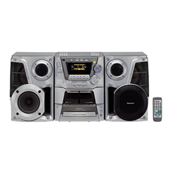
SA-AK33
l
Chassis
Colour
(S)... Silver Type
Area
(P)... U.S.A.
(PC)... Canada
TAPE SECTION :
SG2 MECHANISM SERIES
CD SECTION :
RAE0152Z-3 TRAVERSE DECK SERIES
Specifications
AMPLIFIER SECTION
Power output
THD 10% Total harmonic distortion
(HIGH)
(LOW)
(TOTAL)
Input sensitivity
AUX
Input Impedance
AUX
FM TUNER SECTION
Frequency range
Sensitivity
S/N 26 dB
Antenna terminal(s)
AM TUNER SECTION
Frequency range
Sensitivity
S/N 20 dB (at 1000 kHz)
CASSETTE DECK SECTION
Track system
Heads
Record/playback
Erasure
Motor
Recording system
Erasing system
Tape speed
Frequency response (+3 dB, -6 dB at DECK OUT)
NORMAL (TYPE I)
HIGH (TYPE II)
S/N
Wow and flutter
Fast forward and rewind time
http://servis-manual.com/
35-40 W per channel (6Ω)
85-90 W per channel (6Ω)
120-130 W per channel
250 mV
13 kΩ
87.9 - 107.9 MHz (200 kHz steps)
87.5 - 108.0 MHz (100 kHz steps)
2.5μV (IHF)
2.2μV
75Ω (unbalanced)
520 - 1710 kHz (10 kHz steps)
560μV/m
4 track, 2 channel
Solid permalloy head
Double gap ferrite head
DC servo motor
AC bias 100 kHz
AC erase 100 kHz
4.8 cm/s
35 Hz - 14 kHz
35 Hz - 14 kHz
50 dB (A weighted)
0.18% (WRMS)
Approx. 120 seconds with
Advertisement
Table of Contents

Related Manuals for Panasonic SA-AK33


Summary of Contents for Panasonic SA-AK33
- Page 1 Service Manual TOP NEXT ORDER NO. MD0011177C1 CD Stereo System SA-AK33 Chassis Colour (S)... Silver Type Area (P)... U.S.A. (PC)... Canada TAPE SECTION : SG2 MECHANISM SERIES CD SECTION : RAE0152Z-3 TRAVERSE DECK SERIES Specifications AMPLIFIER SECTION Power output THD 10% Total harmonic distortion (HIGH) 35-40 W per channel (6Ω)
-
Page 2: Self-Diagnostic Display
9.1 Self-diagnostic display TOP PREVIOUS NEXT This unit is equipped with a self-diagnostic display function which, if a problem occurs, will display an error code corresponding to the problem. Use this function when performing maintenance on the unit. TOP PREVIOUS NEXT http://servis-manual.com/... -
Page 3: How To Enter The Self-Diagnostic Function
9.2 How to enter the Self-Diagnostic Function TOP PREVIOUS NEXT TOP PREVIOUS NEXT... -
Page 4: Cassette Mechanism Test
9.3 Cassette Mechanism Test (For error code H01, H02, H03, F01, F02) TOP PREVIOUS NEXT 1. Press “TAPE, DECK 1/2” to select Deck 2. 2. Load a cassette tape with the erasure prevention tab, remove from left side only and close the cassette holder. -
Page 5: Cd Mechanism Test
9.4 CD Mechanism Test (F15, F26, F16, F17, F27, F28, F29, H15) TOP PREVIOUS NEXT 1. Press “CD”. 2. Press “OPEN/CLOSE (1)” and place a CD. 3. Press “OPEN/CLOSE (1)” to close the tray. 4. Press “OPEN/CLOSE (5)” and wait until the tray is open. 5. -
Page 6: To Clear All Error Code
9.5 To clear all Error code TOP PREVIOUS NEXT 1. Press “STOP/TUNE MODE” button for 5 seconds. 2. FL indicator shows “CLEAR” for 1 second and change to “T”. TOP PREVIOUS NEXT http://servis-manual.com/... -
Page 7: How To Get Out From Self-Diagnostic Function
9.6 How to get out from Self-Diagnostic function TOP PREVIOUS NEXT 1. Press “Power” button OFF. TOP PREVIOUS NEXT http://servis-manual.com/... -
Page 8: Power Amplifier Failure (F61)
9.7 Power Amplifier Failure (F61) TOP PREVIOUS NEXT 1. When power amplifier fail, F61 will indicate automatically. TOP PREVIOUS NEXT http://servis-manual.com/... -
Page 9: Error Detection For Cassette Mechanism Block
10.1 Error detection for Cassette Mechanism block TOP PREVIOUS NEXT No. Error ErrorDisplay Problem condition MODE SWdetection error Faulty operation of cassette mechanism.Faulty contact or short-circuit of mechanism mode switch (S951, S971). REC INH SWdetection Recording not possible.Faulty contact or short-circuit of REC INH switch (S974, S975). error HALF SWdetection error Playback cannot perform.Faulty contact or short-circuit of HALF siwtch (S952, S972). -
Page 10: Error Detection For Cd/Changer Block
10.2 Error detection for CD/Changer block TOP PREVIOUS NEXT No. Error ErrorDisplay Problem condition REST SW detection error CD does not function.This error occurs when the Optical Pick Up REST SW (S701) is not detected within the specified time (about 8 seconds) CD tray opens automatically CLAMP switch (S4) NG (Check &... -
Page 11: Power Supply Related Error Detection
10.3 Power Supply related error detection TOP PREVIOUS NEXT No. Error ErrorDisplay Problem condition POWER AMPoutput When POWER is switched on, power become off automatically.During normal operation, if DC DET abnormal become L, PCNT shall become L and the error display on the left shall be displayed. (IC501) TOP PREVIOUS NEXT http://servis-manual.com/... -
Page 12: How To Set Cd Test Mode
11.1 How to set CD test mode TOP PREVIOUS NEXT TOP PREVIOUS NEXT... -
Page 13: Cd Automatically Adjustment Result Indication
11.2 CD Automatically Adjustment result indication TOP PREVIOUS NEXT Under CD test mode, pressing the numeric key ‘0’ on the remote controller will display the auto adjustment result. FLOCK, TLOCK and CLVS status shall be shown as below: During the above display, executing CD PLAY will display auto adjustment result for CD PLAY mode. -
Page 14: Troubleshooting Guide
19 Troubleshooting Guide TOP PREVIOUS NEXT TOP PREVIOUS NEXT... -
Page 15: Schematic Diagram
SCHEMATIC DIAGRAM -1 : +B SIGNAL LINE : +B SIGNAL LINE : CD SIGNAL LINE CD SERVO CIRCUIT R701 OPTICAL PICKUP CIRCUIT Q701 C701 2SA1037AKSTX 6.3V33 3.2V C703 LASER POWER DRIVE LASER DIODE 6.3V100 Q701 CN701 2.7V ((2.3V)) 0.9V ((2V)) C704 R750 LD GND... - Page 16 SCHEMATIC DIAGRAM - 2 : +B SIGNAL LINE : +B SIGNAL LINE : CD SIGNAL LINE R717 C727 50V1 C725 1000P R721 C726 1000P R718 C728 50V1 C731 6.3V220 CN702 Lch OUT C730 C733 C732 A.GND 6.3V220 C754 Rch OUT 470P +3.3V C753...
-
Page 17: Deck Circuit
SCHEMATIC DIAGRAM - 9 : +B SIGNAL LINE : PLAYBACK SIGNAL LINE : -B SIGNAL LINE : RECORD SIGNAL LINE DECK CIRCUIT R1055 2.2K C1038 R1098 220P R1017 8.2K CS1001 R1095 100K R1032 R1015 HEAD C1015 C1012 C1034 1000P R1039 1000P 50V3.3 C1019... - Page 18 SCHEMATIC DIAGRAM - 10 : +B SIGNAL LINE : PLAYBACK SIGNAL LINE : -B SIGNAL LINE : RECORD SIGNAL LINE MAIN CIRCUIT (CN304) ON SCHEMATIC DIAGRAM-4 H1001/W1001 10 9 R1072 R1077 R1074 C1057 C1058 C1060 50V3.3 R1069 4700P 6.8K C1054 R1067 Q1020-Q1021 C1064...
-
Page 19: Main Circuit
SCHEMATIC DIAGRAM - 4 : +B SIGNAL LINE : MAIN SIGNAL LINE : FM/AM SIGNAL LINE : -B SIGNAL LINE : RECORD SIGNAL LINE : CD SIGNAL LINE PANEL CIRCUIT (CP605) ON SCHEMATIC DIAGRAM-8 MAIN CIRCUIT CN303 20 19 18 17 16 15 14 13 12 11 10 28 27 26 25 R211 R212... - Page 20 SCHEMATIC DIAGRAM - 5 : -B SIGNAL LINE : MAIN SIGNAL LINE : +B SIGNAL LINE PANEL CIRCUIT (CP607) ON SCHEMATIC DIAGRAM-8 CN302 24 23 22 21 20 19 18 17 16 15 14 13 12 11 10 C375 1000P C228 R225 R224...
- Page 21 SCHEMATIC DIAGRAM - 6 : +B SIGNAL LINE : -B SIGNAL LINE : MAIN SIGNAL LINE (-29.86V)<-29.85V> (-44.1V)<-43.8V> -29.89V((-29.84V)) -43.9V((-42.9V)) RL1N4003S-P [-29.94V] [-44.2V] R332 D313 R331 C359 (-30.45V) 4.7K 0.01 <-30.48V> Q308 C360 -30.5V 63V100 ((-30.44V)) 2SB621ARSTA [-30.55V] CN301 REGULATOR R330 D315 FOR FL DISPLAY...
-
Page 22: Panel Circuit
SCHEMATIC DIAGRAM - 7 : +B SIGNAL LINE : MAIN SIGNAL LINE : CD SIGNAL LINE PANEL CIRCUIT FL600 RSL0314-F C600 35V22 TACT SWITCH (1) CIRCUIT Z940 RCD37142TC5 REMOTE CONTROL SENSOR C941 0.01 C940 1000P D949 SLR325DCT31 R949 D949 H940B D690 Q600 VREF+... - Page 23 SCHEMATIC DIAGRAM - 8 : +B SIGNAL LINE : MAIN SIGNAL LINE : -B SIGNAL LINE : CD SIGNAL LINE DECK CIRCUIT (CN1001) ON SCHEMATIC DIAGRAM-10 H600 Q603 2SA933SSTA SWITCH C634 DECK +6V SUPPLY R651 R652 35V22 D613 L605 Q602 MA4020LTA RLQB101JTD-D KRC102MTA...
-
Page 24: Power Circuit
SCHEMATIC DIAGRAM - 11 : +B SIGNAL LINE : -B SIGNAL LINE : MAIN SIGNAL LINE POWER CIRCUIT IC500 IC500 RSN309W44B POWER IC DISP -VCC +VCC +VCC -VCC L IN R IN -CIN +CIN RELAY HMUT +COUT -COUT AC IN R OUT L OUT SENS... - Page 25 SCHEMATIC DIAGRAM -12 : +B SIGNAL LINE AC TRANSFORMER CIRCUIT R570 R571 R572 D570 D571 C573 D572 (5.92V) <5.96V> 16V1000P 5.96V ((5.94V))[5.97V] (9.19V) <9.06V> Q570 R574 8.86V ((8.22V)) C571 [9.27V] 0.01 C572 (6.58V) <6.58V> 0.01 6.59V ((6.58V)) [6.6V] R573 D573 C574 D580 C570...
-
Page 26: Main/Tuner Circuit
SCHEMATIC DIAGRAM - 3 : +B SIGNAL LINE : AM SIGNAL LINE : FM SIGNAL LINE : +B SIGNAL LINE : AM OSC SIGNAL LINE : FM OSC SIGNAL LINE : FM/AM SIGNAL LINE MAIN/TUNER CIRCUIT Q106 KRA102MTA POWER SUPPLY CONTROL (FM : ON) Z120 (RAL0029) 13.6V...
Need help?
Do you have a question about the SA-AK33 and is the answer not in the manual?
Questions and answers