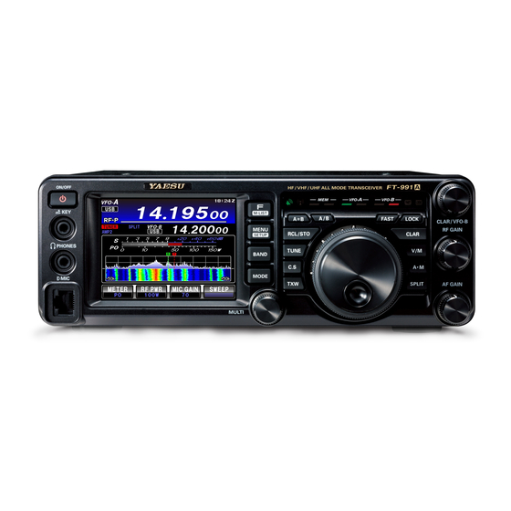
Yaesu FT-991A Technical Supplement
Hf/vhf/uhf all mode transceiver
Hide thumbs
Also See for FT-991A:
- Operating manual (158 pages) ,
- Reference manual (21 pages) ,
- Instruction manual (15 pages)
Table of Contents
Advertisement
Quick Links
HF/VHF/UHF ALL MODE TRANSCEIVER
FT-991
Introduction
This manual provides the technical information necessary
for servicing the FT-991A HF/VHF/UHF ALL MODE
TRANSCEIVER.
Servicing this equipment requires expertise in hand-
ing surface-mount chip components. Attempts by non-
qualified persons to service this equipment may result
in permanent damage not covered by the warranty, and
may be illegal in some countries.
Two PCB layout diagrams provided for each double-
sided board in this transceiver. Each side of the board
is referred to by the type of the majority of components
installed on that side ("Side A" or "Side B"). In most
cases one side has only chip components, and the other
has either a mixture of both chip and leaded components
(trimmers, coils, electrolytic capacitors, ICs, etc.), or
leaded components only.
While we believe the information in this manual to be
correct, YAESU assumes no liability for damage that
may occur as a result of typographical or other errors
that may be present. Your cooperation in pointing out
any inconsistencies in the technical information would
be appreciated.
This transceiver was assembled using Pb (lead) free solder, based on the RoHS specification.
Only lead-free solder (Alloy Composition: Sn-3.0Ag-0.5Cu) should be used for repairs performed on this apparatus. The solder stated
above utilizes the alloy composition required for compliance with the lead-free specification, and any solder with the above alloy com-
position may be used.
Risk of explosion if battery is replaced by an incorrect type. Dispose of used batteries according to the instructions.
Technical Supplement
Exploded View & Miscellaneous Parts
Alignment
Board Unit (Schematics, Layouts & Parts)
MAIN Unit
PLL Unit
EDSP Unit
CNTL Unit
HF-PA Unit
V_U-PA Unit
PANEL Unit
TUNER Unit
JACK Unit
SCP Unit
DSP Unit
Important Note
Caution
EH067M90B
©2017 YAESU MUSEN CO., LTD.
Contents
Advertisement
Table of Contents

Related Manuals for Yaesu FT-991A


Summary of Contents for Yaesu FT-991A
- Page 1 EH067M90B ©2017 YAESU MUSEN CO., LTD. Introduction This manual provides the technical information necessary Contents for servicing the FT-991A HF/VHF/UHF ALL MODE TRANSCEIVER. Specifications Servicing this equipment requires expertise in hand- Exploded View & Miscellaneous Parts ing surface-mount chip components. Attempts by non-...
-
Page 2: Specifications
Specifications General Rx Frequency Range: 30 kHz - 56 MHz, 118 MHz - 164 MHz, 420 MHz - 470 MHz (operating) 1.8 MHz - 54 MHz, 144 MHz - 148 MHz, 430 MHz - 450 MHz (specified performance, Amateur bands only) Tx Frequency Ranges: 1.8 MHz - 54 MHz, 144 MHz - 148 MHz, 430 MHz - 450 MHz (Amateur bands only) - Page 3 Specifications Receiver SSB/CW/AM: Triple-conversion Superheterodyne Circuit Type: FM/C4FM: Double-conversion Superheterodyne Intermediate Frequencies: 40.455 MHz SSB/CW/AM: 69.450 MHz/9.000 MHz/24 kHz FM/C4FM: 69.450 MHz/450 kHz SSB/CW (BW: 2.4 kHz, 10 dB S+N/N) Sensitivity: 0.158 µV (1.8 - 30 MHz) (AMP 2 “ON”) 0.125 µV (50 - 54 MHz) (AMP 2 “ON”) 0.11 µV (144 - 148 MHz) 0.11 µV (430 - 450 MHz)
- Page 4 DOUBLE FACE (19x9) SP 66S-A3627 RA6032300 HEATSINK RA131710A SPONGE RUBBER(SP-CE) RA6046900 BLIND SHEET (0715) RA1550600 SP HOLDER(H034M) REF. YAESU P/N Description Qty. ① U31306007 OVAL HEAD SCREW M3X6B ② U24206001 BIND HEAD TAPTITE-B M2.6X6 ③ U31206007 OVAL HEAD SCREW M2.6X6B ②...
- Page 5 GASKET(70x40) ③ ③ RA0423200 LOCK PLATE RA6000800 SHIELD CASE COVER ③ ③ RA6033500 GASKET (10x20) REF. YAESU P/N Description Qty. ① U31306007 OVAL HEAD SCREW M3X6B ② U20406007 BINDING HEAD SCREW M4X6B ③ U30305002 FLAT HEAD SCREW M3X5NI Non-designated parts are available only as psrt of a designated assembly.
- Page 6 U62009001 VOLUME NUT 9X12X2 RA6107900 FRONT PANEL(PRT) ø2 RA6004600 ø1 KNOB SKIRT ø2 RA6003700 REF. YAESU P/N Description Qty. KNOB ASSY(VOL) ø1 ① U24108001 BIND HEAD TAPTITE-B M2X8(3) ② U24206001 BIND HEAD TAPTITE-B M2.6X6 Non-designated parts are available only as psrt of a designated assembly.
- Page 7 ② ② RA1499500 PORON SHEET(25x35) EDSP-UNIT ② ① ① ② ① ② ① REF. YAESU P/N Description Qty. ① U34206001 FLAT HEAD TAPTITE-B M2.6X6 ② U24206001 BIND HEAD TAPTITE-B M2.6X6 ③ U24208007 BIND HEAD TAPTITE-B M2.6X8B ① Non-designated parts are available only as psrt of a designated assembly.
- Page 8 P1091158A P1090547 (CE ON) ⑥ CONNECTOR CONNECTOR S5000236 (CE ON) LUG WASHER FOR MDR-2 RA6000400 DISPLAY PANEL ⑦ REF. YAESU P/N Description Qty. ① U24206001 BIND HEAD TAPTITE-B M2.6X6 ② U24208007 BIND HEAD TAPTITE-B M2.6X8B ③ U03310002 SEMS SCREW ASM3X10NI ④...
- Page 9 S5000260 LEAD CLAMP CC-1002 ③ TUNER-UNIT ③ RA6015400 GASKET(80x10) RA6025100 Thermal Conductive Pad RA6025200 Thermal Conductive Pad REF. YAESU P/N Description Qty. ① U03306002 PAN HEAD SCREW ASM3X6NI ② U24206001 BIND HEAD TAPTITE-B M2.6X6 ③ U24306001 BIND HEAD TAPTITE-B M3X6 ④...
- Page 10 Block Diagram BLOCK DIAGRAM-1 FT-991 Technical Supplement...
- Page 11 Connection Diagram CONNECTION DIAGRAM-1 FT-991 Technical Supplement...
- Page 12 ANT jack in all proce- dures that call for transmission, except where spec- We recommend that authorized Yaesu Technicians, ified otherwise. Correct alignment is not possible who are experienced with the circuitry and fully with an antenna.
- Page 13 Alignment VDD Meter Adjustment COMP Meter Adjustment Connect the DC voltmeter to J4006 on the HF- Press and hold in the [A=B], [A/B], and [FAST] PA-Unit. keys, while turning the radio on, to enter the Press and hold in the [A=B], [A/B], and [FAST] alignment mode.
- Page 14 Alignment VCO Adjustment Alignment Adjust / DC voltmeter RF millivoltmeter Confirm Menu Item Connect the Digital DC voltmeter (high-Z) to 01-05 VCO1-HIGH Adjust 5.1 V ±0.1 V At least 3 dBm (TXI) L2004 TP2002 on the PLL Unit. Confirm 01-06 VCO1-LOW At least 0.3 V At least 3 dBm...
- Page 15 Alignment 2nd/3rd Local Oscillator Adjustment 3rd Local Level Adjustment Connect the RF millivoltmeter to TP1024 on the Set the VFO-A frequency to 14.200 MHz in the MAIN Unit. CW-USB mode. Adjust T1029 on the MAIN Unit for maximum ...
- Page 16 Alignment REF OSC Adjustment FM Local Oscillator Adjustment Connect the frequency counter to TP1025. Set the FM mode. Press and hold in the [A=B], [A/B], and [FAST] Connect the Digital DC voltmeter (high-Z) keys, while turning the radio on, to enter the TP1008 on the MAIN Unit.
- Page 17 Alignment Press and hold in the [MENU(SETUP)] button 1st Local Oscillator Adjustment for one second to save the new settings and exit Connect the RF millivoltmeter to TP1005 on the the alignment mode. MAIN Unit. Press and hold in the [A=B], [A/B], and [FAST] Alignment RF millivoltmeter Menu Item...
- Page 18 Alignment MCF Adjustment (1) MCF Adjustment (2) Set the VFO-A frequency to 145.900 MHz in the Set the VFO-A frequency to 439.900 MHz in the CW-USB mode. CW-USB mode. Set the following controls as indicated: Set the following controls as indicated: [AGC] : AUTO [AGC] : AUTO [RF GAIN] : Fully clockwise...
- Page 19 Alignment IF Trap Adjustment RF AGC Adjustment Set the VFO-A frequency to 51.900 MHz in the Set the VFO-A frequency to 14.200 MHz in the CW-USB mode. CW-USB mode. Set the following controls as indicated: Set the following controls as indicated: [IPO] : AMP2 [IPO] : AMP1 [ATT] : OFF...
- Page 20 Alignment IF Gain Adjustment Set the following controls as indicated: [IPO] : AMP1 [ATT] : OFF [AGC] : AUTO [RF GAIN] : Fully clockwise Connect the AF millivoltmeter and 4 Ohm dummy load to the EXT SP jack. ...
- Page 21 Alignment S-meter Adjustment S-meter Adjustment (FM) Set the VFO-A frequency to 14.200 MHz in the Set the VFO-A frequency to 145.900 MHz in the USB mode. FM mode. Set the following controls as indicated: Connect the RF Signal Generator to the “144/430 [IPO] : AMP1 MHz”...
- Page 22 Alignment FM Squelch Adjustment FM Center Stop Adjustment Set the VFO-A frequency to 145.900 MHz in the Set the VFO-A frequency to 145.900 MHz in the FM-WIDE mode. FM-WIDE mode. Connect the RF Signal Generator to the “144/430 ...
- Page 23 Alignment Adjust T6501 on the SCP Unit for maximum Scope Adjustment deflection on the SCOPE display. Set the VFO-A frequency to 14.200 MHz in the Turn the RF Signal Generator OFF. CW mode. As shown in the figure below, adjust VR6501 so ...
-
Page 24: Transmitter Adjustment
Alignment Transmitter Adjustment Release the PTT button. Set the VFO-A frequency to 439.900 MHz in the TX IFT Adjustment FM mode. Disconnect the coaxial cable from J1004 on the Press the PTT button, adjust TC1004, TC1003 MAIN Unit, then connect the RF millivoltmeter and TC1002 for maximum deflection on the RF to J1004. - Page 25 Alignment V-U PA Unit Adjustment Pre-Drive Stage Idling Current Adjustment Connect the DC ammeter to J4505 on the V_ Preparation U-PA Unit. Connect the Microphone to the front panel MIC Press and hold the PTT button, while adjust jack.
- Page 26 Alignment Press and hold the PTT button, while adjust Drive Stage Idling Current Adjustment Connect the DC ammeter to J4506 on the V_ VR4503 so the DC ammeter reading is “800 mA U-PA Unit. (±50 mA)”. Release the PTT button. ...
- Page 27 Alignment Press and hold the PTT button, while adjust HF PA Unit Adjustment VR4001 so the DC ammeter reading is “1.5 A Preparation (±0.1 A)”. Connect the Microphone to the front panel MIC Release the PTT button. jack.
- Page 28 Alignment Release the PTT button. CM Coupler Balance Adjustment Connect the 50-Ohm Dummy Load and Watt- Connect the 50-Ohm Dummy Load and Watt- meter to the “HF/50 MHz” ANT jack. meter to the “144/430 MHz” ANT jack. ...
- Page 29 Alignment Rotate the [MULTI] Dial knob to select the Current ALC Adjustment alignment menu item “10-05 I-ALC 50” for the Connect the Microphone to the front panel MIC 50 MHz amateur band's ALC Adjustment. jack. Set the VFO-A frequency to 51.90 MHz in the ...
- Page 30 Alignment ALC Meter Adjustment TX Output Power/PO Meter/TXG Connect the Microphone to the front panel MIC Adjustment jack. Referring to table below, tune the transceiver to C o n n e c t t h e 5 0 - O h m D u m m y L o a d a n d each frequency listed.
- Page 31 Alignment Perform the same procedures for the Alignment Menu Items “11-04 50W FALC 1.8” through “11-15 5W TXG 1.8” per the chart at the below. WAtt AlC m lignment perAtiOn meter meter eter djust tO djust tO djust tO Rotate the [ CLAR/VFO-B ] knob 100 W ( +3 W / -3 W ) 11-01 100W FALC 1.8...
- Page 32 Alignment WAtt AlC m lignment perAtiOn meter meter eter djust tO djust tO djust tO Rotate the [ CLAR/VFO-B ] knob 96 W ( +1 W / -1 W ) 15-01 100W FALC 50 – – Rotate the [ CLAR/VFO-B ] knob 15-02 100W MTR 50 –...
- Page 33 Alignment Connect the 16.6-Ohm Dummy Load and Watt- REV-ALC Adjustment meter to the “144/430 MHz” ANT jack. Connect the 16.6-Ohm Dummy Load and Watt- Rotate the [MULTI] Dial knob to select the meter to the “HF/50 MHz” ANT jack. alignment menu item to “19-06 REV ALC 144".
- Page 34 Alignment Set the VFO-A frequency to 439.90 MHz in the IDD Meter Adjustment C4FM mode. Connect the 50-Ohm Dummy Load and Watt- Press and hold the PTT button, then rotate the meter to the “HF/50 MHz” ANT jack. [CLAR/VFO-B] knob for 4.5 kHz ±0.2 kHz on ...
- Page 35 Alignment Release the PTT button. SWR Meter Adjustment Apply a 4.20 ±0.05 V DC voltage to pin 3 of Set the VFO-A frequency to 1.850 MHz in the J1006, and 2.10 ±0.05 V DC to pin 2 of J1006. USB mode.
-
Page 36: Main Unit
MAIN Unit Circuit Diagram FT-991 Technical Supplement MAIN-1... - Page 37 MAIN Unit Parts Layout (side A) FT-991 Technical Supplement MAIN-2...
- Page 38 MAIN Unit Parts Layout (side B) FT-991 Technical Supplement MAIN-3...
- Page 39 K22174817 C 1073 CHIP CAP. 0.1uF GRM188B11E104KA01D K22144814 C 1074 CHIP CAP. GRM1884C1H2R0BA01D K22174272 C 1075 CHIP CAP. 0.1uF GRM188B11E104KA01D K22144814 C 1076 CHIP CAP. 0.1uF GRM188B11E104KA01D K22144814 FT-99 Technical Supplement ø Please contact YAESU when replacing the MAIN-UNIT. MAIN-4...
- Page 40 MAIN Unit Parts List DESCRIPTION VALUE TOL. MFR'S DESIG YAESU P/N VERS. LOT SIDE LAY ADR C 1077 CHIP CAP. 39pF GRM1882C1H390JA01D K22174225 C 1078 CHIP CAP. 0.1uF GRM188B11E104KA01D K22144814 C 1080 CHIP CAP. 100pF GRM1882C1H101JA01D K22174235 C 1081 CHIP CAP.
- Page 41 MAIN Unit Parts List DESCRIPTION VALUE TOL. MFR'S DESIG YAESU P/N VERS. LOT SIDE LAY ADR C 1158 CHIP CAP. 0.001uF GRM188B11H102KA01D K22174821 C 1159 CHIP CAP. 0.1uF GRM188B11E104KA01D K22144814 C 1160 CHIP CAP. 0.01uF GRM188B11H103KA01D K22174823 C 1161 CHIP TA.CAP.
- Page 42 MAIN Unit Parts List DESCRIPTION VALUE TOL. MFR'S DESIG YAESU P/N VERS. LOT SIDE LAY ADR C 1238 CHIP CAP. GRM1884C1H2R0CA01D K22174203 C 1239 CHIP CAP. 39pF GRM1882C1H390JA01D K22174225 C 1241 CHIP CAP. 22pF GRM1882C1H220JA01D K22174219 C 1242 CHIP CAP.
- Page 43 MAIN Unit Parts List DESCRIPTION VALUE TOL. MFR'S DESIG YAESU P/N VERS. LOT SIDE LAY ADR C 1331 CHIP CAP. 0.01uF GRM188B11H103KA01D K22174823 C 1332 CHIP CAP. 36pF GRM1882C1H360JA01D K22174224 C 1333 CHIP CAP. GRM1882C1H8R0DA01D K22174209 C 1335 CHIP CAP.
- Page 44 MAIN Unit Parts List DESCRIPTION VALUE TOL. MFR'S DESIG YAESU P/N VERS. LOT SIDE LAY ADR C 1432 CHIP CAP. 0.001uF GRM188B11H102KA01D K22174821 C 1433 CHIP CAP. 0.1uF GRM188B11E104KA01D K22144814 C 1434 CHIP CAP. 0.001uF GRM1882C1H102JA01D K22174275 C 1435 CHIP CAP.
- Page 45 MAIN Unit Parts List DESCRIPTION VALUE TOL. MFR'S DESIG YAESU P/N VERS. LOT SIDE LAY ADR C 1507 CHIP CAP. 0.0068uF GRM188B11H682KA01D K22174819 C 1508 CHIP CAP. 0.01uF GRM188B11H103KA01D K22174823 C 1509 CHIP CAP. 0.01uF GRM188B11H103KA01D K22174823 C 1510 CHIP CAP.
- Page 46 MAIN Unit Parts List DESCRIPTION VALUE TOL. MFR'S DESIG YAESU P/N VERS. LOT SIDE LAY ADR C 1588 CHIP CAP. 0.1uF GRM188B11E104KA01D K22144814 C 1590 CHIP CAP. 0.01uF GRM188B11H103KA01D K22174823 C 1591 CHIP CAP. GRM21BB31E105KA98L K22140826 C 1592 CHIP CAP.
- Page 47 MAIN Unit Parts List DESCRIPTION VALUE TOL. MFR'S DESIG YAESU P/N VERS. LOT SIDE LAY ADR C 1668 CHIP CAP. 0.001uF GRM1882C1H102JA01D K22174275 C 1669 CHIP TA.CAP. TMCMA1V105MTRF K78160032 C 1670 CHIP CAP. 0.01uF GRM188B11H103KA01D K22174823 C 1672 CHIP CAP.
- Page 48 MAIN Unit Parts List DESCRIPTION VALUE TOL. MFR'S DESIG YAESU P/N VERS. LOT SIDE LAY ADR C 1748 CHIP CAP. 0.001uF GRM188B11H102KA01D K22174821 C 1749 CHIP CAP. 0.01uF GRM188B11H103KA01D K22174823 C 1750 CHIP TA.CAP. 100uF TMCMC1A107MTRF K78100075 C 1751 CHIP CAP.
- Page 49 MAIN Unit Parts List DESCRIPTION VALUE TOL. MFR'S DESIG YAESU P/N VERS. LOT SIDE LAY ADR C 1837 CHIP CAP. GRM1884C1H2R0BA01D K22174272 C 1838 CHIP CAP. GRM1884C1H2R0CA01D K22174203 C 1841 CHIP CAP. 0.01uF GRM188B11H103KA01D K22174823 C 1843 CHIP CAP. 0.01uF...
- Page 50 MAIN Unit Parts List DESCRIPTION VALUE TOL. MFR'S DESIG YAESU P/N VERS. LOT SIDE LAY ADR D 1001 DIODE EMZ6.8ET2R G2071522 D 1002 SURGE ABSORBER 1608SGXA2-TR2 Q9000891 D 1003 DIODE 1SS302(TE85R.F) G2070088 D 1004 DIODE 1SS372(TE85R.F) G2070632 D 1005 DIODE 1SV281(TPH3.F)
- Page 51 MAIN Unit Parts List DESCRIPTION VALUE TOL. MFR'S DESIG YAESU P/N VERS. LOT SIDE LAY ADR D 1078 DIODE 1SS355 TE-17 G2070470 D 1079 DIODE 1SS355 TE-17 G2070470 D 1080 DIODE 1SS355 TE-17 G2070470 D 1081 DIODE 1SS355 TE-17 G2070470...
- Page 52 MAIN Unit Parts List DESCRIPTION VALUE TOL. MFR'S DESIG YAESU P/N VERS. LOT SIDE LAY ADR FB1042 FERRITE BEADS BLM18BD601SN1D L9190143 FB1043 FERRITE BEADS BLM18BD601SN1D L9190143 FB1044 FERRITE BEADS BLM18BD601SN1D L9190143 FB1045 FERRITE BEADS BLM18BD601SN1D L9190143 FB1046 FERRITE BEADS BLM18BD601SN1D...
- Page 53 MAIN Unit Parts List DESCRIPTION VALUE TOL. MFR'S DESIG YAESU P/N VERS. LOT SIDE LAY ADR L 1018 M.RFC 0.033uH 0603HP-33NXGLW L1691604 L 1019 M.RFC C2012C-1R0J L1691160 L 1020 M.RFC 3.3uH LLM3225-3R3J L1691127 L 1021 M.RFC 3.9uH LLM3225-3R9J L1691128 L 1022 M.RFC...
- Page 54 MAIN Unit Parts List DESCRIPTION VALUE TOL. MFR'S DESIG YAESU P/N VERS. LOT SIDE LAY ADR L 1102 M.RFC 0.12uH LK1608 R12K-T L1690408 L 1103 M.RFC 1000uH LLM3225-102J L1691157 L 1104 FERRITE BEADS BLM18BD182SN1D L1690602 L 1105 FERRITE BEADS BLM18BD182SN1D...
- Page 55 MAIN Unit Parts List DESCRIPTION VALUE TOL. MFR'S DESIG YAESU P/N VERS. LOT SIDE LAY ADR Q 1061 TRANSISTOR 2SB1182-TLQ G3070063 Q 1062 TRANSISTOR 2SC4081 T106 R G3340818R Q 1063 TRANSISTOR DTC114EUA T106 G3070084 Q 1064 TRANSISTOR 2SC4081 T106 R...
- Page 56 MAIN Unit Parts List DESCRIPTION VALUE TOL. MFR'S DESIG YAESU P/N VERS. LOT SIDE LAY ADR Q 1152 TRANSISTOR 2SA1576A T106 R G3115768R Q 1153 TRANSISTOR 2SC4081 T106 R G3340818R Q 1154 NJM2594V-TE1 G1093750 Q 1155 TRANSISTOR DTC114EUA T106 G3070084...
- Page 57 MAIN Unit Parts List DESCRIPTION VALUE TOL. MFR'S DESIG YAESU P/N VERS. LOT SIDE LAY ADR R 1051 CHIP RES. 100k 1/16W RMC1/16 104JATP J24185104 R 1052 CHIP RES. 1/16W RMC1/16 101JATP J24185101 R 1053 CHIP RES. 1/16W RMC1/16 101JATP...
- Page 58 MAIN Unit Parts List DESCRIPTION VALUE TOL. MFR'S DESIG YAESU P/N VERS. LOT SIDE LAY ADR R 1126 CHIP RES. 1/16W RMC1/16 330JATP J24185330 R 1127 CHIP RES. 1/16W RMC1/16 103JATP J24185103 R 1128 CHIP RES. 1/16W RMC1/16 683JATP J24185683 R 1129 CHIP RES.
- Page 59 MAIN Unit Parts List DESCRIPTION VALUE TOL. MFR'S DESIG YAESU P/N VERS. LOT SIDE LAY ADR R 1215 CHIP RES. 1/16W RMC1/16 223FTP J24183223 R 1216 CHIP RES. 1/16W RMC1/16 101JATP J24185101 R 1217 CHIP RES. 1/16W RMC1/16 101JATP J24185101 R 1218 CHIP RES.
- Page 60 MAIN Unit Parts List DESCRIPTION VALUE TOL. MFR'S DESIG YAESU P/N VERS. LOT SIDE LAY ADR R 1305 CHIP RES. 1/16W RMC1/16 103JATP J24185103 R 1306 CHIP RES. 100k 1/16W RMC1/16 104FTP J24183104 R 1307 CHIP RES. 1/16W RMC1/16 223JATP...
- Page 61 MAIN Unit Parts List DESCRIPTION VALUE TOL. MFR'S DESIG YAESU P/N VERS. LOT SIDE LAY ADR R 1381 CHIP RES. 6.8k 1/16W RMC1/16 682JATP J24185682 R 1382 CHIP RES. 1/16W RMC1/16 103JATP J24185103 R 1383 CHIP RES. 470k 1/16W RMC1/16 474JATP...
- Page 62 MAIN Unit Parts List DESCRIPTION VALUE TOL. MFR'S DESIG YAESU P/N VERS. LOT SIDE LAY ADR R 1460 CHIP RES. 4.7k 1/16W RMC1/16 472JATP J24185472 R 1461 CHIP RES. 1/16W RMC1/16 153JATP J24185153 R 1462 CHIP RES. 100k 1/16W RMC1/16 104JATP...
- Page 63 MAIN Unit Parts List DESCRIPTION VALUE TOL. MFR'S DESIG YAESU P/N VERS. LOT SIDE LAY ADR R 1537 CHIP RES. 1/16W RMC1/16 103JATP J24185103 R 1538 CHIP RES. 1/16W RMC1/16 101JATP J24185101 R 1539 CHIP RES. 2.2M 1/16W RMC1/16 225JATP...
- Page 64 MAIN Unit Parts List DESCRIPTION VALUE TOL. MFR'S DESIG YAESU P/N VERS. LOT SIDE LAY ADR R 1616 CHIP RES. 1/16W RMC1/16 221JATP J24185221 R 1617 CHIP RES. 1/10W RMC1/10T 000J J24205000 R 1618 CHIP RES. 150k 1/16W RMC1/16 154JATP...
- Page 65 MAIN Unit Parts List DESCRIPTION VALUE TOL. MFR'S DESIG YAESU P/N VERS. LOT SIDE LAY ADR R 1696 CHIP RES. 1/16W RMC1/16 470JATP J24185470 R 1697 CHIP RES. 1/16W RMC1/16 470JATP J24185470 R 1698 CHIP RES. 1/16W RMC1/16 470JATP J24185470 R 1701 CHIP RES.
- Page 66 MAIN Unit Parts List DESCRIPTION VALUE TOL. MFR'S DESIG YAESU P/N VERS. LOT SIDE LAY ADR R 1796 CHIP RES. 1/16W RMC1/16 333FTP J24183333 R 1797 CHIP RES. 1/16W RMC1/16 221JATP J24185221 R 1798 CHIP RES. 1/16W RMC1/16 101JATP J24185101 R 1800 CHIP RES.
- Page 67 MAIN Unit Parts List DESCRIPTION VALUE TOL. MFR'S DESIG YAESU P/N VERS. LOT SIDE LAY ADR SHIELD CASE (28x15) RA1152200 SHIELD CASE COVER (28x15) RA1152300 SHIELD PLATE RA6002100 SHIELD CASE (21X25.5) RA6110000 FT-99 Technical Supplement MAIN-32...
-
Page 68: Pll Unit
PLL Unit Circuit Diagram FT-991 Technical Supplement PLL-1... - Page 69 PLL Unit Parts Layout side A side B FT-991 Technical Supplement PLL-2...
- Page 70 PLL Unit Parts List DESCRIPTION VALUE TOL. MFR'S DESIG YAESU P/N VERS. LOT SIDE LAY ADR PCB with Components CS2469601 C 2001 CHIP CAP. 0.001uF GRM1882C1H102JA01D K22174275 C 2002 CHIP CAP. 0.001uF GRM1882C1H102JA01D K22174275 C 2003 CHIP CAP. 0.001uF GRM1882C1H102JA01D...
- Page 71 PLL Unit Parts List DESCRIPTION VALUE TOL. MFR'S DESIG YAESU P/N VERS. LOT SIDE LAY ADR C 2085 CHIP CAP. 0.1uF GRM188B11E104KA01D K22144814 C 2086 CHIP CAP. 0.1uF GRM188B11E104KA01D K22144814 C 2087 CHIP CAP. 0.001uF GRM188B11H102KA01D K22174821 C 2088 CHIP CAP.
- Page 72 PLL Unit Parts List DESCRIPTION VALUE TOL. MFR'S DESIG YAESU P/N VERS. LOT SIDE LAY ADR Q 2005 MCH3914-7-TL-H G3070439 Q 2006 MCH3914-7-TL-H G3070439 Q 2007 MCH3914-7-TL-H G3070439 Q 2008 TRANSISTOR DTC124EUA T106 G3070045 Q 2009 TRANSISTOR DTC124EUA T106 G3070045...
- Page 73 EDSP Unit Circuit Diagram FT-991 Technical Supplement EDSP-1...
- Page 74 EDSP Unit Parts Layout side A side B FT-991 Technical Supplement EDSP-2...
- Page 75 EDSP Unit Parts List DESCRIPTION VALUE TOL. MFR'S DESIG YAESU P/N VERS. LOT SIDE LAY ADR PCB with Components CS2470701 C 2511 CHIP CAP. 0.001uF GRM155B11H102KA01D K22178809 C 2514 CHIP CAP. 10uF GRM188R61E106MA73D K22144818 C 2515 CHIP CAP. 22pF GRM1552C1H220JA01D...
- Page 76 EDSP Unit Parts List DESCRIPTION VALUE TOL. MFR'S DESIG YAESU P/N VERS. LOT SIDE LAY ADR C 2593 CHIP CAP. 0.47uF 6.3V GRM155B30J474KE18D K22088802 C 2594 CHIP CAP. 0.47uF 6.3V GRM155B30J474KE18D K22088802 C 2595 CHIP CAP. 0.47uF 6.3V GRM155B30J474KE18D K22088802 C 2596 CHIP CAP.
- Page 77 EDSP Unit Parts List DESCRIPTION VALUE TOL. MFR'S DESIG YAESU P/N VERS. LOT SIDE LAY ADR R 2503 CHIP RES. 1/16W RMC1/16S 103JTH J24189037 R 2504 CHIP RES. 1/16W RMC1/16S 103JTH J24189037 R 2505 CHIP RES. 2.2k 1/16W RMC1/16S 222JTH...
- Page 78 EDSP Unit Parts List DESCRIPTION VALUE TOL. MFR'S DESIG YAESU P/N VERS. LOT SIDE LAY ADR R 2590 CHIP RES. 1/16W RMC1/16S 330JTH J24189007 R 2591 CHIP RES. 1/16W RMC1/16S 330JTH J24189007 R 2592 CHIP RES. 1/16W RMC1/16S 330JTH J24189007 R 2593 CHIP RES.
-
Page 79: Cntl Unit
CNTL Unit Circuit Diagram FT-991 Technical Supplement CNTL-1... - Page 80 CNTL Unit Parts Layout (side A) FT-991 Technical Supplement CNTL-2...
- Page 81 CNTL Unit Parts Layout (side B) FT-991 Technical Supplement CNTL-3...
- Page 82 C 3081 CHIP CAP. 0.1uF GRM155B11A104KA01D K22108802 C 3082 CHIP CAP. 0.1uF GRM155B11A104KA01D K22108802 C 3083 CHIP CAP. 0.001uF GRM155B11H102KA01D K22178809 C 3084 CHIP CAP. 0.01uF GRM155B11E103KA01D K22148834 FT-99 Technical Supplement ø Please contact YAESU when replacing the CNTL-UNIT. CNTL-4...
- Page 83 Q 3027 CD74HC238PWR G1094275 Q 3028 CD74HC238PWR G1094275 Q 3029 CD74HC238PWR G1094275 Q 3030 CD74HC238PWR G1094275 Q 3032 LM2904PWR G1094010 Q 3033 SN74LVC3G17DCTR G1094419 Q 3034 SN74LVC3G17DCTR G1094419 FT-99 Technical Supplement ø Please contact YAESU when replacing this part. CNTL-5...
- Page 84 CNTL Unit Parts List DESCRIPTION VALUE TOL. MFR'S DESIG YAESU P/N VERS. LOT SIDE LAY ADR Q 3035 LM2904PWR G1094010 Q 3037 TRANSISTOR DTC114YUA T106 G3070298 Q 3038 TRANSISTOR DTC114YUA T106 G3070298 Q 3039 POLY SWITCH NANOSMDC035F(TAPE) G9090167 R 3003 CHIP RES.
- Page 85 CNTL Unit Parts List DESCRIPTION VALUE TOL. MFR'S DESIG YAESU P/N VERS. LOT SIDE LAY ADR R 3086 CHIP RES. 1/16W RMC1/16S 223JTH J24189041 R 3087 CHIP RES. 1/16W RMC1/16S 223JTH J24189041 R 3088 CHIP RES. 1/16W RMC1/16S 102JTH J24189025 R 3089 CHIP RES.
- Page 86 CNTL Unit Parts List DESCRIPTION VALUE TOL. MFR'S DESIG YAESU P/N VERS. LOT SIDE LAY ADR R 3164 CHIP RES. 1/16W RMC1/16S JPTH J24189070 R 3165 CHIP RES. 1/16W RMC1/16S JPTH J24189070 R 3170 CHIP RES. 100k 1/16W RMC1/16S 104JTH...
- Page 87 HF-PA Unit Circuit Diagram FT-991 Technical Supplement HF-PA-1...
- Page 88 HF-PA Unit Parts Layout (side A) FT-991 Technical Supplement HF-PA-2...
- Page 89 HF-PA Unit Parts Layout (side B) FT-991 Technical Supplement HF-PA-3...
- Page 90 HF-PA Unit Parts List DESCRIPTION VALUE TOL. MFR'S DESIG YAESU P/N VERS. LOT SIDE LAY ADR PCB with Components CS2471601 C 4007 CHIP CAP. 0.1uF GRM188B11E104KA01D K22144814 C 4013 CHIP CAP. 0.1uF GRM188B11E104KA01D K22144814 C 4022 CHIP CAP. 0.01uF GRM188B11H103KA01D...
- Page 91 HF-PA Unit Parts List DESCRIPTION VALUE TOL. MFR'S DESIG YAESU P/N VERS. LOT SIDE LAY ADR C 4130 CHIP CAP. 0.01uF GRM188B11H103KA01D K22174823 C 4131 FILM CAP. 220pF 500V UC342H2200J-T K33279011 C 4132 CHIP CAP. 0.01uF GRM188B11H103KA01D K22174823 C 4133 FILM CAP.
- Page 92 HF-PA Unit Parts List DESCRIPTION VALUE TOL. MFR'S DESIG YAESU P/N VERS. LOT SIDE LAY ADR C 4228 CHIP CAP. 18pF 250V GRM21A5C2E180JW01D K22240304 C 4230 CHIP CAP. 470pF 250V GRM21A7U2E471JW31D K22240321 C 4231 CHIP CAP. 47pF 250V GRM21A5C2E470JW01D K22240309 C 4232 CHIP CAP.
- Page 93 HF-PA Unit Parts List DESCRIPTION VALUE TOL. MFR'S DESIG YAESU P/N VERS. LOT SIDE LAY ADR D 4031 DIODE RB551V-30 TE-17 G2070892 D 4032 DIODE RB551V-30 TE-17 G2070892 D 4033 DIODE RB551V-30 TE-17 G2070892 FB4001 RFC WITH BEADS 3A RI5.8X6.4-2...
- Page 94 HF-PA Unit Parts List DESCRIPTION VALUE TOL. MFR'S DESIG YAESU P/N VERS. LOT SIDE LAY ADR Q 4027 TRANSISTOR UMD5N TR G3070343 Q 4029 TA75S01F(TE85R.F) G1091593 Q 4030 SN74LVC2G53DCTR G1094048 Q 4032 LM2902PWR G1094009 R 4001 CHIP RES. 3.9k 1/16W...
- Page 95 HF-PA Unit Parts List DESCRIPTION VALUE TOL. MFR'S DESIG YAESU P/N VERS. LOT SIDE LAY ADR R 4085 CHIP RES. 1/16W RMC1/16 470JATP J24185470 R 4086 CHIP RES. 1/16W RMC1/16 470JATP J24185470 R 4087 CHIP RES. RMC1 560JTE J24305560 R 4088 CHIP RES.
- Page 96 V_U-PA Unit Circuit Diagram FT-991 Technical Supplement V_U-PA-1...
- Page 97 V_U-PA Unit Parts Layout (side A) FT-991 Technical Supplement V_U-PA-2...
- Page 98 V_U-PA Unit Parts Layout (side B) FT-991 Technical Supplement V_U-PA-3...
- Page 99 V_U-PA Unit Parts List DESCRIPTION VALUE TOL. MFR'S DESIG YAESU P/N VERS. LOT SIDE LAY ADR PCB with Components CS2466601 C 4501 AL.ELECTRO.CAP. 47uF EEE1VA470WP K48160005 C 4502 CHIP CAP. 10uF GRM31CB31E106KA75L K22141815 C 4506 CHIP CAP. 0.001uF GRM188B11H102KA01D K22174821 C 4507 CHIP CAP.
- Page 100 V_U-PA Unit Parts List DESCRIPTION VALUE TOL. MFR'S DESIG YAESU P/N VERS. LOT SIDE LAY ADR C 4597 CHIP CAP. 100pF GRM1882C1H101JA01D K22174235 C 4598 CHIP CAP. 100pF GRM1882C1H101JA01D K22174235 C 4599 CHIP CAP. 100pF GRM1882C1H101JA01D K22174235 C 4600 AL.ELECTRO.CAP.
- Page 101 V_U-PA Unit Parts List DESCRIPTION VALUE TOL. MFR'S DESIG YAESU P/N VERS. LOT SIDE LAY ADR C 4695 CHIP CAP. 10pF 250V GRM21A5C2E100JW01D K22240301 C 4697 CHIP CAP. 250V GQM1875C2E4R0CB12D K22244212 C 4698 CHIP CAP. 0.001uF GRM188B11H102KA01D K22174821 C 4699 CHIP CAP.
- Page 102 V_U-PA Unit Parts List DESCRIPTION VALUE TOL. MFR'S DESIG YAESU P/N VERS. LOT SIDE LAY ADR J 4503 TERMINAL Y106 S5000179 J 4504 TERMINAL Y106 S5000179 J 4505 CONNECTOR IMSA-9202B-1-02-T P0091174 J 4506 CONNECTOR IMSA-9202B-1-02-T P0091174 J 4507 CONNECTOR IMSA-9202B-1-02-T...
- Page 103 V_U-PA Unit Parts List DESCRIPTION VALUE TOL. MFR'S DESIG YAESU P/N VERS. LOT SIDE LAY ADR R 4505 CHIP RES. RMC1 6R8JTE J24305689 R 4506 CHIP RES. 1/16W RMC1/16 390JATP J24185390 R 4507 CHIP RES. 1/16W RMC1/16 390JATP J24185390 R 4508 CHIP RES.
- Page 104 V_U-PA Unit Parts List DESCRIPTION VALUE TOL. MFR'S DESIG YAESU P/N VERS. LOT SIDE LAY ADR R 4591 CHIP RES. RMC1 JPATE J24305000 R 4592 CHIP RES. 5.6k 1/16W RMC1/16 562JATP J24185562 R 4593 CHIP RES. 8.2k 1/16W RMC1/16 822JATP...
-
Page 105: Panel Unit
PANEL Unit Circuit Diagram FT-991 Technical Supplement PANEL-1... - Page 106 PANEL Unit Parts Layout side A side B FT-991 Technical Supplement PANEL-2...
- Page 107 PANEL Unit Parts List DESCRIPTION VALUE TOL. MFR'S DESIG YAESU P/N VERS. LOT SIDE LAY ADR PCB with Components CS2472601 BT5501 LITHIUM BATT. ML614R-TT31 Q9000895 C 5501 CHIP CAP. 0.0047uF GRM155B11H472KA01D K22178838 C 5502 CHIP CAP. 10uF GRM21BB31A106KE18L K22100808 C 5503 CHIP CAP.
- Page 108 PANEL Unit Parts List DESCRIPTION VALUE TOL. MFR'S DESIG YAESU P/N VERS. LOT SIDE LAY ADR C 5579 CHIP CAP. 0.1uF GRM155B11A104KA01D K22108802 C 5580 CHIP CAP. 0.001uF GRM155B11H102KA01D K22178809 C 5582 CHIP CAP. 0.1uF GRM155B11A104KA01D K22108802 C 5583 CHIP CAP.
- Page 109 PANEL Unit Parts List DESCRIPTION VALUE TOL. MFR'S DESIG YAESU P/N VERS. LOT SIDE LAY ADR C 5662 CHIP CAP. 0.1uF GRM155B11A104KA01D K22108802 C 5663 CHIP CAP. 0.1uF GRM155B11A104KA01D K22108802 C 5664 CHIP CAP. 0.001uF GRM155B11H102KA01D K22178809 C 5665 CHIP TA.CAP.
- Page 110 PANEL Unit Parts List DESCRIPTION VALUE TOL. MFR'S DESIG YAESU P/N VERS. LOT SIDE LAY ADR FB5522 FERRITE BEADS BK2125HS601-T L9190085 J 5501 CONNECTOR 9617S-04 P1091433 J 5502 CONNECTOR 9637S-50A P1091434 J 5503 CONNECTOR SB20-04WS P0090611 J 5504 CONNECTOR 12FLT-SM2-TB(LF)(SN)
- Page 111 PANEL Unit Parts List DESCRIPTION VALUE TOL. MFR'S DESIG YAESU P/N VERS. LOT SIDE LAY ADR R 5543 CHIP RES. 1/16W RMC1/16S 105JTH J24189061 R 5544 CHIP RES. 1/16W RMC1/16S 103JTH J24189037 R 5545 CHIP RES. 1/16W RMC1/16S 103JTH J24189037 R 5546 CHIP RES.
- Page 112 PANEL Unit Parts List DESCRIPTION VALUE TOL. MFR'S DESIG YAESU P/N VERS. LOT SIDE LAY ADR R 5624 CHIP RES. 1/16W RMC1/16S JPTH J24189070 R 5625 CHIP RES. 3.3k 1/16W RMC1/16S 332JTH J24189031 R 5626 CHIP RES. 1/16W RMC1/16S 473JTH...
-
Page 113: Tuner Unit
TUNER Unit Circuit Diagram FT-991 Technical Supplement TUNER-1... - Page 114 TUNER Unit Parts Layout (side A) FT-991 Technical Supplement TUNER-2...
- Page 115 TUNER Unit Parts Layout (side B) FT-991 Technical Supplement TUNER-3...
- Page 116 TUNER Unit Parts List DESCRIPTION VALUE TOL. MFR'S DESIG YAESU P/N VERS. LOT SIDE LAY ADR PCB with Components CS2467701 C 6001 CHIP CAP. 0.1uF GRM188B11E104KA01D K22144814 C 6002 CHIP CAP. 0.1uF GRM188B11E104KA01D K22144814 C 6003 CHIP CAP. 0.1uF GRM188B11E104KA01D...
- Page 117 TUNER Unit Parts List DESCRIPTION VALUE TOL. MFR'S DESIG YAESU P/N VERS. LOT SIDE LAY ADR D 6018 DIODE BAS316 G2070716 D 6019 DIODE BAS316 G2070716 D 6020 DIODE BAS316 G2070716 D 6021 DIODE BAS316 G2070716 D 6022 DIODE BAS316...
- Page 118 TUNER Unit Parts List DESCRIPTION VALUE TOL. MFR'S DESIG YAESU P/N VERS. LOT SIDE LAY ADR RL6001 RELAY FTR-F3AA012E-(F) M1190224 RL6002 RELAY FTR-F3AA012E-(F) M1190224 RL6003 RELAY FTR-F3AA012E-(F) M1190224 RL6004 RELAY FTR-F3AA012E-(F) M1190224 RL6005 RELAY FTR-F3AA012E-(F) M1190224 RL6006 RELAY FTR-F3AA012E-(F) M1190224...
- Page 119 JACK Unit Circuit Diagram FT-991 Technical Supplement JACK-1...
- Page 120 JACK Unit Parts Layout side A side B FT-991 Technical Supplement JACK-2...
- Page 121 JACK Unit Parts List DESCRIPTION VALUE TOL. MFR'S DESIG YAESU P/N VERS. LOT SIDE LAY ADR PCB with Components CD0378001 C 7002 CHIP CAP. 0.001uF GRM188B11H102KA01D K22174821 C 7007 CHIP CAP. 0.001uF GRM188B11H102KA01D K22174821 C 7008 CHIP CAP. 0.001uF GRM188B11H102KA01D...
- Page 122 SCP Unit Circuit Diagram FT-991 Technical Supplement SCP-1...
- Page 123 SCP Unit Parts Layout side A side B FT-991 Technical Supplement SCP-2...
- Page 124 SCP Unit Parts List DESCRIPTION VALUE TOL. MFR'S DESIG YAESU P/N VERS. LOT SIDE LAY ADR PCB with Components CD0379001 C 6501 CHIP CAP. 51pF GRM1882C1H510JA01D K22174228 C 6502 CHIP CAP. GRM1882C1H4R0CA01D K22174205 C 6502 CHIP CAP. 68pF GRM1882C1H680JA01D K22174231 C 6503 CHIP CAP.
- Page 125 SCP Unit Parts List DESCRIPTION VALUE TOL. MFR'S DESIG YAESU P/N VERS. LOT SIDE LAY ADR C 6576 CHIP CAP. 470pF GRM1882C1H471JA01D K22174249 C 6577 CHIP CAP. 220pF GRM1882C1H221JA01D K22174243 C 6578 CHIP CAP. 82pF GRM1882C1H820JA01D K22174233 C 6579 CHIP CAP.
- Page 126 SCP Unit Parts List DESCRIPTION VALUE TOL. MFR'S DESIG YAESU P/N VERS. LOT SIDE LAY ADR R 6535 CHIP RES. 2.2k 1/16W RMC1/16 222JATP J24185222 R 6536 CHIP RES. 1/16W RMC1/16 101JATP J24185101 R 6537 CHIP RES. 4.7k 1/16W RMC1/16 472JATP...
-
Page 127: Dsp Unit
DSP Unit Circuit Diagram FT-991 Technical Supplement DSP-1... - Page 128 DSP Unit Parts Layout side B side A FT-991 Technical Supplement DSP-2...
- Page 129 DSP Unit Parts List DESCRIPTION VALUE TOL. MFR'S DESIG YAESU P/N VERS. LOT SIDE LAY ADR PCB with Components CS2465501 C 9003 CHIP CAP. 220pF GRM155B11H221KA01D K22178801 C 9005 CHIP CAP. 0.1uF GRM155B11A104KA01D K22108802 C 9006 CHIP CAP. 0.0082uF GRM155B11C822KA01D...
- Page 130 DSP Unit Parts List DESCRIPTION VALUE TOL. MFR'S DESIG YAESU P/N VERS. LOT SIDE LAY ADR R 9038 CHIP RES. 1/16W RMC1/16S JPTH J24189070 R 9039 CHIP RES. 1/16W RMC1/16S JPTH J24189070 R 9040 CHIP RES. 1/16W RMC1/16S 103JTH J24189037 R 9041 CHIP RES.
- Page 131 Copyright 2017 YAESU MUSEN CO., LTD. All rights reserved No portion of this manual may be reproduced without the permission of YAESU MUSEN CO., LTD.
Need help?
Do you have a question about the FT-991A and is the answer not in the manual?
Questions and answers
why can't I log into fusion with my 991a no matter what i try. I have tried 5 repeaters that say they are fusion enabled. All I get is a "beep" search and fter 10 seconds, "failed." Help'