Table of Contents
Advertisement
Quick Links
Download this manual
See also:
User Manual
Advertisement
Table of Contents

Related Manuals for Lumistar LS-28-DRSM


Summary of Contents for Lumistar LS-28-DRSM
- Page 1 LS-28-DRSM Interface Control Document 5/2/2019 LS-28-DRSM Multi-Mode Modular Receiver Interface Control Document (ICD) Lumistar Inc 2270 Camino Vida Roble, Suite L Carlsbad, California 92011 (760) 431-2181 www.lumistar.net Lumistar Inc. DOC-28M-01-ICD-07...
- Page 2 Lumistar, Inc. This document is provided as is, with no warranties of any kind. Lumistar, Inc. disclaims and excludes all other warranties and product liability, expressed or implied, including but not limited to any implied...
- Page 3 LS-28-DRSM Interface Control Document 5/2/2019 Table of Contents DOCUMENT INTRODUCTION ......................... 15 .................................15 ANUAL ORMAT ................................15 OCUMENT ABELS DOCUMENT INTRODUCTION ......................... 16 DEVICE INTERFACES ..........................21 TCP COMMAND/STATUS MESSAGE DEFINITIONS ................25 4.1.1 P 0000 ..............................25 OMMAND 4.2.1 S 1000 ....................26...
- Page 4 LS-28-DRSM Interface Control Document 5/2/2019 4.3.9 D 1108 .........................68 ECOMMUTATOR ETUP OMMAND 4.3.10 D 1109 ................70 ECOMMUTATOR TTRIBUTES ETUP OMMAND 4.3.11 LDPC D 110A ..................73 ATTERN ETUP OMMAND 4.3.12 LDPC D 110C ........................75 ECODER ETUP OMMAND 4.3.13 LDPC D 110D ....................77...
- Page 5 LS-28-DRSM Interface Control Document 5/2/2019 4.8.6 D 210A ..................142 TREAM ATTERN TATUS ESSAGE 4.8.7 LDPC D 210C ......................... 143 ECODER TATUS ESSAGE 4.8.8 LDPC E 2113 ......................... 145 NCODER TATUS ESSAGE 4.9.1 C PSK S 4100 ..................147 URRENT...
- Page 6 LS-28-DRSM Interface Control Document 5/2/2019 5.2.2.2 C – P 1 ................210 ONSOLIDATED TATUS ESSAGE ONTENT AYLOAD NDEX 5.2.2.3 C – P 2 ................211 ONSOLIDATED TATUS ESSAGE ONTENT AYLOAD NDEX 5.2.2.4 C – P 3 ................212 ONSOLIDATED TATUS...
-
Page 7: Table Of Contents
LS-28-DRSM Interface Control Document 5/2/2019 List of Figures Figure 1-1 Document Flag Formats ............................15 Figure 2-1 Block Diagram: Slice 1 - RF to IF Downconversion..................18 Figure 2-2 Block Diagram: Slice 2 - 2 IF and Analog Processing ................19 Figure 2-3 Block Diagram: Slice 3 - Digital Signal Processing .................. - Page 8 LS-28-DRSM Interface Control Document 5/2/2019 Figure 4-39 Start or Stop NAND Flash File Recording Response Message 0x1010 ..........50 Figure 4-40 NAND Flash Monitor Command/Status Message 0x1011 ..............51 Figure 4-41 NAND (Recording) Flash Download File Command Message 0x1012 ..........52 Figure 4-42 NAND Flash (Rec.
- Page 9 LS-28-DRSM Interface Control Document 5/2/2019 Figure 4-87 PCM/FM Combiner Setup Command Message 0x1205 ................89 Figure 4-88 PCM/FM Combiner Setup Response Message 0x1205 ................90 Figure 4-89 PCMFM Receiver Demodulator Setup Command Message 0x120E ........... 90 Figure 4-90 PCMFM Receiver PCM Output Encoder Selections ................... 91 Figure 4-91 PCMFM Receiver Demodulator Setup Response Message 0x120E .............
- Page 10 LS-28-DRSM Interface Control Document 5/2/2019 Figure 4-135 LDPC Decoder Status Command Message 0x210C................143 Figure 4-136 LDPC Decoder Status Response Message 0x210C ................144 Figure 4-137 LDPC Encoder Status Command Message 0x2113 ................145 Figure 4-138 LDPC Encoder Status Response Message 0x2113 ................. 146 Figure 4-139 Current Primary PSK Setup Status Command Message 0x4100 ............
- Page 11 LS-28-DRSM Interface Control Document 5/2/2019 Figure 4-183 Current Secondary Bit Sync Setup Status Response Message 0x4401 .......... 184 Figure 4-184 Current Sec Bit Sync Output Encoder Selection Table ................. 185 Figure 5-1 Graphing UDP Datagram Header Contents ....................186 Figure 5-2 Data Packet Transfer Case Definitions ......................223 Figure 5-3 Example of real-time streaming package set (SOY) ...................
- Page 12 LS-28-DRSM Interface Control Document 5/2/2019 List of Tables Table 2-1 General Device Specifications Table ........................17 Table 3-1 Ethernet Port Assignments Table .......................... 22 Table 4-1 0x1000 Set Receiver Operational Mode Command Message Bits Definitions........26 Table 4-2 0x1001 Command Message Bit Definitions ...................... 27 Table 4-3 0x1002 Continuious UDP Data Request Message Bit Definitions ............
- Page 13 LS-28-DRSM Interface Control Document 5/2/2019 Table 4-44 0x1112 TX PCM Encoder Setup Command Message Bit Definitions ............ 80 Table 4-45 0x1113 LDPC Encoder Setup Command Message Bit Definitions ............82 Table 4-46 0x1200 PCM/FM Receiver Setup Command Message Bit Definitions ..........85 Table 4-47 0x1200 PCM/FM Receiver Setup Status Response Message Bit Definitions ........
- Page 14 LS-28-DRSM Interface Control Document 5/2/2019 Table 4-92 0x4108 Current Decommutator Setup Command Message Bit Definitions ........162 Table 4-93 0x4108 Current Decommutator Setup Response Message Bit Definitions........163 Table 4-94 0x410A Dual Length FSync Pattern Setup Response Message Bit Definitions ....... 165 Table 4-95 Current LDPC Decoder Pri.
-
Page 15: Figure 1-1 Document Flag Formats
1. Document Introduction 1.1 General This document provides the communications interface definitions for the LS-28-DRSM product line. It defines the message formats and protocols for controlling and statusing the device via one of its interface methods. From this point forward this document will simply be referred to as the Interface Control Document (ICD). - Page 16 The unit has been designed in such a manner that precludes the necessity of a commercial operating system hosted within the device. The LS-28-DRSM is capable of many functions in the signal processing and post processing arena. Please refer to the device sales literature for full details on available options and capabilities.
-
Page 17: Table 2-1 General Device Specifications Table
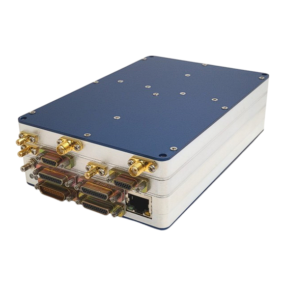
LS-28-DRSM Interface Control Document 5/2/2019 Category: Specifications: Details: Mechanical Envelope Dimensions (all slices) 6.00”(L) x 4.00”(W) x 1.672” (H) - PCI Form Factor Modular Brick Weight ~ 32oz. Electrical Individual power requirements 9-42VDC Nom. +24VDC @ 2.875A Total Power (both Channels) -
Page 18: Figure 2-1 Block Diagram: Slice 1 - Rf To If Downconversion
LS-28-DRSM Interface Control Document 5/2/2019 Figure 2-1 Block Diagram: Slice 1 - RF to IF Downconversion Lumistar Inc. DOC-28M-01-ICD-07... -
Page 19: Figure 2-2 Block Diagram: Slice 2 - 2 Nd If And Analog Processing
LS-28-DRSM Interface Control Document 5/2/2019 Figure 2-2 Block Diagram: Slice 2 - 2 IF and Analog Processing Figure 2-3 Block Diagram: Slice 3 - Digital Signal Processing Lumistar Inc. DOC-28M-01-ICD-07... -
Page 20: Figure 2-4 Block Diagram: Slice 4 - Processing, Storage And Dc Power Conversion
LS-28-DRSM Interface Control Document 5/2/2019 Figure 2-4 Block Diagram: Slice 4 – Processing, Storage and DC Power Conversion Lumistar Inc. DOC-28M-01-ICD-07... -
Page 21: Figure 3-1 Interface Capabilities Matrix
921.6K BAUD rates. 3.2 USB 2.0 Interface The LS-28-DRSM provides a USB 2.0 serial interface. Included with the delivery is a driver installation that converts the USB serial interface into a standard COM port for a number of different operating systems, Lumistar Inc. -
Page 22: Table 3-1 Ethernet Port Assignments Table
1 start bit, 1 stop bit and no parity. The speed can be increased dramatically to a maximum of 921.6K BAUD. This interface is capable of being used for field upgrade of on-board firmware sources. 3.3 Ethernet Interface The LS-28-DRSM provides a 10/100/1000Mbps Ethernet interface. This interface is considered the “primary”, and most capable, device interface. -
Page 23: Figure 3-2 General Message Structure
LS-28-DRSM Interface Control Document 5/2/2019 Figure 3-2 General Message Structure The message structure is applied to both the command and the response. The op code is typically arranged on a “series” basis and is grouped with similar functional messages. For example, the most primitive message supported is the device “Ping”... - Page 24 These protocol extensions and definitions are beyond the scope of this manual. Refer to appropriate networking documentation for additional information. Ethernet package payload sizes are limited to 1500 bytes for the LS-28-DRSM and follow the IEEE 802.3 format.
-
Page 25: Figure 4-1 Ping Series 0X0000 Command And Response Message
This series of messages is for primary interface identification and test. Only one message exists in this series of messages as defined below. This ping message is provided in all LS-28-DRSM configurations. Refer to Figure 4-1 for command and status response message formats. -
Page 26: Figure 4-2 Set Receiver Operational Mode Command Message
This series of commands are primary functional commands which are used for setting operational modes. See definitions below. This series of messages are provided in all LS-28-DRSM configurations regardless of licensing of functional options. Refer to Figure 4-2 for the Operational Mode Command definition. -
Page 27: Figure 4-4 Mode Command Message 0X1001
LS-28-DRSM Interface Control Document 5/2/2019 4.2.2 Mode Command Message 0x1001 Figure 4-4 Mode Command Message 0x1001 The mode command message is not to be confused with the 0x1000 series operational mode command. This message provides a means of performing discrete utilitarian tasks. Some of these tasks provide the user with configuration information. -
Page 28: Figure 4-5 Mode Command Response Message 0X1001
LS-28-DRSM Interface Control Document 5/2/2019 Figure 4-5 Mode Command Response Message 0x1001 Responses to the 0x1001 series commands may contain pertinent data. Status data is contained in the bytes associated with STAT1 thru STAT4. The response definitions will follow in sections 4.2.2.1 thru 4.2.2.11. -
Page 29: Figure 4-8 Serial Number Command/Response Message Bodies
LS-28-DRSM Interface Control Document 5/2/2019 The diagrams in Figure 4-7 describe the sub-model mode command and response message bodies. This command provides status related to the hardware model number in ASCII characters. This message provides four status bytes as shown above. -
Page 30: Figure 4-10 Dsp Firmware Version Command/Response Message Bodies
This command provides status on the firmware that resides in the two core processors within the LS-28-DRSM. This message provides four status bytes as shown above. The command contains a bit for selecting which DSP firmware version is requested. A logic 0 requests the version from processor 1 while a logic 1 requests the firmware version of processor 2. -
Page 31: Figure 4-12 Fpga Version Mode Command/Response Message Bodies
LS-28-DRSM Interface Control Document 5/2/2019 4.2.2.7 FPGA Version Mode Command/Response Message Bodies Figure 4-12 FPGA Version Mode Command/Response Message Bodies The command and message bodies for the FPGA Firmware version mode command are shown in Figure 4-12. This command provides status on the firmware that resides in one of three internal FPGAs used for control and digital signal processing. -
Page 32: Figure 4-14 Dsp Compilier Version Command/Response Message Bodies
LS-28-DRSM Interface Control Document 5/2/2019 4.2.2.9 DSP Complier Version Command/Response Message Bodies Figure 4-14 DSP Compilier Version Command/Response Message Bodies Figure 4-14 describes the DSP Complier Version mode command and response message bodies. This command provides status on the complier version used in creating the processor firmware code. -
Page 33: Figure 4-16 Invalid Mode Command Response Body
Figure 4-17 Continous UDP Data Request Command Message 0x1002 The 0x1002 command, shown in Figure 4-17, is used to initiate, and then keep UDP data packets streaming from the LS-28-DRSM. This command initiates real-time raw buffer data to stream to the host for further processing and display. -
Page 34: Figure 4-18 Continous Udp Data Request Response 0X1002
4.2.4 User Note Command 0x1003 This command allows the user to program a sixteen character ASCII identification into the LS-28-DRSM. This identification is read by the Lumistar network software and assists when there are multiple units located on the same network by providing an easy to remember user defined name. The User Note command and response message formats are in Figure 4-19 and Figure 4-20. -
Page 35: Figure 4-19 User Note Command Message 0X1003
LS-28-DRSM Interface Control Document 5/2/2019 Figure 4-19 User Note Command Message 0x1003 The 0x1003 command message bit definitions are shown in Table 4-4. Array Byte Name Bits Value Meaning/Definition (Undefined) D6-D0 128-0 Undefined; no meaning WRITE Perform a read of the presently configured User Note characters... -
Page 36: Figure 4-20 User Note Response Message 0X1003
Figure 4-20 User Note Response Message 0x1003 4.2.5 Front End Steering Status Command 0x1004 The LS-28-DRSM provides the user a means of statusing the analog front-end of the design to determine various operating characteristics of the AGC and the baseband baseline correction circuitry. -
Page 37: Figure 4-22 Front End Steering Status Response Message 0X1004
LS-28-DRSM Interface Control Document 5/2/2019 Figure 4-22 Front End Steering Status Response Message 0x1004 The 0x1004 command response message bit definitions are shown in Table 4-6. Lumistar Inc. DOC-28M-01-ICD-07... -
Page 38: Figure 4-23 If Adc Time Constant Command Message 0X1006
LS-28-DRSM Interface Control Document 5/2/2019 Array Byte Name Bits Value Meaning/Definition Up Stream Attenuator D5-D0 Setting of 1 IF Attenuator; Values 0-63; 0 = 31.5dB Atten, 63= 0dB Atten (Undefined) D7-D6 Undefined Mid Stream Attenuator D5-D0 Setting of 2nd IF Attenuator; Values 0-63; 0 = 31.5dB Atten, 63= 0dB Atten... -
Page 39: Figure 4-24 If Adc Time Constant Response Message 0X1006
4.2.7 Set Video Output Power Command 0x1007 This command allows for the control of the analog video output power of the LS-28-DRSM. Up to six video output channels are available for use. The Set Video Output Power command and status messages follow in Figure 4-25 and Figure 4-26. -
Page 40: Figure 4-26 Set Video Out Power Response Message 0X1007
This response will be provided whether the command message is a Read or Write command. 4.2.8 Licensed Options 0x1008 This command provides the user with a list of licensed and installed LS-28-DRSM options. Figure 4-27 and Figure 4-28 diagram the associated command and status messages respectively. -
Page 41: Figure 4-28 Permitted Options Response Message 0X1008
LS-28-DRSM Interface Control Document 5/2/2019 Figure 4-28 Permitted Options Response Message 0x1008 Lumistar Inc. DOC-28M-01-ICD-07... - Page 42 LS-28-DRSM Interface Control Document 5/2/2019 The 0x1008 response message bit definitions are provided in Table 4-10. Array Byte Name Bits Value Meaning/Definition Physical Form Factor D15-D0 LS28 provided as a standalone brick Physical Form Factor D15-D0 LS28 provided as part of a 1U chassis assembly...
-
Page 43: Table 4-10 0X1008 Permitted Options Response Message Bit Definitions
Table 4-10 0x1008 Permitted Options Response Message Bit Definitions 4.2.9 Load New License File Command 0x1009 This command provides the user with the ability to provide the LS-28-DRSM unit with license updates provided by the Lumistar factory. This command allows for the integration of additional feature sets post delivery. -
Page 44: Figure 4-29 Load New License File Command Message 0X1009
LS-28-DRSM Interface Control Document 5/2/2019 Figure 4-29 Load New License File Command Message 0x1009 The 0x1009 command message bit definitions are shown in Table 4-11. Array Byte Name Bits Value Meaning/Definition 6-265 0-259 License File Content Bytes D7-D0 License File Content Bytes... -
Page 45: Figure 4-31 Am Gain Default Value Command/Response Message 0X100A
LS-28-DRSM Interface Control Document 5/2/2019 Figure 4-31 AM Gain Default Value Command/Response Message 0x100A The 0x100A response message bit definitions are shown in the Table 4-13. Array Byte Name Bits Value Meaning/Definition Ch1 AM Gain Default Values D15-D0 99-0 Ch1 Default AM Gain Control Factory Calibration Value (0=Min., 99=Max.) -
Page 46: Figure 4-33 Open Collector Out Discrete Settings Response Message 0X100C
This command provides the user software with controls to load utilitarian command files to the LS-28- DRSM. These files would only be necessary to address certian functions and be directed by the Lumistar factory support. Format of the files is fatcory defined and the file length varies. Refer to Figure 4-34 for the command and Figure 4-35 for the status response. -
Page 47: Figure 4-34 Load General Command File Command Message 0X100D
This command provides the user software with controls to load utilitarian command files to the LS-28- DRSM. These files would only be necessary to address certian functions and be directed by the Lumistar factory support. Format of the files is fatcory defined and the file length varies. Refer to Figure 4-36 for the command and Figure 4-37 for the status response. -
Page 48: Figure 4-37 Set Boot State Command File Response Message 0X100E
LS-28-DRSM Interface Control Document 5/2/2019 The 0x100D Command message bit definitions are shown in the Table 4-18. Array Byte Name Bits Value Meaning/Definition Save Settings Take no action Save Settings Save the present settings to internal storage Setup at Boot... -
Page 49: Figure 4-38 Start Or Stop Nand Flash File Recording Command Message 0X1010
LS-28-DRSM Interface Control Document 5/2/2019 Figure 4-38 Start or Stop NAND Flash File Recording Command Message 0x1010 Lumistar Inc. DOC-28M-01-ICD-07... -
Page 50: Figure 4-39 Start Or Stop Nand Flash File Recording Response Message 0X1010
This command provides the user with a means of monitoring the present state of the internal recording function. In response to the host command, the response message will contain the present state of the recording functions of the LS-28-DRSM. Refer to command and status message configurations in Figure 4-40. -
Page 51: Figure 4-40 Nand Flash Monitor Command/Status Message 0X1011
LS-28-DRSM Interface Control Document 5/2/2019 Figure 4-40 NAND Flash Monitor Command/Status Message 0x1011 The 0x1011 response message bit definitions are shown in Table 4-21. Array Byte Name Bits Value Meaning/Definition Recording CH1 Ch1 Recording State - Inactive Recording CH1 Ch1 Recording State - Active... -
Page 52: Figure 4-41 Nand (Recording) Flash Download File Command Message 0X1012
LS-28-DRSM Interface Control Document 5/2/2019 Figure 4-41 NAND (Recording) Flash Download File Command Message 0x1012 The 0x1012 command message bit definitions are shown in Table 4-22. Array Byte Name Bits Value Meaning/Definition D1-D0 Channel 1 NAND Bank Selected D1-D0 Channel 2 NAND Bank Selected... -
Page 53: Figure 4-43 Psk Receiver Setup Command Message 0X1100
4.3 0x11xx Series messages The series of messages is used to control the Phase Shift Key (PSK) receiver functions of the LS-28-DRSM as well as many generic operational functions of the receiver system. This is one of the primary control modes of the LS-28-DRSM. - Page 54 LS-28-DRSM Interface Control Document 5/2/2019 Bit definitions for the 0x1100 command follow in Table 4-24. Array Byte Name Bits Value Meaning/Definition D1-D0 PSK Channel 1 Selected D1-D0 PSK Channel 2 Selected D1-D0 PSK Combiner Selected D1-D0 Undefined SETUP_NUMBER D5-D2 15-0...
-
Page 55: Figure 4-44 Psk Receiver Pcm Input Decoder Selections
LS-28-DRSM Interface Control Document 5/2/2019 MATCHFIL PSK Bit Synchronizer Symbol Filter Mode – Integrate and Dump MATCHFIL PSK Bit Synchronizer Symbol Filter Mode – SINC Raised Root Cosine SRRC_BETA D7-D0 255-0 Match Filter Square Root Raised Cosine – Beta Value (Value * 0.01) -
Page 56: Figure 4-45 Psk Receiver Setup Response Message 0X1100
LS-28-DRSM Interface Control Document 5/2/2019 Figure 4-45 PSK Receiver Setup Response Message 0x1100 The 0x1100 response message bit definitions are shown in Table 4-25. Array Byte Name Bits Value Meaning/Definition BAND D3-D0 RF Band Input Select (all other values are invalid) -
Page 57: Figure 4-46 Psk Receiver Aux Setup Command Message 0X1101
LS-28-DRSM Interface Control Document 5/2/2019 Figure 4-46 PSK Receiver Aux Setup Command Message 0x1101 Bit definitions for the 0x1101 command are detailed in Table 4-26. Array Byte Name Bits Value Meaning/Definition D1-D0 PSK Channel 1 Selected D1-D0 PSK Channel 2 Selected... -
Page 58: Figure 4-48 Receiver Tx Bert Setup Command Message 0X1102
4.3.3 Receiver TX Bert Setup Command 0x1102 The 0x1102 setup command is used to configure both of the LS-28-DRSM on-board Bit Error Test (BERT) generators. This command is used in all operational modes and is not dedicated to only PSK modes. -
Page 59: Figure 4-49 Receiver Tx Bert Pattern Selects/Output Encoder Tables
The 0x1103 setup command is used to configure any of the up to six Bit Error Test (BERT) receivers contained in the LS-28-DRSM design. This command is used in all operational modes and is not dedicated to only PSK modes. Message details are provided in Figure 4-51 and Figure 4-53. PCM Input Decoder and RX BERT patterns are shown in Figure 4-52. -
Page 60: Figure 4-51 Receiver Rx Bert Setup Command Message 0X1103
LS-28-DRSM Interface Control Document 5/2/2019 Figure 4-51 Receiver RX BERT Setup Command Message 0x1103 Bit definitions for the 0x1103 command are shown in Table 4-28. Array Byte Name Bits Value Meaning/Definition D1-D0 Channel 1 Input Channel D1-D0 Channel 2 Input Channel... -
Page 61: Figure 4-52 Receiver Rx Bert Pattern Selects/Input Decoder Tables
The response is void of status content and only acts as a command acknowledgement. 4.3.5 Frame Synchronizer Setup Command 0x1104 The LS-28-DRSM can optionally contain a PCM frame synchronizer. The frame synchronizer function is required for the use of the PCM decommutator but can also be provided as a stand-alone functionality. -
Page 62: Figure 4-54 Frame Synchronizer Setup Commandmessage 0X1104
LS-28-DRSM Interface Control Document 5/2/2019 Figure 4-54 Frame Synchronizer Setup CommandMessage 0x1104 Bit definitions for the 0x1104 command are shown in Table 4-29. Array Byte Name Bits Value Meaning/Definition D1-D0 Channel 1 Input Channel D1-D0 Channel 2 Input Channel D1-D0... -
Page 63: Figure 4-55 Frame Synchronizer Barker Codes/Input Sources
LS-28-DRSM Interface Control Document 5/2/2019 Figure 4-55 Frame Synchronizer Barker Codes/Input Sources Figure 4-56 Frame Synchronizer Setup Response Message 0x1104 The response message provides information pertaining to the streaming data message. Bit definitions appear in Table 4-30. Array Byte Name... -
Page 64: Figure 4-57 Psk Combiner Setup Command Message 0X1105
LS-28-DRSM Interface Control Document 5/2/2019 4.3.6 PSK Combiner Setup Command 0x1105 If combiner provisions are licenses in PSK mode, a set of combiner parameters must be provided proper combining operations. The 0x1105 command provides these parameters as described in Figure 4-57. The status reponse message is shown in Figure 4-58. -
Page 65: Figure 4-58 Psk Combiner Setup Response Message 0X1105
The response is void of status content and only acts as a command acknowledgement. 4.3.7 IRIG Time Reader Setup Command 0x1106 The LS-28-DRSM contains the ability to provide an IRIG Time code reader. This reader value can be used as a time-tagging source for all decommutator, frame synchronization and data streaming applications. -
Page 66: Figure 4-60 Irig Time Reader Setup Response Message 0X1106
LS-28-DRSM Interface Control Document 5/2/2019 External 1PPS Type D3-D2 External 1PPS Type – Ethernet 1PPS (IEEE1588 PTP) External 1PPS Type D3-D2 Undefined IRIG Type D5-D4 IRIG Code Type – IRIG A IRIG Type D5-D4 IRIG Code Type – IRIG B... -
Page 67: Figure 4-61 Irig Time Generator Setup Command Message 0X1107
LS-28-DRSM Interface Control Document 5/2/2019 Figure 4-61 IRIG Time Generator Setup Command Message 0x1107 Bit definitions for the 0x1107 command are detailed in Table 4-34. Array Byte Name Bits Value Meaning/Definition Undefined D1-D0 Undefined Use Ext 1PPS Use External 1PPS Input - Disabled... -
Page 68: Figure 4-62 Irig Time Generator Setup Response Message 0X1107
The response is void of status content and only acts as a command acknowledgement. 4.3.9 Decommutator Setup Command 0x1108 The LS-28-DRSM has the ability to provide an IRIG Chapter 4 Decommutator function on any or all channels. To setup the frame decommutator function, the 0x1108 command is provided. Details are shown in Figure 4-63 and Figure 4-64. -
Page 69: Figure 4-63 Decommutator Setup Command Message 0X1108
LS-28-DRSM Interface Control Document 5/2/2019 Figure 4-63 Decommutator Setup Command Message 0x1108 Bit definitions for the 0x1108 command are detailed in Table 4-35. Array Byte Name Bits Value Meaning/Definition D1-D0 Channel 1 Input Channel D1-D0 Channel 2 Input Channel D1-D0... -
Page 70: Figure 4-64 Decommutator Setup Response Message 0X1108
LS-28-DRSM Interface Control Document 5/2/2019 FFID Location D5-D0 63-0 Frame Format Identification Word Location (Class II Data) Undefined D7-D6 Undefined SFID Length D4-D0 31-0 Sub Frame ID Length in bits Undefined D7-D5 Undefined SFID MSB Location D5-D0 63-0 SFID MSB Bit Location... -
Page 71: Figure 4-65 Decommutator Word Attributes Setup Command Message 0X1109
LS-28-DRSM Interface Control Document 5/2/2019 Figure 4-65 Decommutator Word Attributes Setup Command Message 0x1109 Bit definitions for the 0x1109 command are detailed in Table 4-37. Array Byte Name Bits Value Meaning/Definition D1-D0 Channel 1 Input Channel D1-D0 Channel 2 Input Channel... -
Page 72: Figure 4-66 Decommutator Word Attributes Setup Response Message 0X1109 - Read
LS-28-DRSM Interface Control Document 5/2/2019 Figure 4-66 Decommutator Word Attributes Setup Response Message 0x1109 - Read Bit definitions for the 0x1109 “Read” message response follow in Table 4-38. Array Byte Name Bits Value Meaning/Definition Index 0 Data MSB Attribute Data for Decom Word – Mask Word = FALSE (Include data) Index 0 Data MSB Attribute Data for Decom Word –... -
Page 73: Figure 4-67 Decommutator Word Attributes Setup Response Message 0X1109 - Write
4.3.11 LDPC Dual FSync Pattern Pri. Setup Command 0x110A If the LS-28-DRSM has been licensed to provide a LDPC decoder, this command allows the user to set various frame sync patterns for the ASM frame synchronizer. The 0x110A command details are shown in Figure 4-68 and Figure 4-69. -
Page 74: Figure 4-68 Ldpc Dual Fsync Pattern Pri. Setup Command Message 0X110A
LS-28-DRSM Interface Control Document 5/2/2019 Figure 4-68 LDPC Dual FSync Pattern Pri. Setup Command Message 0x110A Lumistar Inc. DOC-28M-01-ICD-07... -
Page 75: Figure 4-69 Ldpc Dual Fsync Pattern Pri. Setup Response Message 0X110A
The 0x110A response is void of status content and only acts as a command acknowledgement. 4.3.12 LDPC Decoder Setup Command 0x110C If the LS-28-DRSM has been licensed to provide a LDPC decoder, this command allows the user to select the decoder block length and randomizer settings. Rate data is operational mode dependent and does not have to be set. -
Page 76: Figure 4-70 Ldpc Decoder Setup Command Message 0X110C
LS-28-DRSM Interface Control Document 5/2/2019 Figure 4-70 LDPC Decoder Setup Command Message 0x110C Bit definitions for the 0x110C command are detailed in Table 4-41. Lumistar Inc. DOC-28M-01-ICD-07... -
Page 77: Figure 4-71 Ldpc Decoder Setup Response Message 0X110C
4.3.13 LDPC Decoder Advanced Setup Command 0x110D If the LS-28-DRSM has been licensed to provide a LDPC decoder, this command allows the user to select the advanced decoder settings. Rate data is operational mode dependent and does not have to be set. -
Page 78: Figure 4-73 Ldpc Decoder Advanced Setup Response Message 0X110D
This command use to be part of message 0x1101 but was moved to this separate command upon the introduction of FEC to the LS-28-DRSM. Command 0x110E provides these setup attributes along with other demodulator settings assocaied with demodulation controls. Refer to Figure 4-74 and Figure 4-76 that follow for message structure. -
Page 79: Figure 4-75 Psk Receiver Pcm Output Encoder Selections
LS-28-DRSM Interface Control Document 5/2/2019 INTERLEAVE Channel I/Q Symbol Interleave - Disabled INTERLEAVE Channel I/Q Symbol Interleave - Enabled SWAP_IQ Channel I/Q Symbol Swap – Disabled SWAP_IQ Channel I/Q Symbol Swap – Enabled INVERT_Q Channel Q Symbol Invert – Disabled... -
Page 80: Figure 4-76 Psk Receiver Demodulator Setup Response Message 0X110E
LS-28-DRSM Interface Control Document 5/2/2019 Figure 4-76 PSK Receiver Demodulator Setup Response Message 0x110E The response is void of status content and only acts as a command acknowledgement. 4.3.15 TX PCM Encoder Setup Command 0x1112 If the TX PCM Encoder Setup command allows the user to set certain valriables of the on-board TX data generators. -
Page 81: Figure 4-78 Tx Pcm Encoder Setup Response Message 0X1112
4.3.16 LDPC Encoder Setup Command 0x1113 If the LS-28-DRSM is licensed to contain an LDPC encoder, this message allows the user to control certain setups aspects of the LDPC data encoding section. Refer to Figure 4-80 and Figure 4-81 that follow for message structures. -
Page 82: Figure 4-81 Ldpc Encoder Setup Response Message 0X1113
LS-28-DRSM Interface Control Document 5/2/2019 Array Byte Name Bits Value Meaning/Definition LDPC SubMode D2-D0 LDPC Encoder Mode: 0 = K1024 R = 1/2 1 = K1024 R = 2/3 2 = K1024 R = 4/5 3 = K4096 R = 1/2... -
Page 83: Figure 4-82 Pcm/Fm Receiver Setup Command Message 0X1200
This message series is used to control the Multi-Symbol PCMFM (MS-PCMFM) and Single-Symbol PCMFM (SS-PCMFM) receiver functions of the LS-28-DRSM. Some messages in this series will only be applicable if LS-28-DRSM has been licensed for the applicable functionality. Communication via these messages will be ignored if communication attempts are made and there are no corresponding license provisions. - Page 84 LS-28-DRSM Interface Control Document 5/2/2019 Lumistar Inc. DOC-28M-01-ICD-07...
-
Page 85: Table 4-46 0X1200 Pcm/Fm Receiver Setup Command Message Bit Definitions
LS-28-DRSM Interface Control Document 5/2/2019 Bit definitions for the 0x1200 command follow in Table 4-41. Array Byte Name Bits Value Meaning/Definition D1-D0 PCMFM Channel 1 Selected D1-D0 PCMFM Channel 2 Selected D1-D0 PCMFM Combiner Selected D1-D0 Undefined SETUP_NUMBER D5-D2 15-0... -
Page 86: Figure 4-83 Pcm/Fm Receiver Pcm Input Decoder Tables
LS-28-DRSM Interface Control Document 5/2/2019 Figure 4-83 PCM/FM Receiver PCM Input Decoder Tables Lumistar Inc. DOC-28M-01-ICD-07... -
Page 87: Figure 4-84 Pcm/Fm Receiver Setup Response Message 0X1200
LS-28-DRSM Interface Control Document 5/2/2019 Figure 4-84 PCM/FM Receiver Setup Response Message 0x1200 The 0x1200 response message bit definitions are detailed in Table 4-47. Array Byte Name Bits Value Meaning/Definition Returned Band D3-D0 RF Band Input Select (all other values are invalid) -
Page 88: Figure 4-85 Pcm/Fm Receiver Aux Setup Command Message 0X1201
LS-28-DRSM Interface Control Document 5/2/2019 Figure 4-85 PCM/FM Receiver Aux Setup Command Message 0x1201 Bit definitions for the 0x1201 command follow in Table 4-48. Array Byte Name Bits Value Meaning/Definition D1-D0 PCMFM Channel 1 Selected D1-D0 PCMFM Channel 2 Selected... -
Page 89: Figure 4-87 Pcm/Fm Combiner Setup Command Message 0X1205
LS-28-DRSM Interface Control Document 5/2/2019 4.4.3 PCM/FM Combiner Setup Command 0x1205 If combiner provisions are licenses in PCM/FM mode, a set of combiner parameters must be provided proper combining operations. The 0x1205 command provides these parameters as described in Figure 4-87 and Figure 4-88. -
Page 90: Figure 4-88 Pcm/Fm Combiner Setup Response Message 0X1205
This command use to be part of message 0x1201 but was moved to this separate command upon the introduction of FEC to the LS-28-DRSM. Command 0x120E provides these setup attributes along with other demodulator settings assocaied with demodulation controls. Refer to Figure 4-89 and Figure 4-91 that follow for message structure. -
Page 91: Figure 4-90 Pcmfm Receiver Pcm Output Encoder Selections
LS-28-DRSM Interface Control Document 5/2/2019 Array Byte Name Bits Value Meaning/Definition D1-D0 PCMFM Channel 1 Selected D1-D0 PCMFM Channel 2 Selected D1-D0 PCMFM Combiner Selected D1-D0 Undefined SETUP_NUMBER D5-D2 15-0 PCMFM Aux setup internal storage reference number (future function) Undefined... -
Page 92: Figure 4-91 Pcmfm Receiver Demodulator Setup Response Message 0X120E
LS-28-DRSM Interface Control Document 5/2/2019 Figure 4-91 PCMFM Receiver Demodulator Setup Response Message 0x120E The response is void of status content and only acts as a command acknowledgement. Lumistar Inc. DOC-28M-01-ICD-07... -
Page 93: Figure 4-92 Mh-Cpm Receiver Setup Command Message 0X1300
This series of messages used to control the Multi-H Constant Phase Modulation (MHCPM) receiver functions of the LS-28-DRSM. Some messages in this series will only be applicable if LS-28-DRSM has been licensed for the applicable functionality. Communication via these messages will be ignored if communication attempts are made and there are no corresponding license provisions. -
Page 94: Table 4-51 0X1300 Mh-Cpm Receiver Setup Command Message Bit Definitions
LS-28-DRSM Interface Control Document 5/2/2019 Array Byte Name Bits Value Meaning/Definition D1-D0 Multi-H CPM Channel 1 Selected D1-D0 Multi-H CPM Channel 2 Selected D1-D0 Multi-H CPM Combiner Selected D1-D0 Undefined SETUP_NUMBER D5-D2 15-0 Multi-H CPM setup internal storage reference number (future function) -
Page 95: Figure 4-93 Mh-Pcm Receiver Pcm Input Decoder Selections
LS-28-DRSM Interface Control Document 5/2/2019 Figure 4-93 MH-PCM Receiver PCM Input Decoder Selections Lumistar Inc. DOC-28M-01-ICD-07... -
Page 96: Figure 4-94 Mh-Cpm Receiver Setup Response Message 0X1300
LS-28-DRSM Interface Control Document 5/2/2019 Figure 4-94 MH-CPM Receiver Setup Response Message 0x1300 The 0x1300 response message bit definitions are detailed in Table 4-52. Array Byte Name Bits Value Meaning/Definition BAND D3-D0 RF Band Input Select (all other values are invalid) -
Page 97: Figure 4-95 Mh-Cpm Receiver Aux Setup Command Message 0X1301
LS-28-DRSM Interface Control Document 5/2/2019 Figure 4-95 MH-CPM Receiver Aux Setup Command Message 0x1301 Bit definitions for the 0x1301 command follow in Table 4-53. Array Byte Name Bits Value Meaning/Definition D1-D0 Multi-H CPM Channel 1 Selected D1-D0 Multi-H CPM Channel 2 Selected... -
Page 98: Figure 4-97 Mh-Cpm Combiner Setup Command Message 0X1305
LS-28-DRSM Interface Control Document 5/2/2019 The response is void of status content and only acts as a command acknowledgement. 4.5.3 MHCPM Combiner Setup Command 0x1305 If combiner provisions are licenses in MHCPM mode, a set of combiner parameters must be provided proper combining operations. -
Page 99: Figure 4-98 Mh-Cpm Combiner Setup Response Message 0X1305
This command use to be part of message 0x1301 but was moved to this separate command upon the introduction of FEC to the LS-28-DRSM. Command 0x130E provides these setup attributes along with other demodulator settings assocaied with demodulation controls. Refer to Figure 4-99 and Figure 4-101 that follow for message structures. -
Page 100: Figure 4-100 Mh-Cpm Receiver Pcm Output Encoder Selections
LS-28-DRSM Interface Control Document 5/2/2019 Array Byte Name Bits Value Meaning/Definition D1-D0 Multi-H CPM Channel 1 Selected D1-D0 Multi-H CPM Channel 2 Selected D1-D0 Multi-H CPM Combiner Selected D1-D0 Undefined SETUP_NUMBER D5-D2 15-0 Multi-H CPM Aux Setup internal storage reference number (future function) -
Page 101: Figure 4-101 Mh-Cpm Receiver Demodulator Setup Response Message 0X130E
LS-28-DRSM Interface Control Document 5/2/2019 Figure 4-101 MH-CPM Receiver Demodulator Setup Response Message 0x130E The response is void of status content and only acts as a command acknowledgement. Lumistar Inc. DOC-28M-01-ICD-07... -
Page 102: Figure 4-102 Bit Synchronizer Setup Command Message 0X1400
5/2/2019 4.6 0x14xx Series messages This series of messages used to control the PCM Bit Synchronizer functions of the LS-28-DRSM. Some messages in this series will only be applicable if LS-28-DRSM has been licensed for the applicable functionality. Communication via these messages will be ignored if communication attempts are made and there are no corresponding license provisions. -
Page 103: Figure 4-103 Bit Synchronizer Pcm Input Decoder Selections
LS-28-DRSM Interface Control Document 5/2/2019 Figure 4-103 Bit Synchronizer PCM Input Decoder Selections Figure 4-104 Bit Synchronizer Setup Response Message 0x1400 The 0x1400 response message bit definitions are detailed in Table 4-57. Array Byte Name Bits Value Meaning/Definition Returned I Input Data Rate... -
Page 104: Figure 4-105 Bit Synchronizer Aux Setup Command Message 0X1401
LS-28-DRSM Interface Control Document 5/2/2019 4.6.2 Bit Synchronizer Auxiliary Setup Command 0x1401 In addition to the 0x1400 primary Bit Synchronizer setup message, a set of auxiliary parameters must also be set up for proper modal operations. These auxiliary setups are typically more utilitarian in nature and include analog output signal gains as well as other less fundamental settings which are not covered by the 0x1400 command. -
Page 105: Figure 4-107 Bit Synchronizer Demodulator Setup Command Message 0X140E
This command use to be part of message 0x1401 but was moved to this separate command upon the introduction of FEC to the LS-28-DRSM. Command 0x140E provides these setup attributes along with other demodulator settings assocaied with demodulation controls. Refer to Figure 4-107 and Figure 4-109 that follow for message structures. -
Page 106: Figure 4-108 Bit Synchronizer Pcm Output Encoder Selections
LS-28-DRSM Interface Control Document 5/2/2019 Figure 4-108 Bit Synchronizer PCM Output Encoder Selections Figure 4-109 Bit Synchronizer Demodulator Setup Command Message 0x140E The response is void of status content and only acts as a command acknowledgement. Lumistar Inc. DOC-28M-01-ICD-07... -
Page 107: Figure 4-110 Available Operational Modes Status Command/Response Message 0X2000
4.7 2xxx Series messages This series of messages provides utilitarian status of LS-28-DRSM functions. These messages can be utilized by system application software to gather status and operational state data from all LS-28-DRSM parameters. 4.7.1 Available Operational Modes Status Message 0x2000... -
Page 108: Figure 4-111 System Values Status Command Message 0X2001
LS-28-DRSM Interface Control Document 5/2/2019 Array Byte Name Bits Value Meaning/Definition Current Hardware Config D15-D0 Slices 3 and 4 are present in the hardware stack Current Hardware Config D15-D0 Slices 1, 2 and 4 are present in the hardware stack... -
Page 109: Figure 4-112 System Values Status Response Message 0X2001
LS-28-DRSM Interface Control Document 5/2/2019 Figure 4-112 System Values Status Response Message 0x2001 The 0x2001 response message bit definitions are detailed in Table 4-61. Array Byte Name Bits Value Meaning/Definition Digital P5.0V Rail D7-D0 255-0 Voltage of the Digital 5VDC Power Rail (Value * 0.1) Digital P3.3V Rail... -
Page 110: Figure 4-114 Network Values Status Response Message 0X2002
Figure 4-115 and Figure 4-116 below outline the message structures. Figure 4-117 contains a list of operational modes or “personalities” that can be loaded in the LS-28-DRSM based on licensing options. Figure 4-115 Indentity Values Status Command Message 0x2003 Lumistar Inc. -
Page 111: Figure 4-116 Indentity Values Status Response Message 0X2003
LS-28-DRSM Interface Control Document 5/2/2019 Figure 4-116 Indentity Values Status Response Message 0x2003 The 0x2003 response message bit definitions are detailed in Table 4-63. Figure 4-117 Demod FPGA Boot Personalities Lumistar Inc. DOC-28M-01-ICD-07... -
Page 112: Table 4-63 0X2003 Network Values Status Response Message Bit Definitions
Table 4-63 0x2003 Network Values Status Response Message Bit Definitions 4.7.5 User EEPROM Page Status Message 0x2009 This command provides the user a means of loading LS-28-DRSM configuration information from the on- board storage EEPROM. This data provides critical information to the application software concerning the capabilities of the system as well as limitations and boundaries for certain operational parameters. -
Page 113: Figure 4-118 Eeprom Page Status Command/Response Message 0X2009
LS-28-DRSM Interface Control Document 5/2/2019 Figure 4-118 EEPROM Page Status Command/Response Message 0x2009 The 0x2009 response message bit definitions follow in Table 4-59. Array Byte Name Bits Value Meaning/Definition Line 0 Data D15-D0 User EEPROM Page Line 0 Configuration Data …... - Page 114 LS-28-DRSM Interface Control Document 5/2/2019 4.7.5.1 EEPROM Page 0 Communications Configuration Addr (Dec) Contents Default Spectral Display Data Ch 1 Port Number - UDP (DMA Capable) 5001 Spectral Display Data Ch 2 Port Number - UDP (DMA Capable) 5002 Decom Streaming Data Ch 1 Port Number - UDP (DMA Capable)
- Page 115 LS-28-DRSM Interface Control Document 5/2/2019 4.7.5.2 EEPROM Page 2 Firmware Configuration Addr (Dec) Contents Default DSP16 Firmware ID (MSW) 0x2015 DSP16 Firmware ID (LSW) 0x0720 (Unused/Spare) (Unused/Spare) DSP32 Firmware ID (MSW) 0x2015 DSP32 Firmware ID (LSW) 0x0720 (Unused/Spare) (Unused/Spare) Ethernet FPGA Firmware ID FLASH 0 (MSW)
- Page 116 LS-28-DRSM Interface Control Document 5/2/2019 EEPROM Page 3 Firmware Configuration – Pg2 4.7.5.3 Addr (Dec) Contents Default Kintex FPGA Firmware ID FLASH 8 (MSW) (Variable) Kintex FPGA Firmware ID FLASH 8 (LSW) (Variable) Kintex FPGA Firmware ID FLASH 9 (MSW)
- Page 117 LS-28-DRSM Interface Control Document 5/2/2019 4.7.5.4 EEPROM Page 4 Hardware Configuration 1 Addr (Dec) Contents Default Internal Receiver Reference IO Port Frequency (MHz) External (customer provided) Receiver Reference IO Port Frequency (MHz) Reference Clock Mode (1 = Master, 2 = Slave)
- Page 118 LS-28-DRSM Interface Control Document 5/2/2019 4.7.5.5 EEPROM Page 5 Hardware Configuration 2 Addr (Dec) Contents Default CH1 SE Impedance Value 1 CH1 SE Impedance Value 2 CH1 SE Impedance Value 3 CH1 SE Impedance Value 4 1000 CH1 Differential Impedance Value 1...
- Page 119 LS-28-DRSM Interface Control Document 5/2/2019 4.7.5.6 EEPROM Page 6 Hardware Configuration 3 Addr (Dec) Contents Default BITSYNC_MODE Minimum Symbol support (ksps) BITSYNC_MODE Maximum Symbol support (ksps) 30000 SS_VID_FM_MODE Minimum Symbol support (ksps) SS_VID_FM_MODE Maximum Symbol support (ksps) 25000 PSK_MODE Minimum Symbol support (ksps)
- Page 120 LS-28-DRSM Interface Control Document 5/2/2019 4.7.5.7 EEPROM Page7 Receiver RF Configuration Addr (Dec) Contents Default Ch1 RF Band 1 Lower Frequency Band Edge (MHz) 5091 Ch1 RF Band 1 Upper Frequency Band Edge (MHz) 5250 Ch1 RF Band 2 Lower Frequency Band Edge (MHz)
- Page 121 LS-28-DRSM Interface Control Document 5/2/2019 4.7.5.8 EEPROM Page8 Receiver Lock Detector Threshold Values Addr (Dec) Contents Default (Unused/Spare) (Unused/Spare) (Unused/Spare) (Unused/Spare) (Unused/Spare) (Unused/Spare) (Unused/Spare) (Unused/Spare) (Unused/Spare) (Unused/Spare) (Unused/Spare) (Unused/Spare) (Unused/Spare) (Unused/Spare) (Unused/Spare) (Unused/Spare) (Unused/Spare) (Unused/Spare) (Unused/Spare) (Unused/Spare) (Unused/Spare) (Unused/Spare) (Unused/Spare)
- Page 122 LS-28-DRSM Interface Control Document 5/2/2019 4.7.5.9 EEPROM Page 9 Receiver IF Configuration Addr (Dec) Contents Default Ch1 IF2 Band Pass Filter 1 Bandwidth (kHz) Ch1 IF2 Band Pass Filter 2 Bandwidth (kHz) Ch1 IF2 Band Pass Filter 3 Bandwidth (kHz)
- Page 123 LS-28-DRSM Interface Control Document 5/2/2019 4.7.5.10 EEPROM Page 10 Receiver IF Configuration 2 Addr (Dec) Contents Default Ch3 IF2 Band Pass Filter 1 Bandwidth (kHz) Ch3 IF2 Band Pass Filter 2 Bandwidth (kHz) Ch3 IF2 Band Pass Filter 3 Bandwidth (kHz)
- Page 124 LS-28-DRSM Interface Control Document 5/2/2019 4.7.5.11 EEPROM Page 12 Receiver Video Filter Configuration 1 Addr (Dec) Contents Default Ch1 Video Low Pass Filter 0 Bandwidth (kHz) Ch1 Video Low Pass Filter 1 Bandwidth (kHz) Ch1 Video Low Pass Filter 2 Bandwidth (kHz)
- Page 125 LS-28-DRSM Interface Control Document 5/2/2019 4.7.5.12 EEPROM Page 13 Receiver Video Filter Configuration 3 Addr (Dec) Contents Default (Unused/Spare) (Unused/Spare) (Unused/Spare) (Unused/Spare) (Unused/Spare) (Unused/Spare) (Unused/Spare) (Unused/Spare) (Unused/Spare) (Unused/Spare) (Unused/Spare) (Unused/Spare) (Unused/Spare) (Unused/Spare) (Unused/Spare) (Unused/Spare) (Unused/Spare) (Unused/Spare) (Unused/Spare) (Unused/Spare) (Unused/Spare) (Unused/Spare)
- Page 126 LS-28-DRSM Interface Control Document 5/2/2019 4.7.5.13 EEPROM Page 15 AM Configuration 1 Addr (Dec) Contents Default Ch1 AM Low Pass Filter 1 Bandwidth (Hz) Ch1 AM Low Pass Filter 2 Bandwidth (Hz) Ch1 AM Low Pass Filter 3 Bandwidth (Hz)
- Page 127 LS-28-DRSM Interface Control Document 5/2/2019 4.7.5.14 EEPROM Page 16 AM Configuration 2 Addr (Dec) Contents Default Ch2 AM Low Pass Filter 1 Bandwidth (Hz) Ch2 AM Low Pass Filter 2 Bandwidth (Hz) Ch2 AM Low Pass Filter 3 Bandwidth (Hz)
- Page 128 LS-28-DRSM Interface Control Document 5/2/2019 4.7.5.15 EEPROM Page 18 Receiver Miscellaneous Configuration 1 Addr (Dec) Contents Default Ch1 AGC Time Constant 0 (x 0.1 msec) Ch1 AGC Time Constant 1 (x 0.1 msec) Ch1 AGC Time Constant 2 (x 0.1 msec) Ch1 AGC Time Constant 3 (x 0.1 msec)
- Page 129 LS-28-DRSM Interface Control Document 5/2/2019 4.7.5.16 EEPROM Page 19 Receiver Miscellaneous Configuration 2 Addr (Dec) Contents Default Ch2 AGC Time Constant 0 (x 0.1 msec) Ch2 AGC Time Constant 1 (x 0.1 msec) Ch2 AGC Time Constant 2 (x 0.1 msec) Ch2 AGC Time Constant 3 (x 0.1 msec)
- Page 130 LS-28-DRSM Interface Control Document 5/2/2019 4.7.5.17 EEPROM Page 31 User IO Configuration Addr (Dec) Contents Default J8-13 User IO Configuration Word 0x2B J8-20 User IO Configuration Word 0x00 J8-21 User IO Configuration Word 0x00 J8-23 User IO Configuration Word 0x08...
-
Page 131: Figure 4-119 Nand Flash (Recording Memory) File Directory Command Message 0X2010
LS-28-DRSM Interface Control Document 5/2/2019 4.7.6 NAND Flash File Directory Command Message 0x2010 This command provides the user a means of downloading the file name and file size information from the option on-board recording section of the design. The message formats are shown in Figure 4-119 and Figure 4-120. -
Page 132: Figure 4-120 Nand Flash (Recording Memory) File Directory Response Message 0X2010
LS-28-DRSM Interface Control Document 5/2/2019 Figure 4-120 NAND Flash (Recording Memory) File Directory Response Message 0x2010 The 0x2010 response message bit definitions are detailed in Table 4-61. Lumistar Inc. DOC-28M-01-ICD-07... -
Page 133: Table 4-66 0X2010 Recording File Directory Response Message Bit Definitions
LS-28-DRSM Interface Control Document 5/2/2019 Array Byte Name Bits Value Meaning/Definition File Name [0] of File Number 0 D7-D0 0-255 ASCII Character 0 of the User defined name for File 0 File Name [1] of File Number 0 D7-D0 0-255... -
Page 134: Figure 4-121 Retrieve Nand Flash (Rec. Memory) File Header Command Message 0X2011
LS-28-DRSM Interface Control Document 5/2/2019 Figure 4-121 Retrieve NAND Flash (Rec. Memory) File Header Command Message 0x2011 Bit definitions for the 0x2011 command are detailed in Table 4-67. Array Byte Name Bits Value Meaning/Definition D1-D0 Recording NAND Flash for Channel 1 Selected... -
Page 135: Figure 4-123 General Status Commmand Message 0X2100
LS-28-DRSM Interface Control Document 5/2/2019 4.8 21xx Series messages These messages generally provide real-time operational status updates. Some commands in this section are dependent on licensed options. 4.8.1 General Status Message 0x2100 This command provides generic operational status. Refer to Figure 4-123 and Figure 4-124 below for message structures. -
Page 136: Figure 4-125 Rxbert Values Status Command Message 0X2103
4.8.2 RxBert Values Status Message 0x2103 To receive real-time updates for any of the six receive BERTs of the LS-28-DRSM, the host will need to issue a 0x2103 message. This command is operational mode independent. Details of the command and response message follow in Figure 4-125 and Figure 4-126 respectively. -
Page 137: Figure 4-126 Rxbert Values Status Response Message 0X2103
LS-28-DRSM Interface Control Document 5/2/2019 Array Byte Name Bits Value Meaning/Definition D1-D0 Channel 1 Input Channel D1-D0 Channel 2 Input Channel D1-D0 Combiner Input Channel D1-D0 Undefined AXISn D3-D2 Selected BERT Channel Source – I Data AXISn D3-D2 Selected BERT Channel Source – Q Data... -
Page 138: Figure 4-127 Frame Sync Status Command Message 0X2104
4.8.3 Frame Sync Pattern Status Message 0x2104 To receive real-time updates for any of the six receive BERTs of the LS-28-DRSM, the host will need to issue a 0x2103 message. This command is operational mode independent. Details of the command and response messages follow in Figure 4-127 and Figure 4-128. -
Page 139: Figure 4-129 Combiner Values Status Cmd/Response Message 0X2105
Table 4-74 0x2104 Frame Sync Status Response Message Bit Definitions 4.8.4 Combiner Values Status Message 0x2105 If the LS-28-DRSM has been licensed for the combiner, command 0x2105 message provides the host with combiner operational status. Details of the command and response are shown in Figure 4-129. Some response values require further definitions as shown in Figure 4-130. -
Page 140: Figure 4-130 Combiner Status Response Formulas
LS-28-DRSM Interface Control Document 5/2/2019 Array Byte Name Bits Value Meaning/Definition SNR_LOG_CH1 D15-D0 Varies Signal to Noise Ratio Est. Ch 1 in Combiner BW in dB (See additional Info below) SNR_LOG_CH2 D15-D0 Varies Signal to Noise Ratio Est. Ch 2 in Combiner BW in dB (See additional Info below) -
Page 141: Figure 4-132 Irig Reader Status Response Message 0X2106
LS-28-DRSM Interface Control Document 5/2/2019 Figure 4-132 IRIG Reader Status Response Message 0x2106 The 0x2106 response bit definitions are detailed in Table 4-76. Array Byte Name Bits Value Meaning/Definition LOCKED IRIG Time Source Lock State - Unlocked LOCKED IRIG Time Source Lock State - Locked... -
Page 142: Figure 4-133 Dual Stream Fsync Pattern Status Command Message 0X210A
4.8.6 Dual Stream FSync Pattern Status Message 0x210A If LDPC is licensed for the LS-28-DRSM, a separate frame sync pattern detector is required to synchronize the Attached Synchronious Marker (ASM) of the LDPC encoded packet. This message only pertains to the ASM frame sync detector and does not pertain to the standard channel IRIG frame data. -
Page 143: Figure 4-135 Ldpc Decoder Status Command Message 0X210C
4.8.7 LDPC Decoder Status Message 0x210C If LDPC is licensed for the LS-28-DRSM, the 0x210C decoder status message may be used by the commanding host to read the present status of the LDPC Decoding engine. Refer to Figure 4-135 and Figure 4-136 for message structures. -
Page 144: Figure 4-136 Ldpc Decoder Status Response Message 0X210C
LS-28-DRSM Interface Control Document 5/2/2019 Figure 4-136 LDPC Decoder Status Response Message 0x210C The 0x210C response bit definitions are detailed in Table 4-78. Lumistar Inc. DOC-28M-01-ICD-07... -
Page 145: Figure 4-137 Ldpc Encoder Status Command Message 0X2113
4.8.8 LDPC Encoder Status Message 0x2113 If LDPC encoding is licensed for the LS-28-DRSM, the 0x2113 Encoder status message may be used by the commanding host to read the present status of the LDPC Encoding engine. Refer to Figure 4-137 and Figure 4-138 for message structures. -
Page 146: Figure 4-138 Ldpc Encoder Status Response Message 0X2113
LS-28-DRSM Interface Control Document 5/2/2019 Figure 4-138 LDPC Encoder Status Response Message 0x2113 The 0x2113 response bit definitions are detailed in Table 4-79. Array Byte Name Bits Value Meaning/Definition 13-6 Encoder Count <D63:D0> D63-D0 Varies LDPC Data Encoder Package Count Full Error LDPC Decoder FIFO Empty Error –... -
Page 147: Figure 4-139 Current Primary Psk Setup Status Command Message 0X4100
The 0x41xx series of messages are used to provide setup status updates to the host. This series of messages applies to PSK modulation formats and general system setup statuses. These commands allow the host to check the present setup of the LS-28-DRSM if the state is unknown. 4.9.1 Current Primary PSK Setup Status Message 0x4100 This message is a setup response counterpart to the 0x1100 command. -
Page 148: Figure 4-141 Current Primary Psk Setup Status Response Message 0X4100
LS-28-DRSM Interface Control Document 5/2/2019 Figure 4-141 Current Primary PSK Setup Status Response Message 0x4100 Bit definitions for the 0x4100 response message follow in Table 4-81. Lumistar Inc. DOC-28M-01-ICD-07... -
Page 149: Table 4-81 0X4100 Current Primary Psk Setup Response Message Bit Definitions
LS-28-DRSM Interface Control Document 5/2/2019 Array Byte Name Bits Value Meaning/Definition D1-D0 PSK Channel 1 Selected D1-D0 PSK Channel 2 Selected D1-D0 PSK Combiner Selected D1-D0 Undefined SETUP_NUMBER D5-D2 15-0 PSK setup internal storage reference number (future function) Undefined D7-D6... -
Page 150: Figure 4-142 Current Secondary Psk Setup Status Command Message 0X4101
LS-28-DRSM Interface Control Document 5/2/2019 4.9.2 Current Secondary PSK Setup Status Message 0x4101 This message is a setup status response counterpart to the 0x1101 command. Refer to Figure 4-142 and Figure 4-143 that follow for message structures. Figure 4-144 lists the available PCM Output Encoder options. -
Page 151: Table 4-83 0X4101 Current Secondary Psk Setup Response Message Bit Definitions
LS-28-DRSM Interface Control Document 5/2/2019 Array Byte Name Bits Value Meaning/Definition D1-D0 PSK Channel 1 Selected D1-D0 PSK Channel 2 Selected D1-D0 PSK Combiner Selected D1-D0 Undefined SETUP_NUMBER D5-D2 15-0 PSK Aux setup internal storage reference number (future function) Undefined... -
Page 152: Figure 4-144 Pcm Output Encoder Selection Table
LS-28-DRSM Interface Control Document 5/2/2019 Figure 4-144 PCM Output Encoder Selection Table 4.9.3 Current TxBert Setup Status Message 0x4102 This message is a setup status response counterpart to the 0x1102 command. Refer to the message structure Figure 4-145 and Figure 4-146 below. -
Page 153: Figure 4-146 Current Tx Bert Setup Status Response Message 0X4102
LS-28-DRSM Interface Control Document 5/2/2019 Array Byte Name Bits Value Meaning/Definition D1-D0 Channel 1 Video Output Selected D1-D0 Channel 2 Video Output Selected D1-D0 Undefined AXIS D3-D2 Selected BERT Channel – Channel 1 (I Channel) AXIS D3-D2 Selected BERT Channel – Channel 2 (Q Channel) -
Page 154: Figure 4-147 Current Tx Bert Setup Status Pattern And Output Encoder Selects
LS-28-DRSM Interface Control Document 5/2/2019 Figure 4-147 Current TX Bert Setup Status Pattern and Output Encoder Selects 4.9.4 Current RxBert Setup Status Message 0x4103 This message is a setup status response counterpart to the 0x1103 command. Refer to Figure 4-148 and Figure 4-149 for message structures. -
Page 155: Figure 4-149 Current Rx Bert Setup Status Response Message 0X4103
LS-28-DRSM Interface Control Document 5/2/2019 Figure 4-149 Current RX Bert Setup Status Response Message 0x4103 Bit definitions for the 0x4103 response are detailed below in Table 4-87 Array Byte Name Bits Value Meaning/Definition D1-D0 Channel 1 Input Channel D1-D0 Channel 2 Input Channel... -
Page 156: Figure 4-150 Current Rx Bert Setup Status Input Decoder Selects
LS-28-DRSM Interface Control Document 5/2/2019 Figure 4-150 Current RX Bert Setup Status Input Decoder Selects 4.9.5 Current PSK Combiner Setup Status Message 0x4105 This message is a setup status response counterpart to the 0x4105 command. Refer to Figure 4-151 and Figure 4-152 for message structures. -
Page 157: Figure 4-152 Current Psk Combiner Setup Status Response Message 0X4105
LS-28-DRSM Interface Control Document 5/2/2019 Figure 4-152 Current PSK Combiner Setup Status Response Message 0x4105 Bit definitions for the 0x4105 status message follow in Table 4-89. Array Byte Name Bits Value Meaning/Definition Undefined D1-D0 Undefined SETUP_NUMBER D5-D2 15-0 PSK combiner setup internal storage reference number (future function) -
Page 158: Figure 4-153 Current Irig Time Reader Setup Status Command/Response Message 0X4106
LS-28-DRSM Interface Control Document 5/2/2019 Figure 4-153 Current IRIG Time Reader Setup Status Command/Response Message 0x4106 Bit definitions for the 0x1106 response follow in Table 4-90. Lumistar Inc. DOC-28M-01-ICD-07... -
Page 159: Table 4-90 0X4106 Current Irig Time Reader Setup Response Message Bit Definitions
LS-28-DRSM Interface Control Document 5/2/2019 Array Byte Name Bits Value Meaning/Definition Use IRIG IRIG Time Reader Function – Disabled (Flywheel Mode) Use IRIG IRIG Time Reader Function - Enabled Use Ext MSW Use External Manual Set Words - Disabled Use Ext MSW... -
Page 160: Figure 4-154 Current Irig Time Gen. Setup Status Cmd/Response Message 0X4107
LS-28-DRSM Interface Control Document 5/2/2019 Figure 4-154 Current IRIG Time Gen. Setup Status Cmd/Response Message 0x4107 Bit definitions for the 0x4107 response follow in Table 4-91. Lumistar Inc. DOC-28M-01-ICD-07... -
Page 161: Figure 4-155 Current Decommutator Setup Status Command Message 0X4108
LS-28-DRSM Interface Control Document 5/2/2019 Array Byte Name Bits Value Meaning/Definition Undefined D1-D0 Undefined Use Ext 1PPS Use External 1PPS Input - Disabled Use Ext 1PPS Use External 1PPS Input - Enabled Undefined Undefined IRIG Rate D5-D4 IRIG Time Rate – Normal (100%) speed... -
Page 162: Figure 4-156 Current Decommutator Setup Status Response Message 0X4108
LS-28-DRSM Interface Control Document 5/2/2019 Array Byte Name Bits Value Meaning/Definition D1-D0 Channel 1 Channel Select D1-D0 Channel 2 Channel Select D1-D0 Combiner Channel Select D1-D0 Undefined Undefined D7-D2 Undefined Table 4-92 0x4108 Current Decommutator Setup Command Message Bit Definitions Figure 4-156 Current Decommutator Setup Status Response Message 0x4108 Bit definitions for the 0x4108 response follow in Table 4-93. -
Page 163: Figure 4-157 Dual Length Fsync Pattern Setup Status Command Message 0X410A
LS-28-DRSM Interface Control Document 5/2/2019 Array Byte Name Bits Value Meaning/Definition D1-D0 Channel 1 Input Channel D1-D0 Channel 2 Input Channel D1-D0 Combiner Input Channel D1-D0 Undefined Undefined D4-D2 Undefined 1stMnrFrmNum First Minor Frame Number – Set to 0 1stMnrFrmNum... -
Page 164: Figure 4-158 Dual Length Fsync Pattern Setup Status Response Message 0X410A
LS-28-DRSM Interface Control Document 5/2/2019 Figure 4-158 Dual Length FSync Pattern Setup Status Response Message 0x410A Lumistar Inc. DOC-28M-01-ICD-07... -
Page 165: Figure 4-159 Current Ldpc Decoder Pri. Setup Status Command Message 0X410C
LS-28-DRSM Interface Control Document 5/2/2019 Bit definitions for the 0x410A response follow in Table 4-94. Array Byte Name Bits Value Meaning/Definition AUTO_INV External Data Invert - Disabled AUTO_INV External Data Invert - Enabled INV_CLK External Clock Invert - Disabled INV_CLK... -
Page 166: Figure 4-161 Current Ldpc Decoder Pri. Setup Status Command Message 0X410C
LS-28-DRSM Interface Control Document 5/2/2019 Bit definitions for the 0x410C response follow in Table 4-95. Array Byte Name Bits Value Meaning/Definition Decoder Block Length D1-D0 Block Length = 1024 Decoder Block Length D1-D0 Block Length = 4096 Decoder Block Length... -
Page 167: Table 4-96 Current Ldpc Decoder Pri. Setup Response Message Bit Definitions
LS-28-DRSM Interface Control Document 5/2/2019 Soft Decision Scale D17-D0 Varies Soft Decision Scale Value (0 to 131,072) OUT OF LOCK BER MAX D6-D0 0-31 # of bit errors to declare out ot lock condition Bit Slips Max D1-D0 # of bit slips allowable in the ASM... -
Page 168: Figure 4-163 Current Primary Pcm Fm Setup Status Command Message 0X4200
4.10 0x42xx Series messages The 0x42xx series of messages are used to provide setup status updates to the related to the PCMFM modulation format. These commands allow the host to check the present setup of the LS-28-DRSM if the state is unknown. -
Page 169: Figure 4-164 Current Primary Pcmfm Setup Status Response Message 0X4200
LS-28-DRSM Interface Control Document 5/2/2019 Figure 4-164 Current Primary PCMFM Setup Status Response Message 0x4200 Lumistar Inc. DOC-28M-01-ICD-07... -
Page 170: Table 4-98 0X4200 Current Primary Pcmfm Setup Response Message Bit Definitions
LS-28-DRSM Interface Control Document 5/2/2019 Bit definitions for the 0x4200 response are detailed in Table 4-98. Array Byte Name Bits Value Meaning/Definition D1-D0 PCMFM Channel 1 Selected D1-D0 PCMFM Channel 2 Selected D1-D0 PCMFM Combiner Selected D1-D0 Undefined SETUP_NUMBER D5-D2... -
Page 171: Figure 4-165 Current Primary Pcmfm Setup Pcm Input Decoder Selection Table
LS-28-DRSM Interface Control Document 5/2/2019 Figure 4-165 Current Primary PCMFM Setup PCM Input Decoder Selection Table 4.10.2 Current Auxiliary PCMFM Setup Status Message 0x4201 This message is a setup status response counterpart to the 0x1201 command. Refer to Figure 4-166 and Figure 4-167 that follow for message structures. -
Page 172: Figure 4-167 Current Secondary Pcmfm Setup Status Response Message 0X4201
LS-28-DRSM Interface Control Document 5/2/2019 Figure 4-167 Current Secondary PCMFM Setup Status Response Message 0x4201 Refer to Table 4-100 for bit definitions for the 0x4201 status response message. Array Byte Name Bits Value Meaning/Definition D1-D0 PCMFM Channel 1 Selected D1-D0... -
Page 173: Figure 4-168 Pcm Output Encoder Selection Table
LS-28-DRSM Interface Control Document 5/2/2019 Figure 4-168 PCM Output Encoder Selection Table 4.10.3 Current PCMFM Combiner Setup Status Message 0x4205 This message is a setup status response counterpart to the 0x1205 command. See Figure 4-169 and Figure 4-170 that follow for message details. -
Page 174: Figure 4-170 Current Pcmfm Combiner Setup Status Response Message 0X4205
LS-28-DRSM Interface Control Document 5/2/2019 Figure 4-170 Current PCMFM Combiner Setup Status Response Message 0x4205 Bit definitions for the 0x4205 response follow in Table 4-102. Array Byte Name Bits Value Meaning/Definition Undefined D1-D0 Undefined SETUP_NUMBER D5-D2 15-0 PCMFM Combiner setup internal storage reference number (future function) -
Page 175: Figure 4-171 Current Primary Mh-Cpm Setup Status Command Message 0X4300
4.11 0x43xx Series messages The 0x43xx series of messages are used to provide setup status updates to the related to the Multi-H CPM modulation format. These commands allow the host to check the present setup of the LS-28-DRSM if the state is unknown. -
Page 176: Figure 4-172 Current Primary Mh-Cpm Setup Status Response Message 0X4300
LS-28-DRSM Interface Control Document 5/2/2019 Figure 4-172 Current Primary MH-CPM Setup Status Response Message 0x4300 Table 4-104 that follows contains bit definitions for the 0x4300 response message. Lumistar Inc. DOC-28M-01-ICD-07... -
Page 177: Table 4-104 0X4300 Current Primary Mh-Cpm Setup Response Message Bit Definitions
LS-28-DRSM Interface Control Document 5/2/2019 Array Byte Name Bits Value Meaning/Definition D1-D0 Multi-H CPM Channel 1 Selected D1-D0 Multi-H CPM Channel 2 Selected D1-D0 Multi-H CPM Combiner Selected D1-D0 Undefined SETUP_NUMBER D5-D2 15-0 Multi-H CPM setup internal storage reference number (future function) -
Page 178: Figure 4-173 Current Primary Mh-Cpm Setup Pcm Input Decoder Selection Table
LS-28-DRSM Interface Control Document 5/2/2019 Figure 4-173 Current Primary MH-CPM Setup PCM Input Decoder Selection Table 4.11.2 Current Auxiliary MHCPM Setup Status Message 0x4301 This message is a setup status response counterpart to the 0x1301 command. Refer to Figure 4-174 and Figure 4-175 for message definitions. -
Page 179: Figure 4-175 Current Secondary Mh-Cpm Setup Status Response Message 0X4301
LS-28-DRSM Interface Control Document 5/2/2019 Figure 4-175 Current Secondary MH-CPM Setup Status Response Message 0x4301 Bit definitions for the 0x4301 response follow in Table 4-106. Array Byte Name Bits Value Meaning/Definition D1-D0 Multi-H CPM Channel 1 Selected D1-D0 Multi-H CPM Channel 2 Selected... -
Page 180: Figure 4-176 Current Sec Mh-Cpm Output Encoder Selection Table
LS-28-DRSM Interface Control Document 5/2/2019 Figure 4-176 Current Sec MH-CPM Output Encoder Selection Table 4.11.3 Current MHCPM Combiner Setup Status Message 0x4305 This message is a setup status response counterpart to the 0x1305 command. Refer to Figure 4-177 and Figure 4-178 for message details. -
Page 181: Figure 4-178 Current Mh-Cpm Combiner Setup Status Response Message 0X4305
LS-28-DRSM Interface Control Document 5/2/2019 Figure 4-178 Current MH-CPM Combiner Setup Status Response Message 0x4305 Bit definitions for the 0x4305 response follow in Table 4-108. Array Byte Name Bits Value Meaning/Definition Undefined D1-D0 Undefined SETUP_NUMBER D5-D2 15-0 Multi-H CPM Combiner setup internal storage ref number (future function) -
Page 182: Figure 4-179 Current Primary Bitsync Setup Status Command Message 0X4400
LS-28-DRSM Interface Control Document 5/2/2019 Figure 4-179 Current Primary Bitsync Setup Status Command Message 0x4400 The 0x4400 command message bit definitions are detailed in Table 4-109. Array Byte Name Bits Value Meaning/Definition D1-D0 Channel 1 Video Output Selected D1-D0 Channel 2 Video Output Selected... -
Page 183: Figure 4-181 Current Primary Bit Sync Setup Pcm Input Decoder Selection Table
LS-28-DRSM Interface Control Document 5/2/2019 Figure 4-181 Current Primary Bit Sync Setup PCM Input Decoder Selection Table 4.11.5 Current Auxiliary Bit Sync Setup Status Message 0x4401 This message is a setup status response counterpart to the 0x1401 command. Refer to Figure 4-182 and Figure 4-183 for message definitions. -
Page 184: Figure 4-183 Current Secondary Bit Sync Setup Status Response Message 0X4401
LS-28-DRSM Interface Control Document 5/2/2019 Figure 4-183 Current Secondary Bit Sync Setup Status Response Message 0x4401 Bit definitions for the 0x4401 response follow in Table 4-112. Array Byte Name Bits Value Meaning/Definition D1-D0 Bit Sync Channel 1 Selected D1-D0 Bit Sync Channel 2 Selected... -
Page 185: Figure 4-184 Current Sec Bit Sync Output Encoder Selection Table
LS-28-DRSM Interface Control Document 5/2/2019 Figure 4-184 Current Sec Bit Sync Output Encoder Selection Table Lumistar Inc. DOC-28M-01-ICD-07... -
Page 186: Figure 5-1 Graphing Udp Datagram Header Contents
5.1 Graphing Datagrams This series of messages is for primary interface identification and test. Only one message exists in this series of messages as defined below. This ping message is provided in all LS-28-DRSM configurations. 5.1.1 Graphing Datagram Header Although the content of the graphing UDP datagrams are all application specific, they all start with a sixteen byte common header. - Page 187 5/2/2019 5.1.2 Constellation Datagram The LS-28-DRSM contains the ability to display IQ Constellation displays for all three demodulator channels. Data is streamed back to the requesting host via a package of three 1424 byte UDP message packets. Once the UDP stream is started by the host using message 0x1002, the frequency of repetition for the Constellation data package of three packets is 4-5 Hertz per channel.
- Page 188 LS-28-DRSM Interface Control Document 5/2/2019 5.1.2.1 UDP Constellation Datagram - Index 0 Payload Lumistar Inc. DOC-28M-01-ICD-07...
- Page 189 LS-28-DRSM Interface Control Document 5/2/2019 5.1.2.2 UDP Constellation Datagram - Index 1 Payload Lumistar Inc. DOC-28M-01-ICD-07...
- Page 190 LS-28-DRSM Interface Control Document 5/2/2019 5.1.2.3 UDP Constellation Datagram - Index 3 Payload Lumistar Inc. DOC-28M-01-ICD-07...
- Page 191 5/2/2019 5.1.3 Eye Pattern I/Q Datagram There are provisions for Eye Pattern display data for all three demodulators within the LS-28-DRSM. The Eye Pattern data is composed of four consecutive UDP datagrams of 1168 bytes each. Once the UDP stream is started by the host using message 0x1002, the frequency of repetition for the Eye Pattern data package of four packets is 4-5 Hertz per channel.
- Page 192 LS-28-DRSM Interface Control Document 5/2/2019 5.1.3.1 UDP Eye Pattern Datagram - Index 0 Payload Lumistar Inc. DOC-28M-01-ICD-07...
- Page 193 LS-28-DRSM Interface Control Document 5/2/2019 5.1.3.2 UDP Eye Pattern Datagram - Index 1 Payload Lumistar Inc. DOC-28M-01-ICD-07...
- Page 194 LS-28-DRSM Interface Control Document 5/2/2019 5.1.3.3 UDP Eye Pattern Datagram - Index 2 Payload Lumistar Inc. DOC-28M-01-ICD-07...
- Page 195 LS-28-DRSM Interface Control Document 5/2/2019 5.1.3.4 UDP Eye Pattern Datagram - Index 3 Payload Lumistar Inc. DOC-28M-01-ICD-07...
- Page 196 5/2/2019 5.1.4 Spectrum Analysis Datagram The LS-28-DRSM provides IF Spectral display data for both of the RF/IF input channels. The Frequency Spectrum data is composed of eleven consecutive UDP datagrams of 1424 bytes each and one datagram of 912 bytes. Once the UDP stream is started by the host using message 0x1002, the frequency of repetition for the Spectral data package of twelve packets is 4-5 Hertz per channel.
- Page 197 LS-28-DRSM Interface Control Document 5/2/2019 5.1.4.2 UDP Spectrum Analysis Datagram - Index 1 Payload Lumistar Inc. DOC-28M-01-ICD-07...
- Page 198 LS-28-DRSM Interface Control Document 5/2/2019 5.1.4.3 UDP Spectrum Analysis Datagram - Index 2 Payload Lumistar Inc. DOC-28M-01-ICD-07...
- Page 199 LS-28-DRSM Interface Control Document 5/2/2019 5.1.4.4 UDP Spectrum Analysis Datagram - Index 3 Payload Lumistar Inc. DOC-28M-01-ICD-07...
- Page 200 LS-28-DRSM Interface Control Document 5/2/2019 5.1.4.5 UDP Spectrum Analysis Datagram - Index 4 Payload Lumistar Inc. DOC-28M-01-ICD-07...
- Page 201 LS-28-DRSM Interface Control Document 5/2/2019 5.1.4.6 UDP Spectrum Analysis Datagram - Index 5 Payload Lumistar Inc. DOC-28M-01-ICD-07...
- Page 202 LS-28-DRSM Interface Control Document 5/2/2019 5.1.4.7 UDP Spectrum Analysis Datagram - Index 6 Payload Lumistar Inc. DOC-28M-01-ICD-07...
- Page 203 LS-28-DRSM Interface Control Document 5/2/2019 5.1.4.8 UDP Spectrum Analysis Datagram - Index 7 Payload Lumistar Inc. DOC-28M-01-ICD-07...
- Page 204 LS-28-DRSM Interface Control Document 5/2/2019 5.1.4.9 UDP Spectrum Analysis Datagram - Index 8 Payload Lumistar Inc. DOC-28M-01-ICD-07...
- Page 205 LS-28-DRSM Interface Control Document 5/2/2019 5.1.4.10 UDP Spectrum Analysis Datagram - Index 9 Payload Lumistar Inc. DOC-28M-01-ICD-07...
- Page 206 LS-28-DRSM Interface Control Document 5/2/2019 5.1.4.11 UDP Spectrum Analysis Datagram - Index 10 Payload Lumistar Inc. DOC-28M-01-ICD-07...
- Page 207 LS-28-DRSM Interface Control Document 5/2/2019 5.1.4.12 UDP Spectrum Analysis Datagram - Index 11 Payload Lumistar Inc. DOC-28M-01-ICD-07...
- Page 208 5/2/2019 5.2 Non-graphing Datagrams The LS-28-DRSM contains provisions to stream real-time data from up to two data sources as well as consolidated status. The consolidated status is a simplified means of providing all of the general system status to any network client application that may need this data without the need for a continuously requesting this data.
- Page 209 LS-28-DRSM Interface Control Document 5/2/2019 Consolidated Status Message Content – Payload Index 0 5.2.2.1 Lumistar Inc. DOC-28M-01-ICD-07...
- Page 210 LS-28-DRSM Interface Control Document 5/2/2019 Consolidated Status Message Content – Payload Index 1 5.2.2.2 Lumistar Inc. DOC-28M-01-ICD-07...
- Page 211 LS-28-DRSM Interface Control Document 5/2/2019 Consolidated Status Message Content – Payload Index 2 5.2.2.3 Lumistar Inc. DOC-28M-01-ICD-07...
- Page 212 LS-28-DRSM Interface Control Document 5/2/2019 Consolidated Status Message Content – Payload Index 3 5.2.2.4 Lumistar Inc. DOC-28M-01-ICD-07...
- Page 213 LS-28-DRSM Interface Control Document 5/2/2019 Consolidated Status Message Content – Payload Index 4 5.2.2.5 Lumistar Inc. DOC-28M-01-ICD-07...
- Page 214 LS-28-DRSM Interface Control Document 5/2/2019 Consolidated Status Message Content – Payload Index 5 5.2.2.6 Lumistar Inc. DOC-28M-01-ICD-07...
- Page 215 LS-28-DRSM Interface Control Document 5/2/2019 Consolidated Status Message Content – Payload Index 6 5.2.2.7 Lumistar Inc. DOC-28M-01-ICD-07...
- Page 216 LS-28-DRSM Interface Control Document 5/2/2019 Consolidated Status Message Content – Payload Index 7 5.2.2.8 Lumistar Inc. DOC-28M-01-ICD-07...
- Page 217 LS-28-DRSM Interface Control Document 5/2/2019 Consolidated Status Message Content – Payload Index 8 5.2.2.9 Lumistar Inc. DOC-28M-01-ICD-07...
- Page 218 LS-28-DRSM Interface Control Document 5/2/2019 5.2.2.10 Consolidated Status Message Content – Payload Index 9 Lumistar Inc. DOC-28M-01-ICD-07...
- Page 219 LS-28-DRSM Interface Control Document 5/2/2019 5.2.2.11 Consolidated Status Message Content – Payload Index 10 Lumistar Inc. DOC-28M-01-ICD-07...
- Page 220 LS-28-DRSM Interface Control Document 5/2/2019 5.2.2.12 Consolidated Status Message Content – Payload Index 11 Lumistar Inc. DOC-28M-01-ICD-07...
- Page 221 LS-28-DRSM Interface Control Document 5/2/2019 5.2.2.13 Consolidated Status Message Content – Payload Index 12 Lumistar Inc. DOC-28M-01-ICD-07...
- Page 222 LS-28-DRSM Interface Control Document 5/2/2019 5.2.2.14 Consolidated Status Message Content – Payload Index 13 5.2.3 Real-Time Data Streaming When streaming real-time data, messages may consist of one or more UDP datagrams. The basis of a data package is the minor frame length definition as dictated by messages 0x1108 and 0x1109. Since minor frame sizes vary dramatically, some may be much less than the largest allowed UDP datagram and many much larger than can be transferred in a single packet.
-
Page 223: Figure 5-2 Data Packet Transfer Case Definitions
LS-28-DRSM Interface Control Document 5/2/2019 Figure 5-2 Data Packet Transfer Case Definitions A typical real-time streaming data packet would look like the contents shown in Figure 5-3. Lumistar Inc. DOC-28M-01-ICD-07... -
Page 224: Figure 5-3 Example Of Real-Time Streaming Package Set (Soy)
LS-28-DRSM Interface Control Document 5/2/2019 Figure 5-3 Example of real-time streaming package set (SOY) 5.2.4 Data Package Formats Real-time streaming data, as well as internally recorded data is formatted similarily. In the case of real- time streaming, data is returned to the user via UDP network transfers. Since recorded data is transfered to the user in a post-recording fashion, transfers are made via TCP which help to ensure that all data is present in the transfer. -
Page 225: Figure 5-4 Datagram Header Format
LS-28-DRSM Interface Control Document 5/2/2019 5.2.4.1 Datagram Header The datagram header helps decode the type of datagram transfers that are being performed as well as provides a message sequence count. The datagram header format is shown in Figure 5-4. Figure 5-4 Datagram header format The content are defined as follows: Datagram Sequence Number - These bytes are used for message continuity testing. -
Page 226: Figure 5-5 Frame Header: Raw Data Format - Seconds Of Year (Soy)
LS-28-DRSM Interface Control Document 5/2/2019 5.2.4.2 Frame Header The frame header is applied to the transfer packet by the data processing engine. This frame header is applied no matter which decom mode is enabled. Based on the decom operational mode, there are two different Frame Header formats as shown in Figure 5-5 and Figure 5-6. -
Page 227: Figure 5-6 Frame Header: Decom Format - Binary Coded Decimal (Bcd)
LS-28-DRSM Interface Control Document 5/2/2019 Figure 5-6 Frame header: Decom Format - Binary Coded Decimal (BCD) Each of the frame headers consists of the following sections: 5.2.4.2.1 Frame Header – Data Type The frame header data type field represents the type of data that will be found in the frame data section. -
Page 228: Figure 5-7 Frame Time Stamp: Seconds Of Year (Soy)
8 nanosecond resolution in time stamps, the user can select the "Seconds of Year" (SOY). For IRIG applications, the traditional time tag format is a Binary Coded Decimal (BCD) format. Both formats are selectable in the LS-28-DRSM design. For the Seconds of Year (SOY) format, Figure 5-7describes the time stamp format. Table 5-3 contains descriptions of the associated bit fields. -
Page 229: Table 5-4 Frame Time Stamp Field Bcd Bit Definitions
LS-28-DRSM Interface Control Document 5/2/2019 Name Bits Value Meaning/Definition BCD 1's Years D7-D4 BCD value Years x1 BCD 100's Days D1-D0 BCD value Days of Year x100 BCD 10's Days D7-D4 BCD value Days of Year x10 BCD 1's Days... -
Page 230: Table 5-7 Frame Header Time Type Field Bit Definitions
LS-28-DRSM Interface Control Document 5/2/2019 Name Bits Value Meaning/Definition Right Align Alignment of data in the data field: 1 = Right Aligned, 0 = Left Aligned Major Lock Decom Major Frame Lock: 1 = Locked, 0 = Unlocked (SFID Only) -
Page 231: Figure 5-9 Example Of Recording Data Package Set (Soy)
LS-28-DRSM Interface Control Document 5/2/2019 Figure 5-9 Example of recording data package set (SOY) Lumistar Inc. DOC-28M-01-ICD-07... - Page 232 LS-28-DRSM Interface Control Document 5/2/2019 List of Changes: ICD-28M-01-001-03: 1.) Message changes: 0x1106, 0x1108, 0x2010, 0x2100, 0x2015, 0x4106, 0x4108 ICD-28M-01-001-04: 1.) Message changes: 0x2100, 0x1400 2.) Message additions: 0x1009, 0x100C, 0x100D, 0x4400 3.) Section changes: Section 5.5 ICD-28M-01-001-05: 1.) Message changes: 0x1101, 0x1201, 0x1301, 0x1401, 0x4101, 0x4201, 0x4301, 0x4401 2.) Message additions: 0x110E, 0x120E, 0x130E, 0x140E, 0x4401...
Need help?
Do you have a question about the LS-28-DRSM and is the answer not in the manual?
Questions and answers