Table of Contents
Advertisement
Quick Links
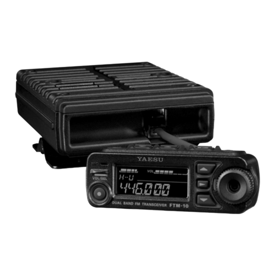
VHF/UFH FM TRANSCEIVER
FTM-10R/E
Technical Supplement
©2011 VERTEX STANDARD CO., LTD.
Introduction
This manual provides technical information necessary for
servicing the FTM-10R/E VHF/UHF FM Transceiver.
Servicing this equipment requires expertise in handling
surface-mount chip components. Attempts by non-
qualified persons to service this equipment may result
in permanent damage not covered by the warranty, and
may be illegal in some countries.
Two PCB layout diagrams are provided for each dou-
ble-sided circuit board in the Transceiver. Each side of
is referred to by the type of the majority of components
installed on that side ("leaded" or "chip-only"). In most cases one side has only chip components, and the
other has either a mixture of both chip and leaded components (trimmers, coils, electrolytic capacitors, ICs,
etc.), or leaded components only.
While we believe the technical information in this manual to be correct, VERTEX STANDARD assumes no
liability for damage that may occur as a result of typographical or other errors that may be present. Your
cooperation in pointing out any inconsistencies in the technical information would be appreciated.
The transceiver was assembled using Pb (lead) free solder, based on the RoHS specification.
Only lead-free solder (Alloy Composition: Sn-3.0Ag-0.5Cu) should be used for repairs performed on this appara-
tus. The solder stated above utilizes the alloy composition required for compliance with the lead-free specification,
and any solder with the above alloy composition may be used.
Specifications ........................................................................................................................................ 2
Exploded View & Miscellaneous Parts ............................................................................................ 3
Block Diagram ...................................................................................................................................... 5
Circuit Description .............................................................................................................................. 7
Alignment .............................................................................................................................................. 9
Board Unit (Schematics, Layouts & Parts)
MAIN-Unit ...................................................................................................................................... 17
PANEL-Unit .................................................................................................................................... 51
CH-SW-Unit .................................................................................................................................... 61
CONNECTOR-Unit ....................................................................................................................... 62
VERTEX STANDARD CO., LTD.
4-8-8 Nakameguro, Meguro-Ku, Tokyo 153-8644, Japan
VERTEX STANDARD U.S.A. Inc.
6125 Phyllis Drive, Cypress, California 90630, U.S.A.
YAESU UK LTD.
Unit 12, Sun Valley Business Park, Winnall Close
Winchester, Hampshire, SO23 0LB, U.K.
VERTEX STANDARD HK LTD.
Unit 1306-1308, 13F., Millennium City 2, 378 Kwun Tong Road,
Kwun Tong, Kowloon, Hong Kong
VERTEX STANDARD ( AUSTRALIA ) PTY., LTD.
Tally Ho Business Park, 10 Wesley Court, East Burwood, VIC, 3151
EH027M70E
Important Note
Contents
1
Advertisement
Table of Contents

Related Manuals for Verterx Standard Yaesu FTM-10R

Summary of Contents for Verterx Standard Yaesu FTM-10R
-
Page 1: Table Of Contents
VERTEX STANDARD CO., LTD. 4-8-8 Nakameguro, Meguro-Ku, Tokyo 153-8644, Japan VERTEX STANDARD U.S.A. Inc. VHF/UFH FM TRANSCEIVER 6125 Phyllis Drive, Cypress, California 90630, U.S.A. YAESU UK LTD. Unit 12, Sun Valley Business Park, Winnall Close FTM-10R/E Winchester, Hampshire, SO23 0LB, U.K. VERTEX STANDARD HK LTD. -
Page 2: Specifications
Specifications General Frequency Range: 0.5 - 1.8 MHz (AM BC) 76 - 108 MHz (FM BC) 108-137 MHz (Air Band) 137-174 MHz (144 MHz HAM) 174-222 MHz (GR1 VHF TV) 300-420 MHz (GR2 ) 420-470 MHz (430 MHz HAM) 470-800 MHz (GR1 UHF TV) 800-999 MHz (GR2 USA Cellular Blocked) 144.000 - 148.000 MHz or 144.000 - 146.000 MHz, 430.000 - 450.000 MHz or 430.000 - 440.000 MHz... -
Page 3: Exploded View & Miscellaneous Parts
Exploded View & Miscellaneous Parts RA1227200 SPACER (SP) FTM-10R/E Technical Supplement... - Page 4 Exploded View & Miscellaneous Parts Note FTM-10R/E Technical Supplement...
-
Page 5: Block Diagram
Block Diagram FTM-10R/E Technical Supplement... - Page 6 Block Diagram Note: FTM-10R/E Technical Supplement...
-
Page 7: Circuit Description
Circuit Description RECEPTION The detected audio passes through the de-emphasis net- VHF Reception work, a low-pass filter consisting of Q1419 (LM2902PWR) The incoming VHF signal is passed through the low-pass and associated circuitry, and then a high-pass filter con- filter network, antenna switching diodes and low-pass fil- sisting of Q1420 (LM2904PWR) and associated circuitry. - Page 8 Circuit Description stage power amplifier's gain is controlled by the APC cir- cuit. A portion of the output from the VCO Q1309 (2SC5006- The 40-Watts RF signal passes through the high-pass fil- T1), or Q1313 (2SC5006-T1) passes through the program- ter and low-pass filter networks, antenna switch D1014 m a b l e d i v i d e r s e c t i o n o f t h e P L L I C Q 1 3 0 4 (L709CER), another low-pass filter network, and then is...
-
Page 9: Alignment
Alignment RF Signal Generator with calibrated output level at 500 The FTM-10R/E has been carefully aligned at the fac- tory for the specified performance across the 144 MHz Deviation Meter (linear detector) and 430 MHz amateur bands. Realignment should there- ... - Page 10 Alignment PLL & Transmitter VCO VCV Adjustment Set up the test equipment as shown for transmitter align- Connect the DC voltmeter to TP1301. Referring to the ment. Maintain the supply voltage at 13.8V DC for all table below, tune the transceiver to each frequency listed. steps.
- Page 11 Alignment PLL Reference Frequency VHF Transmitter Output 1. Press the key repeatedly to display the fre- 1. Press the key repeatedly to display the fre- quency. quency. 2. Set the transceiver frequency to 440.050 MHz. 2. Set the transceiver frequency to 146.050 MHz. 3.
- Page 12 Alignment UHF Transmitter Output VHF Transmitter Deviation 1. Press the key repeatedly to display the fre- 1. Inject a 1 kHz audio tone at a level of 25 mV from the quency. AF generator into the microphone jack (pin 1). 2.
- Page 13 Alignment DCS TX Deviation CTCSS TX Deviation 1. Press the key repeatedly to display the fre- 1. Press the key repeatedly to display the fre- quency. quency. 2. Set the transceiver frequency to 146.050 MHz. 2. Set the transceiver frequency to 146.050 MHz. 3.
- Page 14 Alignment Center Meter Adjustment 26.Press the key to save the new setting. 1. Set the RF signal generator to 440.050 MHz. Set the 27.Press the key to save the new setting and generator for ±3.5 kHz deviation of a 1 kHz modula- exit the Alignment Menu mode.
- Page 15 Alignment UHF S-Meter Calibration Squelch Adjustment 1. Set the RF signal generator to 440.050 MHz. Set the 1. Set the RF signal generator to 146.050 MHz. Set the generator for ±3.5 kHz deviation of a 1 kHz modula- generator for ±3.5 kHz deviation of a 1 kHz modula- tion tone, and set the RF output level from the signal tion tone, and set the RF output level from the signal generator to -5 dBμ.
- Page 16 Alignment DC Voltmeter 1. Set the power supply voltage to 13.8 V. 2. Press the key repeatedly to display the Alignment Menu. 3. Press the key repeatedly to select Alignment Menu Item "A-9 BAT UP A-9 BAT UP A-9 BAT UP A-9 BAT UP...
-
Page 17: Main-Unit
MAIN-Unit (Lot. 1~4) Circuit Diagram 4.00 V 3.09 V 1.49 V 1.11 V <<+15.0 dBμ>> <<+12.9 dBμ>> 2.46 V <<-5.0 dBμ>> 8.45 V 8.91 V 0.74 V <<-1.0 dBμ>> 440 MHz : 2.06 V 0.48 V 2.46 V 8.91 V 8.45 V 0.96 V ((+1.7 dBμ)) ((+17.8 dBμ)) - Page 18 MAIN-Unit (Lot. 1~4) Parts Layout DTC144EE (26) 2SC4617 (BR) (Q1301, 1302, 1303, (Q1306, 1401, 1415, 1315, 1316, 1402, 1504, 1607, 1609, 1416, 1417, 1418, 1610, 1612, 1613, 1502, 1507, 1512, 1701, 1710, 1711, 1604, 1605, 1606, 1714) 1708, 1802, 1811, 2SC4915O (Q0) 1812, 1817) (Q1403, 1404, 1405,...
- Page 19 MAIN-Unit (Lot. 5~15) Circuit Diagram CAUTION Danger of explosion if battery is incorrectly replaced. Replace only with the same or equivalent type. FTM-10R/E Technical Supplement...
- Page 20 MAIN-Unit (Lot. 5~15) Parts Layout DTC144EE (26) 2SC4617 (BR) (Q1301, 1302, 1303, (Q1306, 1401, 1415, 1315, 1316, 1402, 1504, 1607, 1609, 1416, 1417, 1418, 1610, 1612, 1613, 1502, 1507, 1512, 1701, 1710, 1711, 1604, 1605, 1606, 1714) 1708, 1802, 1811, 2SC4915O (Q0) 1812, 1817, 1818) (Q1403, 1404, 1405,...
- Page 21 MAIN-Unit (Lot. 16~33) Circuit Diagram CAUTION Danger of explosion if battery is incorrectly replaced. Replace only with the same or equivalent type. FTM-10R/E Technical Supplement...
- Page 22 MAIN-Unit (Lot. 16~33) Parts Layout DTC144EE (26) 2SC4617 (BR) (Q1301, 1302, 1303, (Q1306, 1401, 1415, 1315, 1316, 1402, 1504, 1607, 1609, 1416, 1417, 1418, 1610, 1612, 1613, 1502, 1507, 1512, 1701, 1710, 1711, 1604, 1605, 1606, 1714) 1708, 1802, 1811, 2SC4915O (Q0) 1812, 1817, 1818) (Q1403, 1404, 1405,...
- Page 23 MAIN-Unit (Lot. 34~) Circuit Diagram CAUTION Danger of explosion if battery is incorrectly replaced. Replace only with the same or equivalent type. FTM-10R/E Technical Supplement...
- Page 24 MAIN-Unit (Lot. 34~) Parts Layout DTC144EE (26) 2SC4617 (BR) (Q1301, 1302, 1303, (Q1306, 1401, 1415, 1315, 1316, 1402, 1504, 1607, 1609, 1416, 1417, 1418, 1610, 1612, 1613, 1502, 1507, 1512, 1701, 1710, 1711, 1604, 1605, 1606, 1714) 1708, 1802, 1811, 2SC4915O (Q0) 1812, 1817, 1818) (Q1403, 1404, 1405,...
- Page 25 MAIN-Unit Parts List DESCRIPTION VALUE TOL. MFR'S DESIG VXSTD P/N VERS. LOT SIDE LAY ADR PCB with Components CS1936003 DST:USA, TYP:A2U CS1936004 DST:EXP, TYP:A1 CS1936005 DST:EXP, TYP:A2 CS1936006 DST:EXP, TYP:A3 CS1936007 DST:EU, TYP:B1 CS1936008 DST:EU, TYP:B2 CS1936009 DST:EXP, TYP:B3 CS1936010 DST:EU, TYP:C1 CS1936011 DST:EU, TYP:C2...
- Page 26 MAIN-Unit Parts List DESCRIPTION VALUE TOL. MFR'S DESIG VXSTD P/N VERS. LOT SIDE LAY ADR C 1055 CHIP CAP. 0.001uF GRM155B11H102KA01D K22178809 C 1056 CHIP CAP. 24pF GRM1552C1H240JZ01D K22178221 C 1056 CHIP CAP. 24pF GRM1552C1H240JZ01D K22178221 AUSTRALIA 2- C 1056 CHIP CAP.
- Page 27 MAIN-Unit Parts List DESCRIPTION VALUE TOL. MFR'S DESIG VXSTD P/N VERS. LOT SIDE LAY ADR C 1126 CHIP CAP. 22pF GRM1552C1H220JZ01D K22178220 C 1127 CHIP CAP. 22pF GRM1552C1H220JZ01D K22178220 C 1129 CHIP CAP. GRM1554C1H1R0BZ01D K22178287 C 1130 CHIP CAP. 10pF GRM1552C1H100BZ01D K22178297 C 1131...
- Page 28 MAIN-Unit Parts List DESCRIPTION VALUE TOL. MFR'S DESIG VXSTD P/N VERS. LOT SIDE LAY ADR C 1175 CHIP CAP. GRM1552C1H7R0BZ01D K22178294 C 1176 CHIP CAP. 0.1uF GRM155B11A104KA01D K22108802 C 1177 CHIP CAP. 0.001uF GRM155B11H102KA01D K22178809 C 1178 CHIP CAP. GRM1552C1H8R0BZ01D K22178295 C 1179 CHIP CAP.
- Page 29 MAIN-Unit Parts List DESCRIPTION VALUE TOL. MFR'S DESIG VXSTD P/N VERS. LOT SIDE LAY ADR C 1238 CHIP CAP. 100pF GRM1552C1H101JD01D K22178236 C 1240 CHIP CAP. 0.001uF GRM155B11H102KA01D K22178809 C 1241 CHIP CAP. 6.3V GRM155B30J105KE18D K22088803 C 1242 CHIP TA.CAP. 10uF TEESVA1A106M8R K78100028...
- Page 30 MAIN-Unit Parts List DESCRIPTION VALUE TOL. MFR'S DESIG VXSTD P/N VERS. LOT SIDE LAY ADR C 1362 CHIP CAP. 0.001uF GRM155B11H102KA01D K22178809 C 1363 CHIP CAP. 0.001uF GRM155B11H102KA01D K22178809 C 1364 CHIP CAP. 0.001uF GRM155B11H102KA01D K22178809 C 1365 CHIP CAP. 6.3V GRM155B30J105KE18D K22088803...
- Page 31 MAIN-Unit Parts List DESCRIPTION VALUE TOL. MFR'S DESIG VXSTD P/N VERS. LOT SIDE LAY ADR C 1446 CHIP CAP. 0.01uF GRM155B11E103KA01D K22148834 C 1447 CHIP CAP. 0.01uF GRM36B103K16PT K22128804 C 1447 CHIP CAP. 0.01uF GRM155B11E103KA01D K22148834 C 1448 CHIP CAP. 0.1uF GRM155B11A104KA01D K22108802...
- Page 32 MAIN-Unit Parts List DESCRIPTION VALUE TOL. MFR'S DESIG VXSTD P/N VERS. LOT SIDE LAY ADR C 1511 CHIP CAP. 6.3V GRM155B30J105KE18D K22088803 C 1512 CHIP CAP. 0.0047uF GRM36B472K25PT K22148830 C 1512 CHIP CAP. 0.0047uF GRM155B11H472KA01D K22178838 C 1513 CHIP CAP. 6.3V GRM155B30J105KE18D K22088803...
- Page 33 MAIN-Unit Parts List DESCRIPTION VALUE TOL. MFR'S DESIG VXSTD P/N VERS. LOT SIDE LAY ADR C 1574 CHIP CAP. 0.022uF GRM155B11C223KA01D K22128806 C 1575 CHIP CAP. 0.0047uF GRM36B472K25PT K22148830 C 1575 CHIP CAP. 0.0047uF GRM155B11H472KA01D K22178838 C 1576 CHIP CAP. 6.3V GRM155B30J105KE18D K22088803...
- Page 34 MAIN-Unit Parts List DESCRIPTION VALUE TOL. MFR'S DESIG VXSTD P/N VERS. LOT SIDE LAY ADR C 1713 CHIP CAP. 0.001uF GRM155B11H102KA01D K22178809 C 1714 CHIP CAP. GRM1552C1H7R0BZ01D K22178294 C 1716 CHIP CAP. 0.01uF GRM36B103K16PT K22128804 C 1716 CHIP CAP. 0.01uF GRM155B11E103KA01D K22148834 C 1717...
- Page 35 MAIN-Unit Parts List DESCRIPTION VALUE TOL. MFR'S DESIG VXSTD P/N VERS. LOT SIDE LAY ADR D 1032 DIODE HVC350B-TRF-E G2070596 D 1033 DIODE HVC350B-TRF-E G2070596 D 1035 DIODE HVC131TRF-E G2070676 D 1036 DIODE HVC131TRF-E G2070676 D 1037 DIODE MA2S72800L G2070858 D 1038 DIODE MA2S72800L...
- Page 36 MAIN-Unit Parts List DESCRIPTION VALUE TOL. MFR'S DESIG VXSTD P/N VERS. LOT SIDE LAY ADR FB1610 FERRITE BEADS BLM15AG121SN1D L1690843 FB1611 FERRITE BEADS BLM15AG121SN1D L1690843 FB1612 FERRITE BEADS BLM15AG121SN1D L1690843 FB1613 FERRITE BEADS BLM15AG121SN1D L1690843 FB1614 FERRITE BEADS BLM15AG121SN1D L1690843 FB1615 FERRITE BEADS BLM15AG121SN1D L1690843...
- Page 37 MAIN-Unit Parts List DESCRIPTION VALUE TOL. MFR'S DESIG VXSTD P/N VERS. LOT SIDE LAY ADR L 1040 M.RFC 0.068uH C1608CB-68NG-RF L1691042 AUSTRALIA 2- L 1040 M.RFC 0.068uH C1608CB-68NG-RF L1691042 EUROPE L 1040 M.RFC 0.068uH C1608CB-68NG-RF L1691042 EXPORT L 1040 M.RFC 0.068uH C1608CB-68NG-RF L1691042...
- Page 38 MAIN-Unit Parts List DESCRIPTION VALUE TOL. MFR'S DESIG VXSTD P/N VERS. LOT SIDE LAY ADR L 1310 COIL E2 0.3-1.1-3T-R L0022579 L 1311 M.RFC 0.0047uH TFL0816-4N7 L1690487 L 1312 M.RFC LK1608 1R0K-T L1690687 L 1313 M.RFC LK1608 1R0K-T L1690687 L 1314 M.RFC 0.39uH C1608CB-R39G-RF...
- Page 39 MAIN-Unit Parts List DESCRIPTION VALUE TOL. MFR'S DESIG VXSTD P/N VERS. LOT SIDE LAY ADR Q 1502 TRANSISTOR DTC144EE TL G3070075 Q 1503 LM2902PWR G1094009 Q 1504 TRANSISTOR 2SC4617 TL R G3346178R Q 1505 BU9253FS-E2 G1094359 Q 1506 CD4053BPWR G1093864 Q 1507 TRANSISTOR DTC144EE TL...
- Page 40 MAIN-Unit Parts List DESCRIPTION VALUE TOL. MFR'S DESIG VXSTD P/N VERS. LOT SIDE LAY ADR R 1015 CHIP RES. 1/16W RMC1/16 102JATP J24185102 R 1016 CHIP RES. 1/16W RMC1/16S 470JTH J24189009 R 1017 CHIP RES. 8.2k 1/16W RMC1/16S 822JTH J24189036 R 1018 CHIP RES.
- Page 41 MAIN-Unit Parts List DESCRIPTION VALUE TOL. MFR'S DESIG VXSTD P/N VERS. LOT SIDE LAY ADR R 1090 CHIP RES. 1/16W RMC1/16S 101JTH J24189013 R 1090 CHIP RES. 1/16W RMC1/16S 220JTH J24189005 W/ CE LABEL 5- R 1090 CHIP RES. 1/16W RMC1/16S 101JTH J24189013 W/O CE LABEL5-...
- Page 42 MAIN-Unit Parts List DESCRIPTION VALUE TOL. MFR'S DESIG VXSTD P/N VERS. LOT SIDE LAY ADR R 1165 CHIP RES. 1/16W RMC1/16S 561JTH J24189022 R 1166 CHIP RES. 1/16W RMC1/16S 561JTH J24189022 R 1167 CHIP RES. 1/16W RMC1/16S 101JTH J24189013 R 1168 CHIP RES.
- Page 43 MAIN-Unit Parts List DESCRIPTION VALUE TOL. MFR'S DESIG VXSTD P/N VERS. LOT SIDE LAY ADR R 1365 CHIP RES. 1/16W RMC1/16S 470JTH J24189009 R 1366 CHIP RES. 1/16W RMC1/16S 681JTH J24189023 R 1367 CHIP RES. 1/16W 0.5% RR0510R-153-D J24189147 R 1368 CHIP RES.
- Page 44 MAIN-Unit Parts List DESCRIPTION VALUE TOL. MFR'S DESIG VXSTD P/N VERS. LOT SIDE LAY ADR R 1450 CHIP RES. 1/16W RMC1/16S 101JTH J24189013 R 1451 CHIP RES. 1/16W RMC1/16S 102JTH J24189025 R 1452 CHIP RES. 1/16W RMC1/16S 102JTH J24189025 R 1456 CHIP RES.
- Page 45 MAIN-Unit Parts List DESCRIPTION VALUE TOL. MFR'S DESIG VXSTD P/N VERS. LOT SIDE LAY ADR R 1526 CHIP RES. 1/16W RMC1/16S 473JTH J24189045 R 1527 CHIP RES. 1/16W RMC1/16S 473JTH J24189045 R 1528 CHIP RES. 1/16W RMC1/16S 333JTH J24189043 R 1529 CHIP RES.
- Page 46 MAIN-Unit Parts List DESCRIPTION VALUE TOL. MFR'S DESIG VXSTD P/N VERS. LOT SIDE LAY ADR R 1607 CHIP RES. 1/16W RMC1/16S 560JTH J24189010 R 1608 CHIP RES. 1/16W RMC1/16S 560JTH J24189010 R 1609 CHIP RES. 1/16W RMC1/16S 560JTH J24189010 R 1610 CHIP RES.
- Page 47 MAIN-Unit Parts List DESCRIPTION VALUE TOL. MFR'S DESIG VXSTD P/N VERS. LOT SIDE LAY ADR R 1708 CHIP RES. 1/16W RMC1/16S 473JTH J24189045 R 1709 CHIP RES. 100k 1/16W RMC1/16S 104JTH J24189049 R 1710 CHIP RES. 1/16W RMC1/16S 683JTH J24189047 R 1711 CHIP RES.
- Page 48 MAIN-Unit Parts List DESCRIPTION VALUE TOL. MFR'S DESIG VXSTD P/N VERS. LOT SIDE LAY ADR R 1811 CHIP RES. 1/16W RMC1/16S 102JTH J24189025 R 1812 CHIP RES. 1/16W RMC1/16S 102JTH J24189025 R 1813 CHIP RES. 1/16W RMC1/16S 102JTH J24189025 R 1814 CHIP RES.
- Page 49 MAIN-Unit Parts List DESCRIPTION VALUE TOL. MFR'S DESIG VXSTD P/N VERS. LOT SIDE LAY ADR TH1304 THERMISTOR TBPS1R104K475H5Q G9090069 TH1801 THERMISTOR TBPS1R103K440H5Q G9090067 X 1301 XTAL NX5032SA 11.7MHz 11.7MHZ H0103320 X 1701 XTAL VT-200 32.768KHZ 20PPM/6PF H0103267 X 1702 XTL XJNGGIDANF 4MHz 4.000000MHz H0103314...
- Page 50 MAIN-Unit Parts List Note: FTM-10R/E Technical Supplement...
-
Page 51: Panel-Unit
PANEL-Unit (Lot. 1~15) Circuit Diagram Glows Green, Red : 3.00 V Glows White, Blue : 8.50 V DIMMER 1 DIMMER 5 Glows White : 6.60 V Glows Red : 1.15 V 3.96 V 8.62 V Glows White : 5.00 V 3.30 V 7.81 V Glows Green : 0.26 V... - Page 52 PANEL-Unit (Lot. 1~15) Parts Layout Side A CL-165HR/YG HZM27WA (27A) (D2013) (D2019) SPMA10-1104Q7NC 2SK1588 (Q) (D2004, 2005, 2006, (Q2011) 2007, 2008) Side B 2SC4617 (BR) DTC144EE (26) (Q2003, 2004, 2005, (Q2013, 2016, 2017, 2009) 2018) HD64F38124WV LC75822W LM2904PWR HL500-W01 TC7W53FU TA75S01F (SA) NJM78L05UA (8C) FMMTL718TA (L78)
- Page 53 PANEL-Unit (Lot. 16~) Circuit Diagram Glows Green, Red : 3.00 V Glows White, Blue : 8.50 V Glows White : 6.60 V DIMMER 1 DIMMER 5 Glows Red : 1.15 V 3.96 V 8.62 V Glows White : 5.00 V 3.30 V 7.81 V Glows Green : 0.26 V...
- Page 54 PANEL-Unit (Lot. 16~) Parts Layout Side A CL-165HR/YG HZM27WA (27A) (D2013) (D2019) SPMA10-1104Q7NC 2SK1588 (Q) (D2004, 2005, 2006, (Q2011) 2007, 2008) Side B 2SC4617 (BR) DTC144EE (26) (Q2003, 2004, 2005, (Q2013, 2016, 2017, 2009) 2018) HD64F38124WV LC75822W LM2904PWR HL500-W01 TC7W53FU TA75S01F (SA) NJM78L05UA (8C) FMMTL718TA (L78)
- Page 55 PANEL-Unit Parts List DESCRIPTION VALUE TOL. MFR'S DESIG VXSTD P/N VERS. LOT SIDE LAY ADR PCB with Components CS1937002 DST:USA CS1937003 DST:EXP CS1937004 DST:EU CS1937005 DST:AUS C 2001 CHIP CAP. 0.001uF GRM155B11H102KA01D K22178809 C 2002 CHIP CAP. 0.33uF 6.3V GRM155B10J334KE01D K22088801 C 2003 CHIP CAP.
- Page 56 PANEL-Unit Parts List DESCRIPTION VALUE TOL. MFR'S DESIG VXSTD P/N VERS. LOT SIDE LAY ADR C 2061 CHIP TA.CAP. 4.7uF TEESVA1C475M8R K78120031 C 2062 CHIP CAP. 0.001uF GRM155B11H102KA01D K22178809 C 2063 CHIP CAP. 0.001uF GRM155B11H102KA01D K22178809 C 2064 CHIP CAP. 6.3V GRM155B30J105KE18D K22088803...
- Page 57 PANEL-Unit Parts List DESCRIPTION VALUE TOL. MFR'S DESIG VXSTD P/N VERS. LOT SIDE LAY ADR Q 2009 TRANSISTOR 2SC4617 TL R G3346178R Q 2010 TRANSISTOR 2SA1774 TL R G3117748R Q 2011 2SK1588-T1-AZ G3815888 Q 2013 TRANSISTOR DTC144EE TL G3070075 Q 2014 NJM78L05UA-TE1 G1091325 Q 2015...
- Page 58 PANEL-Unit Parts List DESCRIPTION VALUE TOL. MFR'S DESIG VXSTD P/N VERS. LOT SIDE LAY ADR R 2060 CHIP RES. 4.7k 1/16W RMC1/16S 472JTH J24189033 R 2062 CHIP RES. 1/16W RMC1/16S 223JTH J24189041 R 2063 CHIP RES. 1/16W RMC1/16S 102JTH J24189025 R 2065 CHIP RES.
- Page 59 PANEL-Unit Parts List DESCRIPTION VALUE TOL. MFR'S DESIG VXSTD P/N VERS. LOT SIDE LAY ADR INTER CONNECTOR RA0884300 LCD HOLDER RA0884400 REFLECTOR SHEET RA0884900 DIFFUSER SHEET RA0885000 MIC HOLDER RUBBER RA0884200 TERMINAL PLATE RA0884600 FTM-10R/E Technical Supplement...
- Page 60 PANEL-Unit Note FTM-10R/E Technical Supplement...
-
Page 61: Ch-Sw-Unit
CH-SW-Unit Circuit Diagram Parts Layout Side A Side B Parts List REF. DESCRIPTION VALUE TOL. MFR’S DESIG VXSTD P/N VERS. LOT. SIDE LAY ADR. J 3001 CONNECTOR BM03B-SRSS-TBT(LF)(SN) P0091301 S 3001 ROTARY ENCODER TP70N97E20 13.5FT RY-8200 Q9000865... -
Page 62: Connector-Unit
CONNECTOR-Unit (Lot. 1~15) Circuit Diagram Parts Layout Side A Side B... - Page 63 CONNECTOR-Unit (Lot. 16~) Circuit Diagram Parts Layout Side A Side B Parts List REF. DESCRIPTION VALUE TOL. MFR’S DESIG VXSTD P/N VERS. LOT. SIDE LAY ADR. PCB with Components CB4022001 J 4001 CONNECTOR 06FLT-SM2-TB(LF)(SN) P1091255 J 4001 CONNECTOR 08FLT-SM2-TB(LF)(SN) P1091201 J 4002 CONNECTOR 448MRW-7P P0091487...
- Page 64 Copyright 2011 VERTEX STANDARD CO., LTD. All rights reserved No portion of this manual may be reproduced without the permission of VERTEX STANDARD CO., LTD.
Need help?
Do you have a question about the Yaesu FTM-10R and is the answer not in the manual?
Questions and answers