Table of Contents
Advertisement
Quick Links
Advertisement
Table of Contents

Related Manuals for Fibocom L850-GL


Summary of Contents for Fibocom L850-GL
- Page 1 L850-GL Hardware User Manual Version:1.0.6 Update date:Feb 26th, 2018...
- Page 2 2. Modify description of power consumption condition V1.0.5 2018-1-16 3. Optimize power on/off/reset timing 1. Modify COEX pin define V1.0.6 2018-2-26 2. Del L850-GL-02 product model Reproduction forbidden without Fibocom Wireless Inc. written authorization - All Rights Reserved. L850-GL Hardware User Manual Page 2 of 54...
-
Page 3: L850-Gl
Applicability Table Product model Description L850-GL-00 L850-GL-01 L850-GL-03 L850-GL-05 L850-GL-10 Reproduction forbidden without Fibocom Wireless Inc. written authorization - All Rights Reserved. L850-GL Hardware User Manual Page 3 of 54... -
Page 4: Table Of Contents
PCIe & USB ........................30 3.4.1 PCIe Interface ......................30 3.4.1.1 PCIe Interface Definition ..................30 3.4.1.2 PCIe Interface Application ................... 31 Reproduction forbidden without Fibocom Wireless Inc. written authorization - All Rights Reserved. L850-GL Hardware User Manual Page 4 of 54... - Page 5 Antenna Design ......................... 48 Structure Specification ........................50 Product Appearance ......................50 Dimension of Structure ....................... 50 M.2 Interface Model ......................51 Reproduction forbidden without Fibocom Wireless Inc. written authorization - All Rights Reserved. L850-GL Hardware User Manual Page 5 of 54...
- Page 6 Storage ..........................52 5.5.1 Storage Life ........................ 52 Packing ..........................52 5.6.1 Tray Package ......................52 5.6.2 Tray size ........................53 Reproduction forbidden without Fibocom Wireless Inc. written authorization - All Rights Reserved. L850-GL Hardware User Manual Page 6 of 54...
-
Page 7: Foreword
The document describes the electrical characteristics, RF performance, dimensions and application environment, etc. of L850-GL (hereinafter referred to as L850). With the assistance of the document and other instructions, the developers can quickly understand the hardware functions of L850 modules and develop products. -
Page 8: Overview
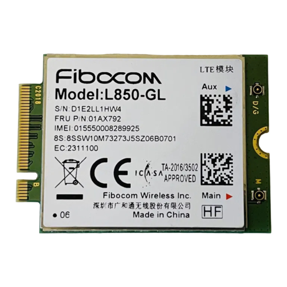
Weight: About 5.8 g Interface WWAN Main Antenna x 1 Antenna Connector WWAN Diversity Antenna x 1 Function Interface USIM 3V/1.8V Reproduction forbidden without Fibocom Wireless Inc. written authorization - All Rights Reserved. L850-GL Hardware User Manual Page 8 of 54... -
Page 9: Warning
(1) This device may not cause harmful interference, and (2) this device must accept any interference received, including interference that may cause undesired operation. Reproduction forbidden without Fibocom Wireless Inc. written authorization - All Rights Reserved. L850-GL Hardware User Manual... - Page 10 As long as 2 conditions above are met, further transmitter test will not be required. However, the OEM integrator is still responsible for testing their end-product for any additional compliance requirements required with this module installed. Reproduction forbidden without Fibocom Wireless Inc. written authorization - All Rights Reserved. L850-GL Hardware User Manual Page 10 of 54...
-
Page 11: Ic Statement
Cet appareil est conforme à la norme RSS-310 d'Industrie Canada. L'opération est soumise à la condition que cet appareil ne provoque aucune interférence nuisible. Reproduction forbidden without Fibocom Wireless Inc. written authorization - All Rights Reserved. L850-GL Hardware User Manual... -
Page 12: Ce Statement
2.3.3 CE Statement ► EU Regulatory Conformance Hereby, We, Fibocom Wireless Inc. declares that the radio equipment type L850-GL is in compliance with the Directive 2014/53/EU. In all cases assessment of the final product must be mass against the Essential requirements of the Directive 2014/53/EU Articles 3.1(a) and (b), safety and EMC respectively, as well as any relevant... -
Page 13: Ca Combinations
3+3+1, 3+3+5, 3+3+7, 3+3+20, 3+3+28 2 intra-band(contiguous) 2+66+66, 5+66+66, 13+66+66 plus inter-band 7+7+3, 7+7+28 Intra-band(non-contiguous) 41, 66 Intra-band(contiguous) 40, 41, 66 Reproduction forbidden without Fibocom Wireless Inc. written authorization - All Rights Reserved. L850-GL Hardware User Manual Page 13 of 54... -
Page 14: Application Framework
RF contains the followings: RF Transceiver RF Power/PA RF Front end RF Filter Antenna Connector Reproduction forbidden without Fibocom Wireless Inc. written authorization - All Rights Reserved. L850-GL Hardware User Manual Page 14 of 54... -
Page 15: Reproduction Forbidden Without Fibocom Wireless Inc. Written Authorization - All Rights Reserved
Figure 2-2 Hardware Block Diagram Reproduction forbidden without Fibocom Wireless Inc. written authorization - All Rights Reserved. L850-GL Hardware User Manual Page 15 of 54... -
Page 16: Application Interface
The L850 module applies standard M.2 Key-B interface, with a total of 75 pins. 3.1.1 Pin Map Figure 3-1 Pin Map Note: Reproduction forbidden without Fibocom Wireless Inc. written authorization - All Rights Reserved. L850-GL Hardware User Manual Page 16 of 54... -
Page 17: Pin Definition
I2S Serial clock, I2S_CLK CMOS 1.8V Reserved GND, L850 M.2 module is configured as CONFIG_0 the WWAN – PCIe, USB3.0 interface type Reproduction forbidden without Fibocom Wireless Inc. written authorization - All Rights Reserved. L850-GL Hardware User Manual Page 17 of 54... -
Page 18: Reproduction Forbidden Without Fibocom Wireless Inc. Written Authorization - All Rights Reserved
I2C Serial data input/output, GNSS_SDA CMOS 1.8V Reserved PETp0 PCIe TX Differential signals Positive GNSS Interrupt Request, GNSS_IRQ CMOS 1.8V Reserved Power Supply Reproduction forbidden without Fibocom Wireless Inc. written authorization - All Rights Reserved. L850-GL Hardware User Manual Page 18 of 54... -
Page 19: Reproduction Forbidden Without Fibocom Wireless Inc. Written Authorization - All Rights Reserved
3.3/1.8V ANTCTL0 Tunable ANT CTRL0 CMOS 1.8V Wireless Coexistence between WWAN COEX3 CMOS 1.8V and WiFi/BT modules, based on BT-SIG Reproduction forbidden without Fibocom Wireless Inc. written authorization - All Rights Reserved. L850-GL Hardware User Manual Page 19 of 54... -
Page 20: Reproduction Forbidden Without Fibocom Wireless Inc. Written Authorization - All Rights Reserved
Reset Value: The initial status after module reset, not the status when working. H: High Voltage Level Low Voltage Level PD: Pull-Down Reproduction forbidden without Fibocom Wireless Inc. written authorization - All Rights Reserved. L850-GL Hardware User Manual Page 20 of 54... -
Page 21: Power Supply
The L850 module should be powered through the +3.3V pins, and the power supply design is shown in Figure 3-2: Figure 3-2 Power Supply Design Reproduction forbidden without Fibocom Wireless Inc. written authorization - All Rights Reserved. L850-GL Hardware User Manual Page 21 of 54... -
Page 22: Logic Level
Figure 3-3 Power Supply Limit 3.2.2 Logic level The L850module 1.8V logic level definition as shown in the following table: Reproduction forbidden without Fibocom Wireless Inc. written authorization - All Rights Reserved. L850-GL Hardware User Manual Page 22 of 54... -
Page 23: Power Consumption
LTE FDD Data call Band 1 @+23dBm LTE FDD Data call Band 2 @+23dBm LTE FDD LTE-RMS LTE FDD Data call Band 3 @+23dBm Reproduction forbidden without Fibocom Wireless Inc. written authorization - All Rights Reserved. L850-GL Hardware User Manual Page 23 of 54... -
Page 24: Reproduction Forbidden Without Fibocom Wireless Inc. Written Authorization - All Rights Reserved
1+3+7, 1+3+8,1+3+19, 1+3+20, 1+3+28, Band 2 @+22dBm 1+7+20, 1+7+28, 1+8+11, 1+19+21 2+4+5, 2+4+13, 2+5+30, 2+12+30, 2+29+30 Band 3 @+22dBm 1170 Reproduction forbidden without Fibocom Wireless Inc. written authorization - All Rights Reserved. L850-GL Hardware User Manual Page 24 of 54... -
Page 25: Control Signal
Asserted to reset module PCIe CMOS PERST# interface default. If module went into 3.3V core dump, it will reset whole Reproduction forbidden without Fibocom Wireless Inc. written authorization - All Rights Reserved. L850-GL Hardware User Manual Page 25 of 54... -
Page 26: Module Start-Up
The start-up timing is shown in Figure 3-5: +3.3V FULL_CARD_POWER_OFF# RESET# PERST# typical 10s Module State Initialization Activation(AT Command Ready) Figure 3-5 Timing Control for Start-up Reproduction forbidden without Fibocom Wireless Inc. written authorization - All Rights Reserved. L850-GL Hardware User Manual Page 26 of 54... -
Page 27: Module Shutdown
RESET# should asserted before FULL_CARD_POWER_OFF# 10ms 30ms off1 30ms PERST# should asserted after RESET# off2 off1 Reproduction forbidden without Fibocom Wireless Inc. written authorization - All Rights Reserved. L850-GL Hardware User Manual Page 27 of 54... -
Page 28: Module Reset
+3.3V FULL_CARD_POWER_OFF# RESET# res1 res2 PERST# typical 10s Module State Restart Activation PMU RESET Activation Figure 3-8 Reset control timing1 Reproduction forbidden without Fibocom Wireless Inc. written authorization - All Rights Reserved. L850-GL Hardware User Manual Page 28 of 54... -
Page 29: Pcie Reset
Module supports PCIe goes in to D3cold L2 state in Win10 system. The D0->D3cold L2@S0/S0ix/S3 ->D0 timing is shown in figure 3-10: Figure 3-10 PCIe reset timing Reproduction forbidden without Fibocom Wireless Inc. written authorization - All Rights Reserved. L850-GL Hardware User Manual Page 29 of 54... -
Page 30: Pcie & Usb
If module went into coredump, it will PERST# CMOS 3.3V reset whole module, not only PCIe interface. Active low, internal pull up(10KΩ) Reproduction forbidden without Fibocom Wireless Inc. written authorization - All Rights Reserved. L850-GL Hardware User Manual Page 30 of 54... -
Page 31: Pcie Interface Application
The impedance of differential signal pair lines is recommended to be 100 ohm, and can be controlled to 80~120 ohm in accordance with PCIe protocol; Reproduction forbidden without Fibocom Wireless Inc. written authorization - All Rights Reserved. L850-GL Hardware User Manual Page 31 of 54... -
Page 32: Reproduction Forbidden Without Fibocom Wireless Inc. Written Authorization - All Rights Reserved
The length match should be close to the signal pin and pass the small-angle bending design. Reproduction forbidden without Fibocom Wireless Inc. written authorization - All Rights Reserved. L850-GL Hardware User Manual Page 32 of 54... -
Page 33: Usb Interface
USB3.0 receive data minus USB3.0_RX+ USB3.0 receive data plus 3.4.2.2 USB2.0 Interface Application The reference circuit is shown in Figure 3-14: Reproduction forbidden without Fibocom Wireless Inc. written authorization - All Rights Reserved. L850-GL Hardware User Manual Page 33 of 54... -
Page 34: Usb3.0 Interface Application
The two pairs differential signal lines should be parallel and have the equal length, the right Reproduction forbidden without Fibocom Wireless Inc. written authorization - All Rights Reserved. L850-GL Hardware User Manual Page 34 of 54... -
Page 35: Usim Interface
3.5.2.1 N.C. SIM Card Slot The reference circuit design for N.C. (Normally Closed) SIM card slot is shown in Figure 3-16: Reproduction forbidden without Fibocom Wireless Inc. written authorization - All Rights Reserved. L850-GL Hardware User Manual Page 35 of 54... -
Page 36: Sim Card Slot
When the SIM card is inserted, it connects the short circuit between CD and SW pins, and drives the SIM_DETECT pin high. Reproduction forbidden without Fibocom Wireless Inc. written authorization - All Rights Reserved. L850-GL Hardware User Manual Page 36 of 54... -
Page 37: Usim Hot-Plugging
The UIM_CLK and UIM_DATA signal lines should be isolated by GND to avoid crosstalk Reproduction forbidden without Fibocom Wireless Inc. written authorization - All Rights Reserved. L850-GL Hardware User Manual Page 37 of 54... -
Page 38: Status Indicator
Figure 3-18 LED Driving Circuit Note: The resistance of LED current-limiting resistor is selected according to the driving voltage and the driving current. Reproduction forbidden without Fibocom Wireless Inc. written authorization - All Rights Reserved. L850-GL Hardware User Manual Page 38 of 54... -
Page 39: Interrupt Control
High/Floating The module keeps the default emission power Lower the maximum emission power to the threshold value of the module. Reproduction forbidden without Fibocom Wireless Inc. written authorization - All Rights Reserved. L850-GL Hardware User Manual Page 39 of 54... -
Page 40: Clock Interface
The L850 module provides four config pins for the configuration as the WWAN-PCIe, USB3.0 type M.2 module: Pin Name Reset Value Pin Description Type CONFIG_3 CONFIG_0 Internally connected to GND Reproduction forbidden without Fibocom Wireless Inc. written authorization - All Rights Reserved. L850-GL Hardware User Manual Page 40 of 54... -
Page 41: Other Interfaces
Please refer to PCI Express M.2 Specification Rev1.1” for more details. 3.11 Other Interfaces The module does not support other interfaces yet. Reproduction forbidden without Fibocom Wireless Inc. written authorization - All Rights Reserved. L850-GL Hardware User Manual Page 41 of 54... -
Page 42: Radio Frequency
The L850 module adopts standard M.2 module RF connectors, the model name is 818004607 from ECT company, and the connector size is 2*2*0.6m. The connector dimension is shown as following picture: Reproduction forbidden without Fibocom Wireless Inc. written authorization - All Rights Reserved. L850-GL Hardware User Manual Page 42 of 54... -
Page 43: Reproduction Forbidden Without Fibocom Wireless Inc. Written Authorization - All Rights Reserved
Figure 4-2 RF connector dimensions Figure 4-3 0.81mm coaxial antenna dimensions Figure 4-4 Schematic diagram of 0.81mm coaxial antenna connected to the RF connector Reproduction forbidden without Fibocom Wireless Inc. written authorization - All Rights Reserved. L850-GL Hardware User Manual Page 43 of 54... -
Page 44: Operating Band
2300MHz LTE TDD 2300 - 2400 Band 41 2500MHZ LTE TDD 2496 - 2690 GPS L1 1575.42±1.023 GLONASS L1 1602.5625±4 Reproduction forbidden without Fibocom Wireless Inc. written authorization - All Rights Reserved. L850-GL Hardware User Manual Page 44 of 54... -
Page 45: Transmitting Power
10MHz Bandwidth, 1 RB 23±2.7 Band 28 23+2.7/-3.2 23±1 10MHz Bandwidth, 1 RB Band 30 22±1 10MHz Bandwidth, 1 RB 23±2.7 Reproduction forbidden without Fibocom Wireless Inc. written authorization - All Rights Reserved. L850-GL Hardware User Manual Page 45 of 54... -
Page 46: Receiver Sensitivity
10MHz Bandwidth Band 17 -93.3 -102.5 10MHz Bandwidth Band 18 -96.3 -103 10MHz Bandwidth Band 19 -96.3 -103 10MHz Bandwidth Reproduction forbidden without Fibocom Wireless Inc. written authorization - All Rights Reserved. L850-GL Hardware User Manual Page 46 of 54... -
Page 47: Gnss
BeiDou tracking 120mA / -130dbm GPS Sleep 0.7mA GLONASS Sleep 0.8mA BeiDou Sleep 0.7mA TTFF Cold start 37s / -130dBm Reproduction forbidden without Fibocom Wireless Inc. written authorization - All Rights Reserved. L850-GL Hardware User Manual Page 47 of 54... -
Page 48: Antenna Design
WCDMA band 4(1700) : 445 MHz WCDMA band 5(850) : 70 MHz WCDMA band 8(900) : 80 MHz Bandwidth(LTE) LTE band 1(2100): 250 MHz Reproduction forbidden without Fibocom Wireless Inc. written authorization - All Rights Reserved. L850-GL Hardware User Manual Page 48 of 54... -
Page 49: Reproduction Forbidden Without Fibocom Wireless Inc. Written Authorization - All Rights Reserved
BeiDou: 4 MHz Impedance 50Ohm Input power > 26dBm average power WCDMA & LTE Recommended standing-wave ≤ 2: 1 ratio (SWR) Reproduction forbidden without Fibocom Wireless Inc. written authorization - All Rights Reserved. L850-GL Hardware User Manual Page 49 of 54... -
Page 50: Structure Specification
5.2 Dimension of Structure The structural dimension of the L850 module is shown in Figure 5-2: Figure 5-2 Dimension of Structure Reproduction forbidden without Fibocom Wireless Inc. written authorization - All Rights Reserved. L850-GL Hardware User Manual Page 50 of 54... -
Page 51: Interface Model
LOTES company with the model APCI0026-P001A as shown in Figure 5-3. The package of connector, please refer to the specification. Reproduction forbidden without Fibocom Wireless Inc. written authorization - All Rights Reserved. L850-GL Hardware User Manual Page 51 of 54... -
Page 52: Storage
5.6.1 Tray Package The L850 module uses tray package, 20 pcs are packed in each tray, with 5 trays in each box and 6 boxes Reproduction forbidden without Fibocom Wireless Inc. written authorization - All Rights Reserved. L850-GL Hardware User Manual... -
Page 53: Tray Size
Tray packaging process is shown in Figure 5-4: Figure 5-4 Tray Packaging Process 5.6.2 Tray size The pallet size is 330*175*6.0mm, as shown in Figure 5-5: Reproduction forbidden without Fibocom Wireless Inc. written authorization - All Rights Reserved. L850-GL Hardware User Manual Page 53 of 54... - Page 54 Figure 5-5Tray Size (Unit: mm) ITEM DIM(Unit: mm) 330.0±0.5 175.0±0.5 6.0±0.3 0.5±0.1 43±0.3 33.0±0.3 294.0±0.3 159.0±0.3 20.0±0.5 9.0±0.5 24.5±0.5 187.5±0.2 105.0±0.2 9.0±0.2 Reproduction forbidden without Fibocom Wireless Inc. written authorization - All Rights Reserved. L850-GL Hardware User Manual Page 54 of 54...
Need help?
Do you have a question about the L850-GL and is the answer not in the manual?
Questions and answers