Fibocom L850-GL Series Hardware Manual
Hide thumbs
Also See for L850-GL Series:
- Hardware user manual (51 pages) ,
- Hardware user manual (54 pages)
Table of Contents
Advertisement
Advertisement
Table of Contents

Related Manuals for Fibocom L850-GL Series


Summary of Contents for Fibocom L850-GL Series
- Page 1 FIBOCOM L850-GL Series Hardware Guide Version: V1.1.5 Date: 2020-06-20...
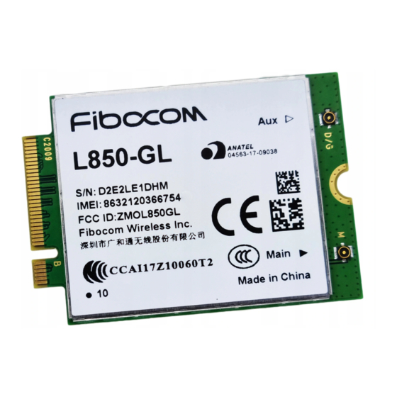
- Page 2 Applicability Type Product Model Description L850-GL-00 L850-GL-01 L850-GL-02 L850-GL-03 L850-GL-05 L850-GL-10 L850-GL-10 series (except L850-GL-10-06) L850-GL-10-06 L850-GL-12 L850-GL-20 Reproduction forbidden without Fibocom Wireless Inc. written authorization - All Rights Reserved. FIBOCOM L850-GL Series Hardware Guide Page 2 of 59...
- Page 3 Trademark The trademark is registered and owned by Fibocom Wireless Inc. Reproduction forbidden without Fibocom Wireless Inc. written authorization - All Rights Reserved. FIBOCOM L850-GL Series Hardware Guide Page 3 of 59...
- Page 4 ● Add antenna of B30 requirement, update power consumption and RX sensitivity ● Modify COEX pin define V1.0.6 Lei Daijun 2018-02-26 ● Delete L850-GL-02 product model Reproduction forbidden without Fibocom Wireless Inc. written authorization - All Rights Reserved. FIBOCOM L850-GL Series Hardware Guide Page 4 of 59...
- Page 5 V1.0.1 Lei Daijun 2016-12-16 ● Update the Pin Definition: change pin65 to NC V1.0.0 Lei Daijun 2016-12-08 Initial version Reproduction forbidden without Fibocom Wireless Inc. written authorization - All Rights Reserved. FIBOCOM L850-GL Series Hardware Guide Page 5 of 59...
-
Page 6: Table Of Contents
PCIe Interface ......................33 3.4.1.1 PCIe Interface Definition ......................33 3.4.1.2 PCIe Interface Application ......................34 3.4.2 USB Interface ......................35 Reproduction forbidden without Fibocom Wireless Inc. written authorization - All Rights Reserved. FIBOCOM L850-GL Series Hardware Guide Page 6 of 59... - Page 7 Structure Specification ....................54 Product Appearance ..................... 54 Dimension of Structure ....................54 M.2 Interface Model ...................... 55 M.2 Connector ......................55 Reproduction forbidden without Fibocom Wireless Inc. written authorization - All Rights Reserved. FIBOCOM L850-GL Series Hardware Guide Page 7 of 59...
- Page 8 Storage ......................... 56 5.5.1 Storage Life ......................... 56 Packing ......................... 56 5.6.1 Tray Package ....................... 56 5.6.2 Tray Size ........................59 Reproduction forbidden without Fibocom Wireless Inc. written authorization - All Rights Reserved. FIBOCOM L850-GL Series Hardware Guide Page 8 of 59...
-
Page 9: Foreword
(DTE - DCE) interface for Short Message Service (SMS) and Cell Broadcast Service (CBS) PCI Express M.2 Specification Rev1.2 1.3 Related Documents FIBOCOM Design Guide_RF Antenna Reproduction forbidden without Fibocom Wireless Inc. written authorization - All Rights Reserved. FIBOCOM L850-GL Series Hardware Guide Page 9 of 59... -
Page 10: Overview
Extended operating temperature: -20°C~+65°C Temperature Storage temperature: -40°C~+85°C Interface: M.2 Key-B Physical Dimension : 30×42×2.3mm characteristics Weight: About 6.2 g Reproduction forbidden without Fibocom Wireless Inc. written authorization - All Rights Reserved. FIBOCOM L850-GL Series Hardware Guide Page 10 of 59... - Page 11 3GPP specifications. For normal operating temperature, LTE FDD Band 4 and 13 can support temperature ranging from -20°C to +60°C. Reproduction forbidden without Fibocom Wireless Inc. written authorization - All Rights Reserved. FIBOCOM L850-GL Series Hardware Guide...
-
Page 12: Ca Combinations
2 intra-band (contiguous) 2+66+66, 5+66+66, 13+66+66 plus inter-band 7+7+3, 7+7+28 Intra-band (non-contiguous) 41, 66 40, 41, 66 Intra-band (contiguous) Reproduction forbidden without Fibocom Wireless Inc. written authorization - All Rights Reserved. FIBOCOM L850-GL Series Hardware Guide Page 12 of 59... -
Page 13: Application Framework
Main ANT Module Power Supply ON/OFF# RESET# PCIe USB2.0 USB3.1 EINT Indicator Host application Control Card Figure2-1 Application framework Reproduction forbidden without Fibocom Wireless Inc. written authorization - All Rights Reserved. FIBOCOM L850-GL Series Hardware Guide Page 13 of 59... -
Page 14: Hardware Block Diagram
LB FEM Transceiver 1st Div ANT CLOCK Div RX MB FEM GNSS/ Tunable ANT Beidou Figure 2-2 Hardware block diagram Reproduction forbidden without Fibocom Wireless Inc. written authorization - All Rights Reserved. FIBOCOM L850-GL Series Hardware Guide Page 14 of 59... -
Page 15: Application Interface
The L850 module applies standard M.2 Key-B interface, with a total of 75 pins. 3.1.1 Pin Map Figure 3-1 Pin map Note: Pin “Notch” represents the gap of the gold fingers. Reproduction forbidden without Fibocom Wireless Inc. written authorization - All Rights Reserved. FIBOCOM L850-GL Series Hardware Guide Page 15 of 59... -
Page 16: Pin Definition
GND, L850 M.2 module is configured as CONFIG_0 the WWAN – PCIe, USB3.1 interface type I2S serial receive data, I2S_RX 1.8V Reserved Reproduction forbidden without Fibocom Wireless Inc. written authorization - All Rights Reserved. FIBOCOM L850-GL Series Hardware Guide Page 16 of 59... - Page 17 I2C serial data input/output, GNSS_SDA 1.8V Reserved PCIe TX differential signal PETp0 Positive GNSS interrupt request output, GNSS_IRQ 1.8V Reserved Power Supply Reproduction forbidden without Fibocom Wireless Inc. written authorization - All Rights Reserved. FIBOCOM L850-GL Series Hardware Guide Page 17 of 59...
- Page 18 Positive MIPI interface tunable ANT, RFFE_SCLK 1.8V RFFE clock Power Supply MIPI interface tunable ANT, RFFE_SDATA 1.8V RFFE data Reproduction forbidden without Fibocom Wireless Inc. written authorization - All Rights Reserved. FIBOCOM L850-GL Series Hardware Guide Page 18 of 59...
- Page 19 Power input Power Supply GND, L850 M.2 module is configured as CONFIG_2 the WWAN – PCIe, USB3.1 interface type Reproduction forbidden without Fibocom Wireless Inc. written authorization - All Rights Reserved. FIBOCOM L850-GL Series Hardware Guide Page 19 of 59...
-
Page 20: Power Supply
The L850 module should be powered through the +3.3V pins, and the power supply design is shown in Figure 3-2: Reproduction forbidden without Fibocom Wireless Inc. written authorization - All Rights Reserved. FIBOCOM L850-GL Series Hardware Guide Page 20 of 59... - Page 21 1.5A, so the power source should be not lower than 3.135V, or the module may shut down or reboot. The power supply limits are shown in Figure 3-3: Reproduction forbidden without Fibocom Wireless Inc. written authorization - All Rights Reserved. FIBOCOM L850-GL Series Hardware Guide...
-
Page 22: Logic Level
Sleep LTE FDD Paging cycle #128 frames (1.28s DRx cycle) LTE TDD Paging cycle #128 frames (1.28s DRx cycle) Reproduction forbidden without Fibocom Wireless Inc. written authorization - All Rights Reserved. FIBOCOM L850-GL Series Hardware Guide Page 22 of 59... - Page 23 LTE FDD Data call Band 30 @+23dBm LTE FDD Data call Band 66 @+23dBm LTE TDD Data call Band 38 @+23dBm LTE TDD Reproduction forbidden without Fibocom Wireless Inc. written authorization - All Rights Reserved. FIBOCOM L850-GL Series Hardware Guide Page 23 of 59...
- Page 24 Band 41 @+22dBm Band 66 @+22dBm Note: The data above is an average value tested on some samples at 25°C temperature. Reproduction forbidden without Fibocom Wireless Inc. written authorization - All Rights Reserved. FIBOCOM L850-GL Series Hardware Guide Page 24 of 59...
-
Page 25: Control Signal
FCPO#. It also should reserve a 100K pull down resistor on AP side. The reference design is shown in Figure3-4: Reproduction forbidden without Fibocom Wireless Inc. written authorization - All Rights Reserved. FIBOCOM L850-GL Series Hardware Guide Page 25 of 59... -
Page 26: Start-Up Timing Sequence
When USB is used as data transfer interface, follow timing above in PERST# connecting with host, otherwise don’t control PERST# in PERST# floating condition. Reproduction forbidden without Fibocom Wireless Inc. written authorization - All Rights Reserved. FIBOCOM L850-GL Series Hardware Guide... -
Page 27: Module Shutdown
When USB is used as data transfer interface, follow timing above in PERST# connecting with host, otherwise don’t control PERST# in PERST# floating condition. Reproduction forbidden without Fibocom Wireless Inc. written authorization - All Rights Reserved. FIBOCOM L850-GL Series Hardware Guide... -
Page 28: Module Reset
+3.3V FCPO# RESET# off2 PERST# typical 10s Module State Activation Baseband reset Initialization Activation Figure 3-8 Reset timing 1 Reproduction forbidden without Fibocom Wireless Inc. written authorization - All Rights Reserved. FIBOCOM L850-GL Series Hardware Guide Page 28 of 59... -
Page 29: Pcie Link State
CLKREQ# de-asserted in D3 L2. We recommend keep CLKREQ# de- cold asserted in D3 cold Reproduction forbidden without Fibocom Wireless Inc. written authorization - All Rights Reserved. FIBOCOM L850-GL Series Hardware Guide Page 29 of 59... -
Page 30: D0 L1.2
The D0 L0@S0/S0ix→D3 L2@S0/S0ix→D0 L0@S0/S0ix timing cold is shown in Figure 3-11 and Figure 3-12: Reproduction forbidden without Fibocom Wireless Inc. written authorization - All Rights Reserved. FIBOCOM L850-GL Series Hardware Guide Page 30 of 59... - Page 31 When USB is used as data transfer interface in Chrome/Android/Linux OS, there is no PCIe link state, so don’t need to follow timing above. Reproduction forbidden without Fibocom Wireless Inc. written authorization - All Rights Reserved. FIBOCOM L850-GL Series Hardware Guide...
-
Page 32: Timing Application
It must disconnect PCIe port, only keep USB connecting. Chrome OS If keep PCIe and USB connecting both, it needs disable PCIe /Android/Linux by BIOS/UEFI of PC Reproduction forbidden without Fibocom Wireless Inc. written authorization - All Rights Reserved. FIBOCOM L850-GL Series Hardware Guide Page 32 of 59... -
Page 33: Pcie Interface
Active low, open drain output and should add external pull up (100KΩ) on platform Reproduction forbidden without Fibocom Wireless Inc. written authorization - All Rights Reserved. FIBOCOM L850-GL Series Hardware Guide Page 33 of 59... -
Page 34: Pcie Interface Application
20mil, and the line caused by bending should be greater than 1.5 times line width at least. When a serpentine line is used for length match with another line, the bended length of each segment Reproduction forbidden without Fibocom Wireless Inc. written authorization - All Rights Reserved. FIBOCOM L850-GL Series Hardware Guide... -
Page 35: Usb Interface
USB interface initialized with host driver, and then mapped NCM and ACM ports in Chrome/Linux/Android OS. The NCM ports are used for data transfer. The ACM port is used for AT command. The port can be Reproduction forbidden without Fibocom Wireless Inc. written authorization - All Rights Reserved. FIBOCOM L850-GL Series Hardware Guide... -
Page 36: Usb Interface Definition
GND vertically and horizontally. 3.4.2.3 USB3.0 Interface Application The reference circuit is shown in Figure 3-17: Reproduction forbidden without Fibocom Wireless Inc. written authorization - All Rights Reserved. FIBOCOM L850-GL Series Hardware Guide Page 36 of 59... -
Page 37: Usim Interface
Active high, and high level indicates 1.8V SIM card is inserted; and low level indicates SIM card is detached. Reproduction forbidden without Fibocom Wireless Inc. written authorization - All Rights Reserved. FIBOCOM L850-GL Series Hardware Guide Page 37 of 59... -
Page 38: Usim Interface Circuit
When the SIM card is detached, it connects an open circuit between CD and SW pins, and drives the SIM_DETECT pin low. Reproduction forbidden without Fibocom Wireless Inc. written authorization - All Rights Reserved. FIBOCOM L850-GL Series Hardware Guide Page 38 of 59... -
Page 39: Usim Hot-Plug
If it is difficult for the layout, the whole SIM signal lines should be wrapped with GND as a group at Reproduction forbidden without Fibocom Wireless Inc. written authorization - All Rights Reserved. FIBOCOM L850-GL Series Hardware Guide Page 39 of 59... -
Page 40: Status Indicator
Figure 3-20 LED driving circuit Note: The resistance of LED current-limiting resistor is selected according to the driving voltage and the driving current. Reproduction forbidden without Fibocom Wireless Inc. written authorization - All Rights Reserved. FIBOCOM L850-GL Series Hardware Guide Page 40 of 59... -
Page 41: Interrupt Control
Reset Value Pin Description Type 26M clock output used for external audio SYSCLK 1.8V codec and GNSS, etc., default disabled Reproduction forbidden without Fibocom Wireless Inc. written authorization - All Rights Reserved. FIBOCOM L850-GL Series Hardware Guide Page 41 of 59... -
Page 42: Ant Tunable Interface
Internally connected to GND CONFIG_2 Internally connected to GND The M.2 module configuration is shown in the following table: Reproduction forbidden without Fibocom Wireless Inc. written authorization - All Rights Reserved. FIBOCOM L850-GL Series Hardware Guide Page 42 of 59... - Page 43 (pin1) Host Interface Configuration WWAN–USB3.1 Gen1, PCIe Gen1 Please refer to “PCI Express M.2 Specification Rev1.2” for more details. Reproduction forbidden without Fibocom Wireless Inc. written authorization - All Rights Reserved. FIBOCOM L850-GL Series Hardware Guide Page 43 of 59...
-
Page 44: Radio Frequency
L850 module uses standard M.2 RF connectors. The RF connector part number is 818004607 manufactured by ECT Corporation, and the size is 2×2×0.6mm. The connector dimension is shown as following picture: Reproduction forbidden without Fibocom Wireless Inc. written authorization - All Rights Reserved. FIBOCOM L850-GL Series Hardware Guide Page 44 of 59... - Page 45 Figure 4-3 0.81mm coaxial antenna dimensions Figure 4-4 Schematic diagram of 0.81mm coaxial antenna connected to the RF connector Reproduction forbidden without Fibocom Wireless Inc. written authorization - All Rights Reserved. FIBOCOM L850-GL Series Hardware Guide Page 45 of 59...
-
Page 46: Rf Connector Assembly
JIG must be lifted up vertically to PCB surface (see Figure 4-7 and 4-8). Figure 4-6 Pulling JIG Figure 4-7 Lift up pulling JIG Reproduction forbidden without Fibocom Wireless Inc. written authorization - All Rights Reserved. FIBOCOM L850-GL Series Hardware Guide Page 46 of 59... - Page 47 Figure 4-8 Pulling direction Reproduction forbidden without Fibocom Wireless Inc. written authorization - All Rights Reserved. FIBOCOM L850-GL Series Hardware Guide Page 47 of 59...
-
Page 48: Operating Band
LTE TDD 2300 - 2400 Band 41 2500MHZ LTE TDD 2496 - 2690 GPS L1 1575.42±1.023 GLONASS L1 1602.5625±4 1561.098±2.046 Reproduction forbidden without Fibocom Wireless Inc. written authorization - All Rights Reserved. FIBOCOM L850-GL Series Hardware Guide Page 48 of 59... -
Page 49: Transmitting Power
10MHz Bandwidth, 1 RB Band 38 23±2.7 23±1 10MHz Bandwidth, 1 RB LTE TDD Band 39 23±2.7 23±1 10MHz Bandwidth, 1 RB Reproduction forbidden without Fibocom Wireless Inc. written authorization - All Rights Reserved. FIBOCOM L850-GL Series Hardware Guide Page 49 of 59... -
Page 50: Receiver Sensitivity
10MHz Bandwidth Band 19 -96.3 -103 10MHz Bandwidth Band 20 -93.3 -102.5 10MHz Bandwidth Band 21 -96.3 10MHz Bandwidth Reproduction forbidden without Fibocom Wireless Inc. written authorization - All Rights Reserved. FIBOCOM L850-GL Series Hardware Guide Page 50 of 59... -
Page 51: Gnss
2s@-130dBm Tracking -156dBm -160dBm Sensitivity Acquisition -144dBm -149dBm Note: Please note that GNSS current is tested with RF disabled. Reproduction forbidden without Fibocom Wireless Inc. written authorization - All Rights Reserved. FIBOCOM L850-GL Series Hardware Guide Page 51 of 59... -
Page 52: Antenna Design
LTE band 30(2300): 55 MHz LTE band 66(1700): 490 MHz LTE band 38(2600): 50 MHz LTE Band 39(1900): 40 MHz Reproduction forbidden without Fibocom Wireless Inc. written authorization - All Rights Reserved. FIBOCOM L850-GL Series Hardware Guide Page 52 of 59... - Page 53 Note: ANT on B30 suggestion: Peak gain < 0dBi, for FCC EIRP requirement, Efficient > 50% for carrier TRP requirement. If integrator doesn't follow the instruction, Fibocom doesn't take responsibility. Reproduction forbidden without Fibocom Wireless Inc. written authorization - All Rights Reserved.
-
Page 54: Structure Specification
5.2 Dimension of Structure The structural dimension of the L850 module is shown in Figure 5-2: Figure 5-2 Dimension of structure Reproduction forbidden without Fibocom Wireless Inc. written authorization - All Rights Reserved. FIBOCOM L850-GL Series Hardware Guide Page 54 of 59... -
Page 55: Interface Model
APCI0026-P001A manufactured by LOTES Corporation, and the dimensions is shown in Figure 5-4. The package of connector, please refer to the specification. Reproduction forbidden without Fibocom Wireless Inc. written authorization - All Rights Reserved. FIBOCOM L850-GL Series Hardware Guide... - Page 56 L850-GL-01 serial module uses tray package, 20 pcs are packed in each tray, with 5 trays including one empty tray on top in each box and 5 boxes in each case. Tray packaging process is shown in Figure 5-5: Reproduction forbidden without Fibocom Wireless Inc. written authorization - All Rights Reserved. FIBOCOM L850-GL Series Hardware Guide...
- Page 57 Figure 5-5 Tray packaging process Reproduction forbidden without Fibocom Wireless Inc. written authorization - All Rights Reserved. FIBOCOM L850-GL Series Hardware Guide Page 57 of 59...
- Page 58 6 boxes in each case. Tray packaging process is shown in Figure 5-6: Figure 5-6 Tray packaging process Reproduction forbidden without Fibocom Wireless Inc. written authorization - All Rights Reserved. FIBOCOM L850-GL Series Hardware Guide Page 58 of 59...
- Page 59 Figure 5-7 Tray size (unit: mm) ITEM DIM (Unit: mm) 315.0±2.0 170.0±2.0 6.5±0.3 0.8±0.1 43.0±0.3 31.0±0.3 79.0±0.2 60.0±0.2 180.0±0.2 60.0±0.2 40.0±0.2 Reproduction forbidden without Fibocom Wireless Inc. written authorization - All Rights Reserved. FIBOCOM L850-GL Series Hardware Guide Page 59 of 59...
Need help?
Do you have a question about the L850-GL Series and is the answer not in the manual?
Questions and answers