Table of Contents
Advertisement
SERVICE MANUAL
Ver. 1.0 2016.01
AUDIO POWER SPECIFICATIONS
POWER OUTPUT AND TOTAL HARMONIC
DISTORTION:
(The United States model only)
Left/Right Channel:
With 3 ohms loads, both channels
driven, from 120
–
10, 000 Hz; rated
30 w atts per channel minimum
RMS power, with no more than
0.7% total harmonic distortion from
250 milliw atts to rated output.
Amplifier section
The following are measured at
AC 120 V – 240 V, 50/60 Hz
Power Output (rated):
120 W (at 3 ohms, 1 kHz, 1% THD)
65 W × 2 (at 2 ohms, 1 kHz, 1% THD)
RMS output power (reference):
470 W (1 kHz)
Speaker section
Speaker system:
Tweeter + Woofer
Tweeter L/R:
50 mm (2 in), cone type
Woofer:
200 mm (7 in),
cone type
Inputs
AUDIO/PARTY CHAIN IN L/R:
Voltage 2 V, impedance 10 kilohms
MIC 1, MIC 2:
Sensitivity 1 mV, impedance
10 kilohms
Outputs
AUDIO/PARTY CHAIN OUT L/R:
V
oltage 2
V, impedance 600 ohms
9-896-262-01
Sony Video & Sound Products Inc.
2016A33-1
©
2016.01
Published by Sony Techno Create Corporation
SPECIFICATIONS
Disc player section
System:
Compact disc and digital audio
system
Laser Diode Properties
Emission Duration: Continuous
Laser Output*: Less than 44.6μW
* This output is the value
measurement at a distance of
200mm from the objective lens
surface on the Optical Pick-up Block
with 7mm aperture.
USB section
(USB) port:
Type A, maximum current 1 A
Supported audio formats (MP3
discs and USB devices only)
Supported bit rate:
MP3 (MPE G1 Audio Layer-3): 32 kbps
320 kbps, VBR
WMA*: 32 kbps
192 kbps, VBR
Sampling frequencies:
MP3 (MPEG1 Audio Layer-3):
32/44.1/48 kHz
WMA*: 44.1 kHz
* USB devices only
Tuner section
FM stereo
FM superheterodyne tuner
Antenna:
FM lead antenna
FM tuner section:
Tuning range:
87.5 MHz 108.0 MHz (100 kHz step)
MHC-V11
Model Name Using Similar Mechanism
Mechanism Type
BLUETOOTH section
Communication system:
BLUETOOTH Standard version 3.0
Output:
BLUETOOTH Standard Power Class 2
Maximum communication range:
1)
Line of sight approx. 10 m (33 feet)
Frequency band:
2.4 GHz band (2.4000 GHz –
2.4835 GHz)
Modulation method:
FHSS (Freq Hopping Spread
Spectrum)
Compatible BLUETOOTH profiles
2)
:
A2DP (Advanced Audio Distribution
Profile)
AVRCP (Audio Video Remote Control
Profile)
SPP (Serial Port Profile)
Supported codecs:
SBC (Sub Band Codec)
AAC (Advanced Audio Coding)
LDAC
1)
The actual r ange will vary depending
on factors such as obstacles between
devices, magnetic fields around a
microwave oven, static electricity,
reception sensitivity, antenna's
performance, operating system, software
application, etc.
2)
BLUETOOTH standard profiles indicate the
purpose of BLUETOOTH communication
between devices.
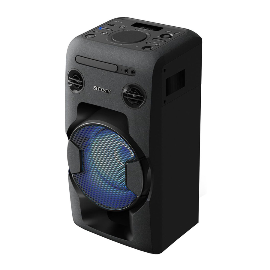
HOME AUDIO SYSTEM
US Model
Canadian Model
NEW
TDL-5W
General
Power requirements:
AC 120 V, 60 Hz
Power consumption:
45 W
Standby power consumption (at the
Standby Mode):
When BLUETOOTH standby mode is
set to off: 0.5 W (eco mode)
When BLUETOOTH standby mode is
set to on: 2.8 W (all wireless network
ports on)
Dimensions (W/H/D) (Approx.):
290 mm × 600 mm × 265 mm
Mass (Approx.):
Quantity of the system:
1 piece
Supplied accessories:
Remote control (1)
R03 (size AAA) batteries (2)
FM lead antenna (1)
AC power cord (1)
Design and specifications are subject to
change without notice.
Advertisement
Table of Contents

Related Manuals for Sony MHC-V11


Summary of Contents for Sony MHC-V11
- Page 1 10 kilohms Tuning range: 87.5 MHz 108.0 MHz (100 kHz step) Outputs AUDIO/PARTY CHAIN OUT L/R: oltage 2 V, impedance 600 ohms HOME AUDIO SYSTEM 9-896-262-01 Sony Video & Sound Products Inc. 2016A33-1 © 2016.01 Published by Sony Techno Create Corporation...
- Page 2 LES DIAGRAMMES SCHÉMATIQUES ET LA LISTE DES PIÈCES SONT CRITIQUES POUR LA SÉCURITÉ DE FONC- TIONNEMENT. NE REMPLACER CES COMPOSANTS QUE PAR DES PIÈCES SONY DONT LES NUMÉROS SONT DON- NÉS DANS CE MANUEL OU DANS LES SUPPLÉMENTS PUBLIÉS PAR SONY.
-
Page 3: Table Of Contents
MHC-V11 SECTION 1 SERVICING NOTES TABLE OF CONTENTS The SERVICING NOTES contains important information for servicing. Be sure to read this section before repairing the SERVICING NOTES unit..........NOTES ON HANDLING THE OPTICAL PICK-UP DISASSEMBLY BLOCK OR BASE UNIT 2-1. - Page 4 MHC-V11 HOW TO OPEN THE TRAY WHEN POWER SWITCH TURN OFF Note: Refer to “2. DISASSEMBLY” to remove the loader (CDM1) from the unit. gear loader (CDM1) 2 Draw out the tray. tray – Bottom view – 1 Rotate the gear in the...
-
Page 5: Disassembly
MHC-V11 SECTION 2 DISASSEMBLY • This set can be disassembled in the order shown below. 2-1. DISASSEMBLY FLOW When disassembling the unit, use the following jig for speaker removal. Part No. Description 2-2. LEFT SIDE COVER, J-2501-238-A JIG FOR SPEAKER REMOVAL... -
Page 6: Left Side Cover, Right Side Cover
MHC-V11 Note: Follow the disassembly procedure in the numerical order given. 2-2. LEFT SIDE COVER, RIGHT SIDE COVER 4 right side cover 1 screw 2 two screws 3 claw 1 screw 2 two screws 4 left side cover 3 claw... -
Page 7: Top Cover Block
MHC-V11 2-3. TOP COVER BLOCK front side front side This side is the terminal side. wire 3 two screws 4 screw – Left view – 2 connector (4P) (XP7) 1 FFC (20P) (XP10) 6 three claws 5 Lift up the top cover block in the direction of the arrow. -
Page 8: Main Volume Knob, Mic Volume Knob
MHC-V11 2-4. MAIN VOLUME KNOB, MIC VOLUME KNOB Note 1: The MIC volume knob can be removed even without remov- ing the main volume knob. 3 Insert a flathead screwdriver at both sides of the MIC volume knob and lift at the same time. -
Page 9: Control Board
MHC-V11 2-5. CONTROL BOARD 5 CONTROL board 1 seven screws 1 seven screws 1 four screws This side is the terminal side. 4 FFC (20P) top cover block (XP1) 3 connector (2P) (XP2) rear side 2 Lift up the CONTROL board block in the direction of the arrow. -
Page 10: Loader (Cdm1)
MHC-V11 2-7. LOADER (CDM1) 5 two screws 5 two screws 1 cushion 3 connector (6P) (XP5) 2 FFC (24P) (XP4) The opposite side is the terminal side. Wire cushion loader (CDM1) three hooks 4 connector (2P) (XP6) – – MAIN board... -
Page 11: Bt Board
MHC-V11 2-8. BT BOARD Note 1: When replacing the BT board, be sure to replace the BT board and the NFC board simultaneously. The BT board cannot re- place with single. Among the repair parts, the BT board and the NFC board is supplied as one unit. -
Page 12: Chassis Block
MHC-V11 2-9. CHASSIS BLOCK 3 three screws 2 screw wire front side 1 connector (7P) (XP11) 3 screw 3 screw 8 chassis block 7 connector (4P) (XP9) 6 connector (4P) (XP13) 4 rib 4 rib 5 connector (2P) (XP14) -
Page 13: Front Panel Block
MHC-V11 2-10. FRONT PANEL BLOCK 4 All bosses are removed while moving jig in the direction of total eleven bosses the arrow, and front panel block is removed. 1 three screws 3 Insert the jig into the space and slowly remove the front panel block. -
Page 14: Tweeter Unit Wire
MHC-V11 2-11. TWEETER UNIT WIRE 1 Push the protrusion, and remove the terminal (wide side). tweeter unit (R-ch) protrusion (SP3) front side front panel block 1 Push the protrusion, and remove the terminal (narrow side). protrusion short wire long wire... -
Page 15: Tweeter Unit (Sp2, Sp3)
MHC-V11 2-12. TWEETER UNIT (SP2, SP3) n tallation irection or t e tweeter nit Install so that the terminal (narrow side) of the tweeter unit aligns with the direction of the arrow. front side front panel block arrow – Front panel block rear view –... -
Page 16: Led A Board, Led B Board
MHC-V11 2-13. LED A BOARD, LED B BOARD front side front panel block groove groove 1 Draw the cable out of the groove. 1 Draw the cable out of the groove. groove 3 Remove the LED B board block in the direction of 5 cushion the arrow. -
Page 17: Woofer Unit (Sp1)
MHC-V11 2-14. WOOFER UNIT (SP1) Note: When installing the woofer unit (SP1), make the position of terminals as shown in the figure below. top side speaker cabinet block woofer unit (SP1) terminal position front side – Speaker cabinet block front view –... -
Page 18: Loader Block
MHC-V11 2-15. LOADER BLOCK 7 loader block 6 rib 6 rib 1 FFC (24P) (XP4) 2 connector (6P) (XP5) The opposite side is the terminal side. 3 connector (2P) (XP6) 5 three screws 4 three screws Wire e i loader (CDM1) -
Page 19: Main Board
MHC-V11 2-16. MAIN BOARD 3 screw 3 screw 3 screw 4 MAIN board 3 screw 2 screw 1 connector (9P) (XP2) front side chassis block 2-17. PSU BOARD 3 two screws 3 two screws groove hole 4 PSU board Note: When installing the PSU board,... -
Page 20: Test Mode
MHC-V11 SECTION 3 TEST MODE SOFTWARE VERSION DISPLAY It can confi rm the software version. Procedure: 1. Press the [ ] button to turn the power on. 2. Press the [FUNCTION] button to select the CD function. 3. Press the [ ] button to open the disc tray. -
Page 21: Electrical Checks
MHC-V11 SECTION 4 ELECTRICAL CHECKS TUNER SECTION 0 dB = 1 V CD SECTION Note: FM AUTO STOP CHECK 1. CD block is basically constructed to operate without adjustment. 2. Use YEDS-18 disc (Part No. 3-702-101-01) unless otherwise indicated. signal 3. -
Page 22: Diagrams
MHC-V11 SECTION 5 DIAGRAMS 5-1. BLOCK DIAGRAM - OVERALL Section - MHC-V11... -
Page 23: Block Diagram - Power Supply Section
MHC-V11 5-2. BLOCK DIAGRAM - POWER SUPPLY Section - MHC-V11... - Page 24 MHC-V11 THIS NOTE IS COMMON FOR PRINTED WIRING BOARDS AND SCHEMATIC DIAGRAMS. • Circuit Boards Location (In addition to this, the necessary note is printed in each block.) CONTROL board For Printed Wiring Boards. For Schematic Diagrams. Note: Note: • All capacitors are in μF unless otherwise noted. (p: pF) •...
-
Page 25: Printed Wiring Board - Main Board
MHC-V11 5-3. PRINTED WIRING BOARD - MAIN Board - • See page 24 for Circuit Boards Location. • : Uses unleaded solder. MAIN BOARD (COMPONENT SIDE) MAIN BOARD (CONDUCTOR SIDE) MHC-V11... -
Page 26: Schematic Diagram - Main Board (1/9)
MHC-V11 5-4. SCHEMATIC DIAGRAM - MAIN Board (1/9) - • See page 42 for IC Block Diagrams. MAIN BOARD (1/9) POWER INPUT SYSTEM_POWER & GND +12V V_12V AMP_36V C114 C114 C113 C113 PSON 100pF/50V/NP0 100pF/50V/NP0 0.1uF/50V/X7R 0.1uF/50V/X7R V_12V MAIN_36V P_AP2305 P_AP2305 0.1uF/25V/X5R... -
Page 27: Schematic Diagram - Main Board (2/9)
MHC-V11 5-5. SCHEMATIC DIAGRAM - MAIN Board (2/9) - MAIN BOARD (2/9) 3.3V_D2 100K 100K 27MHz/30PPM 27MHz/30PPM DEBUG_TX RF3.3V DEBUG_RX MCLK_1 MCLK_1 I2S_MCLK VCC1.2 AD_MCLK 30pF/50V/NP0 30pF/50V/NP0 39pF/50V/NP0 39pF/50V/NP0 4PIN/2.0mm 4PIN/2.0mm BCLK_1 BCLK_1 I2S_BCLK VCC1.2 AD_BCLK LRCLK_1 LRCLK_1 I2S_LRCK AD_LRCK... -
Page 28: Schematic Diagram - Main Board (3/9)
MHC-V11 5-6. SCHEMATIC DIAGRAM - MAIN Board (3/9) - • See page 42 for IC Block Diagrams. MAIN BOARD (3/9) S=H:2 ON 1 OFF SDRAM USB SWITCH S=L:1 ON 2 OFF SD33 C207 C207 NC/0.1uF/16V/X7R NC/0.1uF/16V/X7R STB_3.3V MA10 DQ10 A10/AP... -
Page 29: Schematic Diagram - Main Board (4/9)
MHC-V11 5-7. SCHEMATIC DIAGRAM - MAIN Board (4/9) - • See page 42 for IC Block Diagrams. MAIN BOARD (4/9) STB_5V MCU_3.3V MCU_3.3V STB_3.3V R117 R117 To LED board*2 R183 R183 R186 R186 MCU_RST R120 R120 SPK LED control R118... -
Page 30: Schematic Diagram - Main Board (5/9)
MHC-V11 5-8. SCHEMATIC DIAGRAM - MAIN Board (5/9) - • See page 42 for IC Block Diagrams. MAIN BOARD (5/9) LGRP MODE2 R175 R175 SRC_MCLK RCKI MODE1 MODE0 BT_DATA R176 R176 SRC_BCLK SDIN BCKO BT_BCLK R177 R177 C353 C353 C354... -
Page 31: Schematic Diagram - Main Board (6/9)
MHC-V11 5-9. SCHEMATIC DIAGRAM - MAIN Board (6/9) - MAIN BOARD (6/9) Reserved 3.3V_D1 3.3V_D1 R206 R206 VCC_D CE14 CE14 C171 C171 Audio IN FB25 FB25 R209 R209 R210 R210 500/200mA 500/200mA 4.7K 4.7K 4.7K 4.7K 4.7uF/10V/X5R 4.7uF/10V/X5R Analog_In_R C173... -
Page 32: Schematic Diagram - Main Board (7/9)
MHC-V11 5-10. SCHEMATIC DIAGRAM - MAIN Board (7/9) - • See page 42 for IC Block Diagrams. MAIN BOARD (7/9) FM_3.3V C235 330pF/50V/X7R C235 330pF/50V/X7R C236 C236 33pF/50V/NP0 33pF/50V/NP0 AGND XP12 XP12 VDDRF Y3 12MHz/20PPM Y3 12MHz/20PPM AGND FB26 FB26... -
Page 33: Schematic Diagram - Main Board (8/9)
MHC-V11 5-11. SCHEMATIC DIAGRAM - MAIN Board (8/9) - MAIN BOARD (8/9) YSS952 1.8V R320 R320 1.8V_D C255 C255 C256 C256 C257 C257 C258 C258 10uF/16V/X5R 10uF/16V/X5R MIC_DATA MIC_DATA_IN R325 R325 MIC_DATA I2S_DATA_OUT R327 R327 YSS_DATA_IN I2S_DATA_OUT 3.3V R328 R328... -
Page 34: Schematic Diagram - Main Board (9/9)
MHC-V11 5-12. SCHEMATIC DIAGRAM - MAIN Board (9/9) - • See page 42 for IC Block Diagrams. MAIN BOARD (9/9) AMP_36V CE20 CE20 C292 C292 0.1uF/50V/X7R 0.1uF/50V/X7R 820uF/50V 820uF/50V V_12V R376 R376 CE21 CE21 10 H/10A 10 H/10A Right C293 C293 0.1uF/50V/X7R... -
Page 35: Printed Wiring Board - Bt Board
MHC-V11 5-13. PRINTED WIRING BOARD - BT Board - 5-15. PRINTED WIRING BOARD - NFC Board - • See page 24 for Circuit Boards Location. • : Uses unleaded solder. • See page 24 for Circuit Boards Location. • : Uses unleaded solder. -
Page 36: Printed Wiring Board - Karaoke (Mic) Board
MHC-V11 5-17. PRINTED WIRING BOARD - KARAOKE (MIC) Board - • See page 24 for Circuit Boards Location. • : Uses unleaded solder. KARAOKE (MIC) BOARD (COMPONENT SIDE) KARAOKE (MIC) BOARD (CONDUCTOR SIDE) 5-18. SCHEMATIC DIAGRAM - KARAOKE (MIC) Board -... -
Page 37: Printed Wiring Board - Led A Board
MHC-V11 5-19. PRINTED WIRING BOARD - LED A Board - 5-21. PRINTED WIRING BOARD - LED B Board - • See page 24 for Circuit Boards Location. • : Uses unleaded solder. • See page 24 for Circuit Boards Location. -
Page 38: Printed Wiring Board - Control Board
MHC-V11 5-23. PRINTED WIRING BOARD - CONTROL Board - • See page 24 for Circuit Boards Location. • : Uses unleaded solder. CONTROL BOARD (COMPONENT SIDE) CONTROL BOARD (CONDUCTOR SIDE) MHC-V11... -
Page 39: Schematic Diagram - Control Board
MHC-V11 5-24. SCHEMATIC DIAGRAM - CONTROL Board - CONTROL BOARD +12V VFD1 VFD1 Green Vacuum Fluorescent Display 100 Green Vacuum Fluorescent Display 100 To main board +5VA 47uF/50V 47uF/50V NPN_3DG3904M NPN_3DG3904M NPN_3DG3904M NPN_3DG3904M 500/800mA 500/800mA STB_5V_LED 0.1uF/50V/X7R 0.1uF/50V/X7R 3.3uF/50V 3.3uF/50V... -
Page 40: Printed Wiring Board - Psu Board
MHC-V11 5-25. PRINTED WIRING BOARD - PSU Board - • See page 24 for Circuit Boards Location. • : Uses unleaded solder. PSU BOARD PSU BOARD (COMPONENT SIDE) (CONDUCTOR SIDE) MHC-V11... -
Page 41: Schematic Diagram - Psu Board
MHC-V11 5-26. SCHEMATIC DIAGRAM - PSU Board - PSU BOARD D542 D542 HER203G/2A/200V HER203G/2A/200V T501 T501 R510 R510 NC/2.2/2W NC/2.2/2W PQ3230 PQ3230 C510 C510 R580 R580 R514 R514 8.2/2W 8.2/2W 2200pF/1KV 2200pF/1KV M36V M36V R5101 R5101 R509 R509 R5102 R5102... - Page 42 MHC-V11 • IC Block Diagrams – MAIN Board – U1 EUP3490 U4 SY8089A U2 EUP3504 U10 G527 Output Reverse-Voltage Output Reverse-Voltage Protection Protection NMOS NMOS Switch Switch FLAG FLAG Under Under Over-Temperature Over-Temperature Charge Charge Voltage Voltage Protection Protection Pump...
- Page 43 MHC-V11 U13 STM32F030R8T6 Serial POWER DD18 SWCLK Wire VOLT.REG = 2.4 to 3.6 V SWDIO Debug 3.3 V TO 1.8 V as AF Flash up to 64 KB, CORTEX-M0 CPU SUPPLY 32 bits = 48 MHz Reset SUPERVISION HCLK NRST...
- Page 44 MHC-V11 U14 SRC4182 U25 RZ5B705...
- Page 45 MHC-V11 U28 TAS5534 Output Control 2 Crossbar Mixer 8 Crossbar Mixer AVSS AVDD DVSS DVDD DAP Control PWM Control VRD_PLL VRA_PLL VBGAP System Control AVDD_REF AVSS_PLL AVDD_PLL VR_PLL Clock, PLL, and Serial Data I/F...
- Page 46 MHC-V11 U29 TAS5624A /CLIP /OTW /FAULT BST_X GVDD_X AVDD DVDD /RESET MODE1-3 POWER-UP RESET AVDD AVDD TEMP SENSE DVDD CB3C OVER- DVDD LOAD PROTECTION STARTUP CONTROL C_START BST_A PVDD_AB INPUT_A PWM & RECEIVER ANALOG TIMING GATE-DRIVE OUT_A LOOP FILTER CONTROL...
-
Page 47: Exploded Views
MHC-V11 SECTION 6 EXPLODED VIEWS Note: • -XX and -X mean standardized parts, so • The mechanical parts with no reference The components identifi ed by mark 0 they may have some difference from the number in the exploded views are not sup- or dotted line with mark 0 are critical for original one. -
Page 48: Top Cover Section
MHC-V11 6-2. TOP COVER SECTION Included in Ref. No. 102 on page 49. NFC board (See Note) not supplied FFC1 not supplied not supplied not supplied not supplied not supplied not supplied Note: When replacing the NFC board, be sure to replace the BT board (Ref. -
Page 49: Woofer Unit Section
MHC-V11 6-3. WOOFER UNIT SECTION not supplied not supplied not supplied not supplied main section not supplied not supplied supplied not supplied not supplied not supplied FFC2 not supplied not supplied not supplied supplied supplied not supplied not supplied not supplied... -
Page 50: Front Panel Section
MHC-V11 6-4. FRONT PANEL SECTION • Rear side view not supplied not supplied not supplied not supplied not supplied not supplied not supplied not supplied not supplied not supplied not supplied not supplied not supplied not supplied Ref. No. Part No. -
Page 51: Main Section
MHC-V11 6-5. MAIN SECTION not supplied not supplied not supplied CDM1 supplied not supplied not supplied not supplied not supplied not supplied not supplied supplied not supplied supplied supplied not supplied not supplied not supplied not supplied not supplied supplied... -
Page 52: Accessories
MHC-V11 SECTION 7 ACCESSORIES Ref. No. Part No. Description Remark 4-582-493-11 MANUAL, INSTRUCTION (ENGLISH, FRENCH, SPANISH) 9-885-189-79 FM ANTENNA (FM lead antenna) 0 502 9-885-209-20 AC CORD (AC power cord) 1-493-171-11 REMOTE COMMANDER (RMT-AM220U) (Remote control) The components identifi ed by mark 0 or dotted line with mark 0 are critical for safety. - Page 53 MHC-V11 MEMO...
- Page 54 MHC-V11 REVISION HISTORY Ver. Date Description of Revision 2016.01...
Need help?
Do you have a question about the MHC-V11 and is the answer not in the manual?
Questions and answers
Finale audio che montato? Input output? Grazie