Table of Contents
Advertisement
Quick Links
SERVICE MANUAL
MODEL
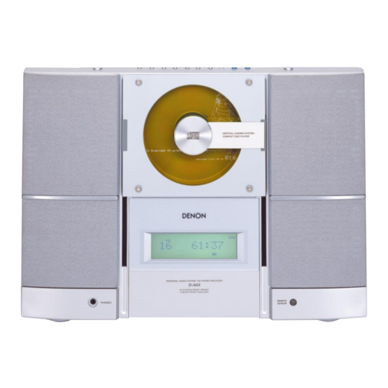
PERSONAL AUDIO SYSTEM
VERTICAL LOADING SYSTEM
COMPACT DISC PLAYER
PERSONAL AUDIO SYSTEM/CD-MD RECEIVER
D-A03
MENU
TUNING
SLEEP TIMER
OFF TOTAL
RANDOM INTOR SCAN ROCK POP JAZZ DANCE FLATT
power loading mechanism
PHONES
REMOTE
SENSOR
Hong Kong model
G G G G G
Some illustrations using in this service manual are slightly different from the actual set.
14-14, AKASAKA 4-CHOME, MINATO-KU, TOKYO 107-8011 JAPAN
D-A03
POWER
C D
FM/AM
M D
AUX
VOLUME
TUNING/
PRESET
N.SPEED
HI.SPEED
SDB
REC
REC MODE
E Q
TOC/NAME
ENTER
CLEAR
DISPLAY
TIMER/DELETE
PLAY MODE
PHONES
PROG.
REMOTE CONTROL UNIT
Telephone: 03 (3584) 8111
For Hong Kong,
U.S.A. and Canada model
Hi-Fi Personal Audio System
VERTICAL LOADING SYSTEM
COMPACT DISC PLAYER
PERSONAL AUDIO SYSTEM / CD STEREO RECEIVER
40-STATION PRESET MEMORY
6-MODE PRESET EQUALIZER
REMOTE
SENSOR
U.S.A. and Canada model
POWER
C D
SDB
FM/AM
AUX
EQ
VOLUME
TUNING/
PRESET
REMOTE CONTROL UNIT
X0130 337 NC 0112
Advertisement
Table of Contents
Troubleshooting

Subscribe to Our Youtube Channel
Related Manuals for Denon D-A03


Summary of Contents for Denon D-A03
- Page 1 For Hong Kong, U.S.A. and Canada model Hi-Fi Personal Audio System SERVICE MANUAL D-A03 MODEL PERSONAL AUDIO SYSTEM VERTICAL LOADING SYSTEM VERTICAL LOADING SYSTEM COMPACT DISC PLAYER COMPACT DISC PLAYER POWER POWER PERSONAL AUDIO SYSTEM/CD-MD RECEIVER FM/AM D-A03 FM/AM MENU...
-
Page 2: Safety Precautions
D-A03 SAFETY PRECAUTIONS The following check should be performed for the continued protection of the customer and service technician. LEAKAGE CURRENT CHECK Before returning the unit to the customer, make sure you make either (1) a leakage current check or (2) a line to chassis resistance check. - Page 3 D-A03 DISASSEMBLY (Follow the procedure below in reverse order when reassembling) 1. Rear Cover & Front Panel 1) Remove 14 rear screws and 4 (E3: 2) bottom screws on the Rear Cover. 2) Disconnect connectors and wire on the Front Panel.
- Page 4 D-A03 3. MD Mecha. 1) Remove 3 screws Connector 2) Disconnect 1 each FFC and connector on the Main P.W.B. MD Mecha. 4. CD Mecha. Chassis 1) Remove 4 each screws from the front side to detach the CD Door Lens and CD Door Bracket.
- Page 5 D-A03 Speaker Box (L) 6. Speaker Box (L & R) 1) Remove 4 screws " 2) Disconnect 2 connectors. Speaker Box (R) " " 7. Tuner P.W.B. 1) Remove 2 screws Tuner P.W.B. 8. Power P.W.B. 1) Remove 6 screws 2) Disconnect 1 connector.
- Page 6 D-A03 ADJUSTMENT TUNER SECTION Connections and adjustment point Modulation frequency: 400Hz AM SG Modulation factor: 30% Modulation frequency: 1kHz Test loop antenna L+R: 90% (67.5kHz Dev.) Pilot: 10% (7.5kHz Dev.) 75kHz Dev.: 100% 60cm FM stereo modulator 75 ohms Loop antenna...
- Page 7 D-A03 CD SECTION 1. RF level Confieming Connection Oscilloscope CD Servo Micon PWB Probe 10:1 − Oscilloscope Check Step 1. Press CD Play/Pause ( ) button 0.2µs/div to make it playback state. 50mV/div 2. Check RF level with oscilloscope. 0.5µs/div 3.
- Page 8 D-A03 BLOCK DIAGRAM TACT KEY REMOTE Sensor CD DOOR Door driver DISPLAY UNIT BA6286 MAIN UNIT 8com,60seg MICRO Motor driver COMPUTER CD MECHA LA6558 BACK light TC94A14FA M38199 CD4LXWNK RF AMP TA2157F Controller LC75811W Reset 74VHC08 MD UNIT MDM08AD ELE.VR SYSTEM...
- Page 9 D-A03 TEST MODE (There is no MD Section in the U.S.A. and Canada model) From power off state to TEST mode To enter into the TEST mode, plug the AC cord to the wall outlet while pressing the CD PLAY (CD ) button and TUNER button simultaneously.
- Page 10 D-A03 1. CD test Outline: Readout of the set value after automatic adjustment (for judging difference from initial value) Forced operation of pickup (Inner/Outer circumference feed) During the PLAY mode, the number of errors accumulated for 10 seconds (750 frames) is displayed.
- Page 11 D-A03 Double-speed mode Press the MD-REC button in the stop mode to switch to the double/constant-speed mode cyclically. During the double-speed mode, lights up. CD TEST N:NORMAL SPEED STEP NO Display TNO Display H:HIGH SPEED Time Display Lights when double-speed mode...
- Page 12 D-A03 MD SECTION Enter the test mode, adjust or set as shown in the following table according to the repair operations. Execution item TEMP Checking Writing the Writing the AUTO-YOBI AUTO- AUTO-AFB required basic EEPROM EEPROM EEPROM Operation check adjustment...
- Page 13 D-A03 Entering the specific mode Whenever the CD PLAY (CD ) button is pressed, the mode is changed. If the REC button is pressed instead, the mode will change in the opposite order. AUT YOBI AUTO AJST AUT AFB RST YOBI...
- Page 14 D-A03 2. AUTO pre-adjustment mode (Low reflection disc only) Step No. Setting Method Remarks Display Step 1 Test mode stop status Step 2 Press once the CD PLAY button Auto adjustment menu AUTO_AJST_ Step 3 Press REC button Auto pre-adjust menu...
- Page 15 D-A03 5. EEPROM Setting Mode A) Focus Setting Step No. Setting Method Display Step 1 Test mode stop status Step 2 Press CD PLAY button 8 times EEPROM_SET Step 3 Press MD PLAY button _ _Focus_ _ _ _ Step 4...
- Page 16 D-A03 C) Tracking Setting Step No. Setting Method Display Step 1 Test mode stop status Step 2 Press CD PLAY button 8 times EEPROM_SET Step 3 Press MD PLAY button _ _Focus_ _ _ Step 4 Press CD PLAY button 2 times...
- Page 17 D-A03 D) Slide Setting Step No. Setting Method Display Step 1 Test mode stop status Step 2 Press CD PLAY button 8 times EEPROM_SET Step 3 Press MD PLAY button _ _Focus_ _ _ _ Step 4 Press CD PLAY button 3 times...
- Page 18 D-A03 G) Adjust Setting Step No. Setting Method Display Step 1 Test mode stop status Step 2 Press CD PLAY button 8 times EEPROM_SET Step 3 Press MD PLAY button _ _Focus_ _ _ Step 4 Press CD PLAY button 6 times...
- Page 19 D-A03 6. Test-play Mode (For checking playback performance at the address defined.) Step No. Setting Method Remarks Display Step 1 Test mode stop status Step 2 Press TUNER button Test-play menu TEST_PLAY_ Step 3 Press CD STOP button Address setting (displays address initial value)
- Page 20 D-A03 Lead-in SW Position Measurement Mode 1. Adjustment Load the high reflection test disc TGYS1. Note: Adjust the lead-in switch position to FF85 ~ FFD2. 1. Loosen 1 screw (A1) fixing the Mecha. SW P.W.B. 2. Loosen the screw once and retighten it with pushing the P.W.B.
- Page 21 D-A03 Detailed Description of Error Indication Error Indication Content of Error Remedy Can't REC DEFECT occured continuously for 10 times during Is there any scratch, dust, finger print, black spot, etc. on REC-PLAY the disc? Check for eccentricity, warp, etc. of disc.
- Page 22 D-A03 Error Indication Content of Error Remedy Can't WRITE As abnormality occurred during UTOC rewriting, unable Scratch, etc. on the disc. Replace with the other disc. to perform correct rewriting. Unable to lead in FOCUS as the disc is inserted.
-
Page 23: Eeprom Writing Procedure
D-A03 EEPROM WRITING PROCEDURE EEPROM (IC1402) writing procedure 1. Method for setting the reference temperature value (This setting should be performed quickly at a room temperature, between 21 to 29 when the PWB is not hot.) 1) When replacing the EEPROM, wait until it has cooled down. - Page 24 D-A03 Table of EEPROM Contents (Version: 01) (a) Focus Setting (c) Tracking Setting Item Setting Item Setting FG______$$ TG______$$ FG2_____$$ TG2_____$$ FF0_____$$ TF0_____$$ FF1_____$$ TF1_____$$ FF2_____$$ TF2_____$$ FZHLEV__$$ FT3_____$$ FOKLEVh_$$ SVCNT4__$$ FOKLEVt_$$ TRBLVo__$$ FOSTn___$$ TRBLVt__$$ DSCJG__$$ TRKLVo__$$ TRKLVt__$$ TDPWo___$$ (b) Spindle Setting...
- Page 25 D-A03 (d) Slide Setting (e) Control Setting (f) ADJSET Display Setting Display Setting Display Setting CONTRL1_$ $ SLG_____$$ COK___$$ SL2_____$$ CONTRL2_$$ FAT___$$ SLDLIM__$$ ADJTTM__$$ TAT___$$ SLDLEV__$$ HDEQAD__$$ CAT___$$ SLKLVk__$$ LDEQAD__$$ FAB___$$ SLKLVt__$$ GDEQAD__$$ STR___$$ SLKLVm__$$ GDEQAD2_$$ SFS___$$ SLBKm__$$ HDEQBC__$$ STC___$$...
- Page 26 D-A03...
- Page 27 D-A03 TROUBLESHOOTING OF CD CD SECTION When the CD does not function When the CD section does not operate when the objective lens of the optical pickup is dirty, this section may not operate. Clean the objective lens, and check the playback operation. When this section does not operate even after the above step is taken, check the following items.
- Page 28 D-A03 The laser does not light up Is 1.5V applied to the LDO terminal of pin 7 of IC146 ? IC146 is defective Is +1.8V applied to the collector of TR101 ? Is +3.3V applied to C109 of R108 ? R108 is defective.
- Page 29 D-A03 The triangular wave for focus servo does not appears Is +3.3V applied to pin 6 of IC149 ? The +3.3V line of IC149 is defective. Does the triangular wave appear at pin 33 on IC149 ? Check the parts around pin 33 on IC149. If OK, IC149 is <Refer to the waveform diagrams on page 32.>...
- Page 30 D-A03 No sound is heard Is the digital signal outputted from the pin 4 (digital OUT) of Check the parts around IC149. If OK, IC149 is defective. IC149 ? Is digital signal outputted from the pin 8 (digital OUT) of Check the parts around IC150.
-
Page 31: Waveforms Of Cd Circuit
D-A03 WAVEFORMS OF CD CIRCUIT Tracking error Foucus servo on 2000/09/18 15:29:21 Stopped Stopped 2000/09/18 16:56:26 CH1=500mV CH2=2V CH3=2V 2ms/div CH1=200mV 5ms/div DC 10:1 DC 10:1 DC 10:1 (2ms/div) DC 10:1 (5ms/div) NORM:500kS/s NORM:200kS/s IC146 15pin Disc playback When there is no When a door wound in the disc. - Page 32 D-A03 Feed motor and tracking output during the track jump Normal track actuator drive Stopped 2000/09/18 17:12:20 Stopped 2000/09/18 17:16:55 CH1=200mV 100ms/div CH2=1V CH1=1V 500us/div DC 10:1 DC 10:1 (100ms/div) DC 10:1 (500us/div) NORM:10kS/s NORM:2MS/s When there is no track jump wound in the disc.
- Page 33 D-A03 TROUBLESHOOTING OF MD (Hong Kong model) When MD Inoperative Clean the object lens first then check the playback function because no operation may be caused by dirty object lens of the optical pickup. Follow the steps below if it's still inoperative after the cleaning. When the object lens is unclean with dust or etc., problems such as skipping or no TOC indication may happen.
- Page 34 D-A03 Disc Loading Not Normal When disc insertion, does the loading operation start ? Is the voltage at 17, 18pin of CN1501 +5.0 ~ +6.0V ? Check Power, System PWB, and CN1501. When reset power on, does pulse signal enter into 6pin of Check System PWB and CN1501.
- Page 35 D-A03 Recording/playback Operation Set to Rec/play Test Mode after confirming audio output at playback with low ref. disc insertion. No recording from the start address. Isn't the disc set to record prohibited position ? Is there RF waveform at TP1201 or 1pin of IC1201(Mecha.) when playback after recording ?
- Page 36 D-A03 WAVEFORMS OF MD CIRCUIT (Hong Kong model)
- Page 37 D-A03...
- Page 38 Clock for LC75811W P56/SOUT3/AN13 LCD_DI Data output for LC75811W P54/SIN3/AN12 Distinction between DENON & W products, L: DENON P53/SRDY2/AN11 MD_LOAD_SW MD LOAD SW detect, L→H: DISC IN P52/SCLK2/AN10 MD_ST 20ms H at CD music start, 100ms H at MD ON...
- Page 39 D-A03 Voltage Pin Name Symbol Function XOUT X_OUT Osc. output 8.38MHz GND GND Surround Surround ON/OFF, H: ON /CD_PU_IN CD PU inner most detect, L: Inner most /DR_OP_IN CD DOOR open switch detect, L: OPEN /DR_CL_IN CD DOOR close switch detect, L: CLOSE...
- Page 40 D-A03 TC94A14FA (IC149) TEZI Clock generator SBAD 1-bit Servo control RFRP RFZI ZDET RFCT Digital equalizer Address automatic circuit adjustment circuit BUS0 Data CLV servo slicer BUS1 SLCO BUS2 Synchronous guarantee BUS3 VCOF decoder Audio out Digital output BUCK circuit...
- Page 41 D-A03 Symbol Function SBSY Subcode block sync signal output pin. General-purpose input/output pins. Input port at reset. PLL-only 3.3V power supply voltage pin. EFM and PLCK phase difference signal output pin. TMAX TMAX detection result output pin. LPFN Inverted input pin for PLL LPF amp.
- Page 42 D-A03 LA6558 (IC145) VO3- VO6+ VO3+ VO6- VO5- VO2+ VO5+ VO2- VO4- VO1+ VO4+ VO1- Power System P-GND1 P-GND2 Power System GND S-GND P-VCC(IN) Signal System GND Power System VCC VREF 3.3VREG(OUT) 3.3VREG Reference Voltage Signal System VCC IN-MUTE MUTE...
- Page 43 D-A03 TA2157F (IC146) TA2157F Terminal Function Voltage Description Symbol 3kΩ 3.3 power pin 3kΩ Main beam amp input 1.65 22kΩ 40pF Main beam amp input 1.65 94kΩ 180kΩ 60kΩ Sub beam amp input 1.65 22kΩ Sub beam amp input 1.65...
- Page 44 D-A03 LA1844 (IC402) RF. AM DECODER BUFF PILOT ANTI-BIRDIE CANCEL STEREO φ AM/FM LEVEL VIEW COMP S-CURVE π PILOT ∠ ∠ 304kHz TUNING DRIVE LA1844 Terminal Function Voltage Voltage Pin No. Function Pin No. Function FM IF input 2.34 L output 3.17...
- Page 45 D-A03 LC72131M (IC401) BA6286 (IC151) CONTROL LOGIC XOUT POWER SAVE FRONT VIEW AOUT BA5415A (IC707) FRONT VIEW FMIN AMIN T.S.D IFIN 74VHC08F (IC150) BA08ST (IC703) BA15218F (IC605) BA10ST (IC701) V cc FRONT VIEW N.C. Output:Open Collector NJM7805FA (IC702) M51957FP (SY1) NJM7806FA (IC704) 5µA...
- Page 46 D-A03 DIODES 1N4004 MTZJ5P6B SVC321SP 1N4148 MTZJ6P2A FRONT VIEW 1N5404 MTZJ7P5A REMOTE CONTROL SENSOR IC PROTECTOR RPM6938-V4 (IC604) ICP-N10T (IC152,153) TOP VIEW FRONT VIEW LC DISPLAY TSB0716-UGTDPW (FL501) Pin Connection Pin No. 9 10 11 12 13 14 15 16 17 18 19 20 21 22 23 24 25 26 27 28 29 30 31 32 33 34 Connection Pin No.
- Page 47 D-A03 PRINTED WIRING BOARDS MAIN P .W.B. UNIT Ass'y COMPONENT SIDE...
- Page 48 D-A03 MAIN P .W.B. UNIT Ass'y 17 16 48 49 FOIL SIDE...
- Page 49 D-A03 DISPLAY P .W.B. UNIT Ass'y COMPONENT SIDE FOIL SIDE...
- Page 50 D-A03 NOTE FOR PARTS LIST Part indicated with the mark " " are not always in stock and possibly to take a long period of time for supplying, or in some case supplying of part may be refused. When ordering of part, clearly indicate "1" and "I" (i) to avoid mis-supplying.
- Page 51 D-A03 PARTS LIST OF P.W.B. UNIT ASS'Y Note : The symbols in the column “Remarks” indicate the following destinations. E1H: Hong Kong model MAIN P.W.B. UNIT ASSY E3 : U.S.A. & Canada model Ref. No. Part No. Part Name Remarks Ref.
- Page 52 D-A03 Ref. No. Part No. Part Name Remarks Ref. No. Part No. Part Name Remarks R141 951 9002 655 Carbon chip 150 kohm 1/16W R419 951 9002 956 Carbon chip 7.5 kohm 1/16W R142 951 9002 927 Carbon chip 5.6 kohm 1/16W...
- Page 53 D-A03 Ref. No. Part No. Part Name Remarks Ref. No. Part No. Part Name Remarks R620,621 951 9002 684 Carbon chip 1 kohm 1/16W R719,720 951 9002 684 Carbon chip 1 kohm 1/16W R622 951 9002 794 Carbon chip 2.2 kohm 1/16W...
- Page 54 D-A03 Ref. No. Part No. Part Name Remarks Ref. No. Part No. Part Name Remarks C152 951 9001 928 Ceramic chip 0.033uF/50V C406 951 9003 379 Electrolytic 10uF/25V C153 951 9001 931 Ceramic chip 0.047uF/50V C409 951 9001 915 Ceramic chip 0.022uF/50V C154 951 9003 586 Ceramic chip 0.068uF/16V...
- Page 55 D-A03 Ref. No. Part No. Part Name Remarks Ref. No. Part No. Part Name Remarks C479 951 9001 753 Ceramic chip 22pF/50V C801-804 951 9003 719 Electrolytic 47uF/25V C480 951 9003 395 Electrolytic 100uF/16V C805,806 951 9002 516 Mylar film 0.22uF/50V...
- Page 56 D-A03 Ref. No. Part No. Part Name Remarks Q'ty Ref. No. Part No. Part Name Remarks Q'ty 951 0069 600 4P antenna terminal for E3 951 0070 408 Rubber for E1H JK301 951 0059 801 Mini jack UL PVC tube (1) for E1H ...
- Page 57 D-A03 DISPLAY P.W.B. UNIT ASSY Ref. No. Part No. Part Name Remarks SEMICONDUCTORS GROUP IC501 951 0023 400 IC LC75811W D501 GP3 8002 006 Diode 1N4148 RESISTORS GROUP R501 951 0025 204 Metal oxide 2.2 ohm 1W R502 951 9002 820 Carbon chip 33 kohm 1/16W R503 951 9002 859 Carbon chip 3.3 kohm 1/16W...
- Page 58 D-A03 EXPLODED VIEW WARNING: Parts marked with this symbol have critical characteristics. Use ONLY replacement parts recommended by the manufacturer. FOR E3 102A FOR E1H 101A FOR E1H FOR E1H FOR E1H Note : The symbols indicate the FOR E3 following destinations.
- Page 59 D-A03 ( There is no MD section in the U.S.A. and Canada model. ) Note : The symbols in the column “Remarks” indicate the following destinations. PARTS LIST OF EXPLODED VIEW E1H : Hong Kong model E3 : U.S.A. & Canada model Ref.
- Page 60 D-A03 EXPLODED VIEW OF MD MECHANISM (Hong Kong model)
- Page 61 D-A03 PARTS LIST OF MD MECHANISM (For Hong Kong model) Ref. No. Part No. Part Name Remarks Q'ty 2 937 0246 207 Drive Chassis (A) 3 937 0246 304 Drive Chassis (B) 4 937 0279 300 Cartridge Holder Ass’y 5 937 0247 400 Slider Lever Ass’y...
- Page 62 D-A03 ADDEMDUM PARTS LIST OF MD MECHANISM Note: All parts, except for the following, are the same that of MAIN P.W.B. UNIT ASS’Y (MDM08AD) (For Hong Kong model) used of DMD-M50(MDM08A). Ref. No. Part No. Part Name Remarks SEMICONDUCTORS GROUP...
- Page 63 D-A03 PACKING VIEW Note : The symbols in the column “Remarks” indicate the following destinations. PARTS LIST OF PACKING & ACCESSORIES E1H : Hong Kong model E3 : U.S.A. & Canada model Ref. No. Part No. Part Name Remarks Q'ty Ref.
- Page 64 D-A03 WIRING DIAGRAM Japanese 100V AC 115V-230V 120V 50/60Hz 50Hz 60Hz CORD HOLDER POWER TRANS EARTH WIRE CX034 CY111 POWER/AMP P .W.B. L-out R-out F701 F702 CX035 TO SPEAKER 2.5A~250V 4A~125V POWER KEY CY061 P .W.B. OPEN/CLOSE KEY FUNCTION-KEY W104 P .W.B.
- Page 65 D-A03 SCHEMATIC DIAGRAMS (1/5) E1H(1~600) E3, E1H(601~) R387, 388 8.2K R319, 320 10K TR305, 306 OPEN DTC323TK R321, 322 OPEN R369 OPEN C341, 342 47/50 4.7/50 R365, 366 100K 4.8V 9.7V 4.8V R635 10K OPEN R693 OPEN 10K 1.3V WARNING Parts marked with this symbol have critical characteristics.
- Page 66 D-A03 SCHEMATIC DIAGRAMS (2/5) WARNING NOTICE ALL RESISTANCE VALUES IN OHM. k=1,000 OHM M=1,000,000 OHM Parts marked with this symbol have critical characteristics. correspond to the waveform numbers Use ONLY replacement parts recommended by the manufacture. ALL CAPACITANCE VALUES IN MICRO FARAD. P=MICRO-MICRO FARAD shown in pages 36 to 37.
- Page 67 D-A03 SCHEMATIC DIAGRAM (3/5) R805,806 4.3K +10V +5.5V F701 T4A/250V 4A/125V F702 T2.5/250V 2.5/250V SIGNAL LINE WARNING: Parts marked with this symbol have critical characteristics. Use ONLY replacement parts recommended by the manufacture. NOTICE CAUTION: ALL RESISTANCE VALUES IN OHM. k=1,000 OHM M=1,000,000 OHM...
- Page 68 D-A03 SCHEMATIC DIAGRAM (4/5) WARNING: Parts marked with this symbol have critical characteristics. Use ONLY replacement parts recommended by the manufacture. NOTICE CAUTION: ALL RESISTANCE VALUES IN OHM. k=1,000 OHM M=1,000,000 OHM Before returning the unit to the customer, make sure you make either (1) a SCHEMATIC DIAGRAM (4/5) leakage current check or (2) a line to chassis resistance check.
- Page 69 D-A03 SCHEMATIC DIAGRAM (5/5) WARNING: SIGNAL LINE Parts marked with this symbol have critical characteristics. Use ONLY replacement parts recommended by the manufacture. CAUTION: NOTICE Before returning the unit to the customer, make sure you make either (1) a ALL RESISTANCE VALUES IN OHM. k=1,000 OHM M=1,000,000 OHM ALL CAPACITANCE VALUES IN MICRO FARAD.
Need help?
Do you have a question about the D-A03 and is the answer not in the manual?
Questions and answers