Advertisement
Quick Links
QQ
3 7 63 1515 0
TE
L 13942296513
●
For purposes of improvement, specifications and
design are subject to change without notice.
●
Please use this service manual with referring to
the operating instructions without fail.
●
Some illustrations using in this service manual are
slightly different from the actual set.
www
.
http://www.xiaoyu163.com
SERVICE MANUAL
MODEL
PERSONAL AUDIO SYSTEM
x
ao
u163
y
i
16-11, YUSHIMA 3-CHOME, BUNKYOU-KU, TOKYO 113-0034 JAPAN
http://www.xiaoyu163.com
2 9
8
For U.S.A. & Canada model
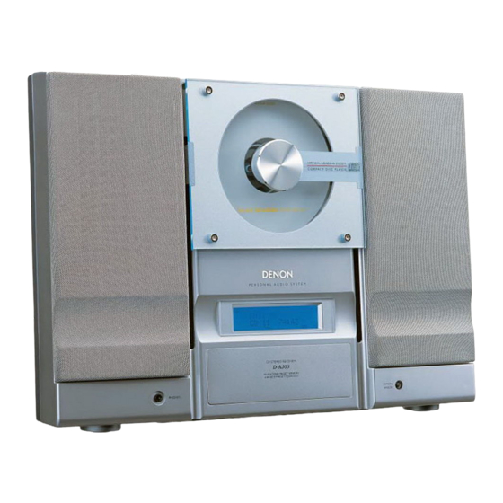
D-AJ03
Q Q
3
6 7
1 3
1 5
注 意
サービスをおこなう前に、このサービスマニュアルを
必ずお読みください。本機は、火災、感電、けがなど
に対する安全性を確保するために、さまざまな配慮を
おこなっており、また法的には「電気用品安全法」に
もとづき、所定の許可を得て製造されております。
従ってサービスをおこなう際は、これらの安全性が維
持されるよう、このサービスマニュアルに記載されて
いる注意事項を必ずお守りください。
● 本機の仕様は性能改良のため、予告なく変更すること
があります。
● 補修用性能部品の保有期間は、製造打切後 8年です。
●
修理の際は、必ず取扱説明書を参照の上、作業を行って
ください。
● 本文中に使用しているイラストは、説明の都合上現物
と多少異なる場合があります。
co
.
9 4
2 8
Ver. 1
0 5
8
2 9
9 4
2 8
,
m
X0178V.01 DE/CDM 0307
9 9
9 9
Advertisement

Related Manuals for Denon D-AJ03


Summary of Contents for Denon D-AJ03
- Page 1 3 7 63 1515 0 For U.S.A. & Canada model Ver. 1 SERVICE MANUAL D-AJ03 MODEL PERSONAL AUDIO SYSTEM L 13942296513 注 意 サービスをおこなう前に、このサービスマニュアルを 必ずお読みください。本機は、火災、感電、けがなど に対する安全性を確保するために、さまざまな配慮を おこなっており、また法的には「電気用品安全法」に もとづき、所定の許可を得て製造されております。 従ってサービスをおこなう際は、これらの安全性が維 持されるよう、このサービスマニュアルに記載されて いる注意事項を必ずお守りください。 ● ● 本機の仕様は性能改良のため、予告なく変更すること For purposes of improvement, specifications and design are subject to change without notice.
-
Page 2: Safety Precautions
D-AJ03 SAFETY PRECAUTIONS 3 7 63 1515 0 The following check should be performed for the continued protection of the customer and service technician. LEAKAGE CURRENT CHECK Before returning the unit to the customer, make sure you make either (1) a leakage current check or (2) a line to chassis resistance check. - Page 3 D-AJ03 3 7 63 1515 0 DISASSEMBLY (Follow the procedure below in reverse order when reassembling) 1. Rear Cover & Front Panel 1) Remove 14 rear screws and 4 (E3: 2) bottom screws on the Rear Cover. 2) Disconnect connectors and wire on the Front Panel.
- Page 4 D-AJ03 3 7 63 1515 0 3. CD Mecha. Chassis 1) Remove 4 each screws from the front side to ı ı ı detach the CD Door Lens and CD Door Bracket. 2) Remove 6 screws and take off the Main Chassis.
- Page 5 D-AJ03 3 7 63 1515 0 Speaker Box (L) 5. Speaker Box (L & R) 1) Remove 4 screws ı 2) Disconnect 2 connectors. Speaker Box (R) ı ı 6. Tuner P.W.B. 1) Remove 2 screws ı L 13942296513 Tuner P.W.B.
-
Page 6: Tuner Section
D-AJ03 3 7 63 1515 0 ADJUSTMENT TUNER SECTION Connections and adjustment point Modulation frequency: 400Hz AM SG Modulation factor: 30% Modulation frequency: 1kHz Test loop antenna L+R: 90% (67.5kHz Dev.) Pilot: 10% (7.5kHz Dev.) 75kHz Dev.: 100% 60cm... - Page 7 D-AJ03 3 7 63 1515 0 CD SECTION 1. RF level Confieming Connection Oscilloscope CD Servo Micon PWB Probe 10:1 Oscilloscope Check Step 1. Press CD Play/Pause ( ) button 0.2 s/div to make it playback state. 50mV/div 2. Check RF level with oscilloscope.
- Page 8 D-AJ03 BLOCK DIAGRAM 3 7 63 1515 0 L 13942296513 u163 http://www.xiaoyu163.com...
-
Page 9: Test Mode
D-AJ03 3 7 63 1515 0 TEST MODE From power off state to TEST mode To enter into the TEST mode, plug the AC cord to the wall outlet while pressing the CD PLAY (CD ) button and TUNER button simultaneously. - Page 10 D-AJ03 3 7 63 1515 0 1. CD test Outline: Readout of the set value after automatic adjustment (for judging difference from initial value) Forced operation of pickup (Inner/Outer circumference feed) During the PLAY mode, the number of errors accumulated for 10 seconds (750 frames) is displayed.
- Page 11 D-AJ03 3 7 63 1515 0 CD TEST Error Display Time Display N:NORMAL SPEED H:HIGH SPEED TNO Display STEP NO Display 1.STEP NO. : 0 when stopped 2.Time display: Blank from the stop mode to STEP 4 STEP NO Display...
- Page 12 D-AJ03 3 7 63 1515 0 TROUBLESHOOTING OF CD CD SECTION When the CD does not function When the CD section does not operate when the objective lens of the optical pickup is dirty, this section may not operate.
- Page 13 D-AJ03 3 7 63 1515 0 The laser does not light up Is 1.5V applied to the LDO terminal of pin 7 of IC146 ? IC146 is defective Is +1.8V applied to the collector of TR101 ? Is +3.3V applied to C109 of R108 ? R108 is defective.
- Page 14 D-AJ03 3 7 63 1515 0 The triangular wave for focus servo does not appears Is +3.3V applied to pin 6 of IC149 ? The +3.3V line of IC149 is defective. Does the triangular wave appear at pin 33 on IC149 ? Check the parts around pin 33 on IC149.
- Page 15 D-AJ03 3 7 63 1515 0 No sound is heard Is the digital signal outputted from the pin 4 (digital OUT) of Check the parts around IC149. If OK, IC149 is defective. IC149 ? Is digital signal outputted from the pin 8 (digital OUT) of Check the parts around IC150.
-
Page 16: Waveforms Of Cd Circuit
D-AJ03 3 7 63 1515 0 WAVEFORMS OF CD CIRCUIT Tracking error Foucus servo on Stopped 2000/09/18 15:29:21 2000/09/18 16:56:26 Stopped CH2=2V CH3=2V CH1=500mV 2ms/div CH1=200mV 5ms/div DC 10:1 DC 10:1 DC 10:1 (2ms/div) DC 10:1 (5ms/div) NORM:500kS/s NORM:200kS/s... - Page 17 D-AJ03 3 7 63 1515 0 Feed motor and tracking output during the track jump Normal track actuator drive Stopped 2000/09/18 17:12:20 Stopped 2000/09/18 17:16:55 CH1=200mV CH2=1V 100ms/div CH1=1V 500us/div DC 10:1 DC 10:1 (100ms/div) DC 10:1 (500us/div) NORM:10kS/s...
- Page 18 D-AJ03 IC’S 3 7 63 1515 0 TMP91CY22 (IC600) P 65 DV C C P 64/S C OUT P 66 P 63/INT 0 DV S S P 62/S I/S C L P 508AN0 P 61/S O/S DA P 51/AN1...
- Page 19 D-AJ03 Voltage 3 7 63 1515 0 P.No Symbol Port Name Port Function P86/TB1 OUT0 MD_ST 20ms H at CD music start P87/TB1 OUT1 MD_SEARCH L: When CD play, H: Others P90/TXD0 MD_KDATA MD KEY DATA P91/RXD0 MD_DATA MD DATA input 0.8V...
- Page 20 D-AJ03 3 7 63 1515 0 Voltage P.No Symbol Port Name Port Function P30/RD P31/WR P32/HWR CD SET UP L:vertical(F.B:Nonadjustment) OEM → V/H P33/WAIT MODEL MODEL Detecter H:03xMD L:03xCD 3.0V P34/BUSRQ SDB_D I SDB switching, L: 75342M use, H: 88pin L/H...
- Page 21 D-AJ03 3 7 63 1515 0 TC94A14FA (IC149) TEZI Clock generator SBAD 1-bit Servo control RFRP RFZI ZDET RFCT Digital equalizer Address automatic circuit adjustment circuit BUS0 Data CLV servo slicer BUS1 SLCO BUS2 Synchronous guarantee BUS3 VCOF decoder...
- Page 22 D-AJ03 3 7 63 1515 0 Function Symbol SBSY Subcode block sync signal output pin. General-purpose input/output pins. Input port at reset. PLL-only 3.3V power supply voltage pin. EFM and PLCK phase difference signal output pin. TMAX TMAX detection result output pin.
- Page 23 D-AJ03 3 7 63 1515 0 LA6558 (IC145) VO3- VO6+ VO3+ VO6- VO5- VO2+ VO5+ VO2- VO4- VO1+ VO4+ VO1- Power System P-GND1 P-GND2 Power System GND S-GND P-VCC(IN) Signal System GND Power System VCC VREF 3.3VREG 3.3VREG(OUT) Reference Voltage...
- Page 24 D-AJ03 3 7 63 1515 0 TA2157F (IC146) TA2157F Terminal Function Voltage Description Symbol 3.3 power pin Main beam amp input 1.65 40pF Main beam amp input 1.65 180k Sub beam amp input 1.65 Sub beam amp input 1.65...
- Page 25 D-AJ03 3 7 63 1515 0 LA1844 (IC402) RF. AM BUFF DECODER PILOT ANTI-BIRDIE CANCEL STEREO AM/FM LEVEL VIEW COMP S-CURVE PILOT 304kHz TUNING DRIVE LA1844 Terminal Function Voltage Voltage Pin No. Function Pin No. Function FM IF input 2.34...
- Page 26 D-AJ03 3 7 63 1515 0 LC72131M (IC401) BA6286 (IC151) CONTROL LOGIC XOUT POWER SAVE FRONT VIEW AOUT BA5415A (IC707) FRONT VIEW FMIN AMIN T.S.D IFIN 74VHC08F (IC150) BA08ST (IC703) BA15218F (IC605) BA10ST (IC701) V cc L 13942296513 FRONT VIEW N.C.
- Page 27 D-AJ03 D-AJ03 3 7 63 1515 0 DIODES 1N4004 MTZJ5P6B SVC321SP 1N4148 MTZJ6P2A FRONT VIEW 1N5404 MTZJ7P5A REMOTE CONTROL SENSOR IC PROTECTOR RPM6938-V4 (IC604) ICP-N10T (IC152,153) TOP VIEW FRONT VIEW L 13942296513 LC DISPLAY C-51637-AB (FL501) TOTAL REMAIN OVER...
- Page 28 D-AJ03 PRINTED WIRING BOARD (1/2) 3 7 6 3 1 5 1 5 0 MAIN P.W.B. UNIT COMPONENT SIDE 1 3 9 4 2 2 9 6 5 1 3 w w w u 1 6 3 http://www.xiaoyu163.com...
- Page 29 PRINTED WIRING BOARD (2/2) D-AJ03 3 7 6 3 1 5 1 5 0 MAIN P.W.B. UNIT FOIL SIDE 1 3 9 4 2 2 9 6 5 1 3 w w w u 1 6 3 http://www.xiaoyu163.com...
- Page 30 D-AJ03 3 7 63 1515 0 NOTE FOR PARTS LIST Part indicated with the mark " " are not always in stock and possibly to take a long period of time for supplying, or in some case supplying of part may be refused.
- Page 31 D-AJ03 PARTS LIST OF P.W.B. UNIT ASS’Y 3 7 63 1515 0 MAIN P.W.B. UNIT ASS’Y Ref. No. Part No. Part Name Remarks Q'ty SEMICONDUCTORS GROUP IC145 951 0062 704 LA6558 C43-LA6558 IC146 951 0062 908 TA2157F C43-TA2157F IC149...
- Page 32 D-AJ03 Ref. No. Part No. Part Name Remarks Q'ty 3 7 63 1515 0 D110 GP6 0004 002 IN4004 C44-IN4004-GD D111 GP6 0004 002 IN4004 C44-IN4004-GD D300 GP6 0004 002 IN4004 C44-IN4004-GD D301 GP6 0004 002 IN4004 C44-IN4004-GD D303...
- Page 33 D-AJ03 Ref. No. Part No. Part Name Remarks Q'ty 3 7 63 1515 0 R119 951 9002 639 CARBON CHIP 10K OHM 1/16W C69-C3J-10K-Y R120 951 9002 875 CARBON CHIP 3.9K OHM 1/16W C69-C3J-3K9-Y R122 951 9002 613 CARBON CHIP 100 OHM 1/16W...
- Page 34 D-AJ03 Ref. No. Part No. Part Name Remarks Q'ty 3 7 63 1515 0 R333 951 9002 927 CARBON CHIP 5.6K OHM 1/16W C69-C3J-5K6-Y R334 951 9002 600 CARBON CHIP 0 ohm 1/16W C69-C3J-0-Y R335 951 9002 914 CARBON CHIP 4.7K OHM 1/16W...
- Page 35 D-AJ03 Ref. No. Part No. Part Name Remarks Q'ty 3 7 63 1515 0 R429 951 9002 927 CARBON CHIP 5.6K OHM 1/16W C69-C3J-5K6-Y R430 951 9001 627 CARBON FILM 1/4W 100 OHM C56-PQ-100-Y R431 951 9002 927 CARBON CHIP 5.6K OHM 1/16W...
- Page 36 D-AJ03 Ref. No. Part No. Part Name Remarks Q'ty 3 7 63 1515 0 R617 951 9002 639 CARBON CHIP 10K OHM 1/16W C69-C3J-10K-Y R618 951 9002 639 CARBON CHIP 10K OHM 1/16W C69-C3J-10K-Y R619 951 9002 639 CARBON CHIP 10K OHM 1/16W...
- Page 37 D-AJ03 Ref. No. Part No. Part Name Remarks Q'ty 3 7 63 1515 0 R680 951 9002 684 CARBON CHIP 1K OHM 1/16W C69-C3J-1K-Y R681 951 9004 064 CARBON FILM 1/4WS 100 OHM (J) C56-PQS-100-Y R682 951 9002 600...
- Page 38 D-AJ03 Ref. No. Part No. Part Name Remarks Q'ty 3 7 63 1515 0 R984 951 9002 684 CARBON CHIP 1K OHM 1/16W C69-C3J-1K-Y R985 951 9002 707 CARBON CHIP 1.5K OHM 1/16W) C69-C3J-1K5-Y R986 951 9002 697 CARBON CHIP 1.2K OHM 1/16W...
- Page 39 D-AJ03 Ref. No. Part No. Part Name Remarks Q'ty 3 7 63 1515 0 C168 951 9001 915 CERAMIC CHIP 0.022UF/50V C70-1H3K-M022-Y C169 951 9003 353 ELECTROLYTIC 100MFD/10V C58-10-100D7F-Y C170 951 9003 395 ELECTROLYTIC 100MFD/16V C58-16-100E7F-Y C171 951 9001 915 CERAMIC CHIP 0.022UF/50V...
- Page 40 D-AJ03 Ref. No. Part No. Part Name Remarks Q'ty 3 7 63 1515 0 C406 951 9003 719 ELECTROLYTIC 47MFD 25V C58-25-47-F-Y C409 951 9001 915 CERAMIC CHIP 0.022UF/50V C70-1H3K-M022-Y C410 951 9004 190 ELECTROLYTIC 100MFD 16V C58-16-100-F-Y C412...
- Page 41 D-AJ03 Ref. No. Part No. Part Name Remarks Q'ty 3 7 63 1515 0 C479 951 9001 753 CERAMIC CHIP 22PF/50V C70-1H3J-22-Y C480 951 9004 190 ELECTROLYTIC 100MFD 16V C58-16-100-F-Y C600 951 9001 782 CERAMIC CHIP 47PF/50V C70-1H3J-47-Y C601...
- Page 42 D-AJ03 Ref. No. Part No. Part Name Remarks Q'ty 3 7 63 1515 0 C828 951 9001 795 CERAMIC CHIP 470PF/50V C70-1H3J-470-Y C829 951 9001 724 MYLAR FILM 0.1 MFD /100V C60-FB-M1-F-Y C830 951 9001 724 MYLAR FILM 0.1 MFD /100V...
- Page 43 D-AJ03 Ref. No. Part No. Part Name Remarks Q'ty 3 7 63 1515 0 JP45 951 9002 600 Carbon chip 0 ohm 1/16W C69-C3J-0-Y JP402 951 9002 600 Carbon chip 0 ohm 1/16W C69-C3J-0-Y JP600 951 0025 709 5P CONNECTOR BASE...
- Page 44 D-AJ03 EXPLODED VIEW 3 7 6 3 1 5 1 5 0 Parts List 1 3 9 4 2 2 9 6 5 1 3 WARNING: Parts marked with this symbol have critical characteristics. Use ONLY replacement parts recommended by the w w w manufacturer.
- Page 45 CD CUSHION (BLUE) DAMPER(A) DG03-216 951 9002 561 SCREW 3 X 18 RH/ST TYPE‘F’ M19-266 u163 337 0104 002 DENON VERTICAL CD MECH(SHARP) DM40-1-108 951 0071 902 SUPPORT BRACKET M02-1581 951 9001 070 SCREW M3 X 6 BH/ST TYPE‘F’ M19-088...
- Page 46 D-AJ03 3 7 63 1515 0 Saf. Ref. No. Part No. Part name Remarks Q'ty HEAT SINK G07-199 951 0065 604 TRANSFORMER BRACKET M02-1534-A 951 0077 207 GEAR ROD LEFT/RIGHT M25-381-2 951 0077 304 SLIDE (RIGHT) M02-1526-ABN 951 0067 204...
- Page 47 D-AJ03 3 7 63 1515 0 Saf. Ref. No. Part No. Part name Remarks Q'ty ★ 951 0079 409 NORTON PVC SELANT P06-242 ★ 951 0072 202 6P WIRE ASS'Y L=80/150/250 (PH) W04-1623-JMT-LF ★ 951 0067 903 6P WIRE ASS'Y L=180 (MX-PH) W04-1767-JMT-LF ★...
- Page 48 D-AJ03 PACKING VIEW 3 7 63 1515 0 Accessories L 13942296513 PARTS LIST OF PACKING & ACCESSORIES Saf. Ref. No. Part No. Part name Remarks Q'ty 951 0075 704 CUSHION(B) TOP P06-661 FILLER P06-675 951 0076 004 CD DOOR SUPPORT+FILLER...
- Page 49 D-AJ03 WIRING DIAGRAM 3 7 63 1515 0 L 13942296513 u163 http://www.xiaoyu163.com...
- Page 50 D-AJ03 3 7 63 1515 0 NOTE FOR SCHEMATIC DIAGRAM 配線図について WARNING: ! 印の部品は安全を維持するために重要な部品です。 Parts marked with this symbol have critical charac- 従って交換時は必ず指定の部品を使用してください。 teristics. Use ONLY replacement parts recommended by the manufacturer. 注) CAUTION: (1) 指定なき抵抗値は Ω、k は kΩ、M は MΩ を...
- Page 51 D-AJ03 SCHEMATIC DIAGRAMS (1/3) 3 7 6 3 1 5 1 5 0 3.0V 3.0V 1 3 9 4 2 2 9 6 5 1 3 5.0V 5.0V 3.3V 3.3V WARNING: w w w SIGNAL LINE Parts marked with this symbol have critical characteristics.
- Page 52 D-AJ03 3 7 6 3 1 5 1 5 0 SCHEMATIC DIAGRAMS (2/3) 1 3 9 4 2 2 9 6 5 1 3 NOTICE ALL RESISTANCE VALUES IN OHM. k=1,000 OHM M=1,000,000 OHM ALL CAPACITANCE VALUES IN MICRO FARAD. P=MICRO-MICRO FARAD EACH VOLTAGE AND CURRENT ARE MEASUERD AT MO SIGNAL INPUT CONDITION.
- Page 53 D-AJ03 3 7 6 3 1 5 1 5 0 SCHEMATIC DIAGRAMS (3/3) 1 3 9 4 2 2 9 6 5 1 3 WARNING: NOTICE Parts marked with this symbol have critical characteristics. ALL RESISTANCE VALUES IN OHM. k=1,000 OHM M=1,000,000 OHM Use ONLY replacement parts recommended by the manufacture.
Need help?
Do you have a question about the D-AJ03 and is the answer not in the manual?
Questions and answers