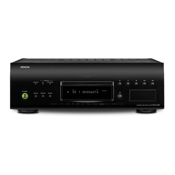
Denon DVD-A1UDCI Service Manual
Universal audio/video player
Hide thumbs
Also See for DVD-A1UDCI:
- Owner's manual (76 pages) ,
- Brochure & specs (13 pages) ,
- Specification sheet (2 pages)
Table of Contents
Advertisement
Ver. 2
Please refer to the
MODIFICATION NOTICE.
SERVICE MANUAL
MODEL
JP
E3
E2
EK
E2A E1C E1K EUT
DVD-A1UDCI
UNIVERSAL AUDIO/VIDEO PLAYER
For purposes of improvement, specifications and design are subject to change without notice.
●
Please use this service manual with referring to the operating instructions without fail.
●
Some illustrations using in this service manual are slightly different from the actual set.
●
e
D&M Holdings lnc.
X0403-2V02DM/DG0910
Copyright 2009 D&M Holdings Inc. All rights reserved.
WARNING: Violators will be prosecuted to the maximum extent possible.
Advertisement
Table of Contents

Related Manuals for Denon DVD-A1UDCI


Summary of Contents for Denon DVD-A1UDCI
- Page 1 MODIFICATION NOTICE. SERVICE MANUAL MODEL E2A E1C E1K EUT DVD-A1UDCI UNIVERSAL AUDIO/VIDEO PLAYER For purposes of improvement, specifications and design are subject to change without notice. ● Please use this service manual with referring to the operating instructions without fail.
-
Page 2: Safety Precautions
Care is also taken with the positions of the wores omsode amd clamps or other dangerous situations. are used to keep wires away from heating and high voltage parts, so be sure to set everything back as it was originally. DVD-A1UDCI... - Page 3 DIMENSION DVD-A1UDCI...
- Page 4 If wire bundles are untied or moved to perform adjustment or parts replacement etc.,be sure to rearrange them neatly as they were originally bundled or placed afterward. Otherwise, incorrect arrangement can be a cause of noise generation. Wire arrangement viewed from the top Front Panel side Back Panel side DVD-A1UDCI...
- Page 5 • Photographs for which no direction is indicated were taken from above the product. Direction of photograph: B The viewpoint of each photograph (Photografy direction) Front side [View from above] Direction of photograph: C Direction of photograph: D Direction of photograph: A DVD-A1UDCI...
-
Page 6: Front Panel Assy
Please refer to "EXPLODED VIEW" for the disassembly method of each P.W.B included in FRONT PANEL ASSY. 2. VIDEO/MAIN UNIT SUB ASSY Proceeding : TOP COVER → SIDE COVER (L) SUB ASSY → VIDEO/MAIN UNIT SUB ASSY (1) Remove the screws. Direction of photograph: A DVD-A1UDCI... -
Page 7: Video Unit
CX051 CY151 CX031 Direction of photograph: B FFC Cable MAIN UNIT FFC Cable CX044 (3) Cut the wire clamp band. Remove the screws, then remove “VIDEO/MAIN UNIT SUB ASSY". Refer to the diagram next page for instructions on removing. DVD-A1UDCI... - Page 8 ② Lift “VIDEO/MAIN SUB ASSY” in the direction of the arrow. ③ Draw out in the direction of the arrow. ② ③ R/P Side Please refer to "EXPLODED VIEW" for the disassembly method of each P.W.B included in VIDEO/MAIN UNIT SUB ASSY. DVD-A1UDCI...
- Page 9 : TOP COVER → SIDE COVER (L) SUB ASSY VIDEO/MAIN UNIT SUB ASSY DIGITAL CHASSIS SUB ASSY → → (1) Remove the screws. Direction of photograph: A DIGITAL CHASSIS SUB ASSY (2) Disconnect the connector wire. DIGITAL CHASSIS SUB ASSY CY033 DVD-A1UDCI...
-
Page 10: Power Unit
→ VIDEO/MAIN UNIT SUB ASSY → DIGITAL CHASSIS SUB ASSY → POWER UNIT (1) Cut the wire clamp band, then disconnect the connector wires. CX023 CX021 POWER UNIT Cord holder : Loose CX032 CY062 (2) Remove the screws. POWER UNIT DVD-A1UDCI... - Page 11 6. MIX AUDIO UNIT Proceeding : TOP COVER → SIDE COVER (R) SUB ASSY → MIX AUDIO UNIT (1) Remove the screws. Direction of photograph: A (2) Disconnect the connector board. Direction of photograph: C Board to board DVD-A1UDCI...
- Page 12 MIX AUDIO UNIT 7. 6ch AUDIO UNIT Proceeding : TOP COVER → SIDE COVER (R) SUB ASSY → MIX AUDIO UNIT → 6ch AUDIO UNIT (1) Remove the screws. Direction of photograph: A (2) Remove the screws. 6ch AUDIO UNIT DVD-A1UDCI...
-
Page 13: Power Trans
SIDE COVER (R) SUB ASSY → POWER TRANS (1) Disconnect the connector wire. Cord holder : Loose CX023 Acetate Tape (NITTOU No.156A) Direction of photograph: A Cord holder : Loose (2) Disconnect the connector wire, remove the screws. CX801 DVD-A1UDCI... - Page 14 (2) Remove the screws( ★ mark), then lift the clamp cover to unhook the hooks. (3) Remove the Clamp cover in the direction of the arrow, then remove the disc inside. Be careful not to scratch the disc when removing the Clamp cover. BLIND SHEET Hook clamp cover DVD-A1UDCI...
- Page 15 Laser drive current (Iop) check HF wave form check (Refer to WAVE FORMS) Current value of the BD, DVD or CD IOP is ± 12[mA] or more the initial value. FE Main P.W.B. and BD Mechanism Unit Assy replacing DVD-A1UDCI...
- Page 16 When “TC1”, “TC2” or “TC3” is selected with the 8 or 9 button, "mmmmmm" is displayed as “0” so you can check. FL Display (The display part of 13 digits) (Y=1 : CD, 2 : DVD , 3 : BD, mmmmmm : Time(Fractions of hours are counted up one hour on the display.) DVD-A1UDCI...
-
Page 17: Initial Setting Mode
(4) Each time the POP UP MENU button or Cursor buttons(d or f) on the remote control unit is pressed, µcom firm is displayed one after another. Ex (FL Display).: [Sys Ver000103, Sys Day090219, Sys GEN100000………H/W Ver000000, S/N***************] Ex (OSD).: DVD-A1UDCI... -
Page 18: Tray Lock Mode
(1) Pressing the PURE DIRECT 5 and SOURCE buttons for simultaneously. (2) “Lock-On” is displayed on the FL tube, and operations with the remote control and the REMOTE CONTROL input ter- minal on the back of the DVD-A1UDCI are disabled. 【Cancel】... -
Page 19: Entering The Test Mode
When the 8 button is pressed, the display switches in the opposite order fromq above, starting from the current position (for example, if currently at “TA”, it switches as follows: “T2, T3, T7, TC, TE, TG, TH, TI, T2 …”). DVD-A1UDCI... - Page 20 (10th place), the position moves to the uppermost position Use the 8 or 9 button to change the display at the address specification position. When the 2 button is pressed, the layer above the current layer is displayed. See "5.4 Stopping the mode" (page 23). DVD-A1UDCI...
- Page 21 If the 1 button is pressed while "TC4" is displayed, the accumulated laser on time of CD, DVD and BD is cleared. FL Display (The display part of 13 digits) When “TC1”, “TC2” or “TC3” is selected with the 8 or 9 button, "mmmmmm" is displayed as “0” so you can check. DVD-A1UDCI...
- Page 22 A confirmation message is displayed. Press the PLAY button to set, canceling the test mode. FL Display (The display part of 13 digits) When the 2 button is pressed, the layer above the current layer is displayed. See "5.4 Stopping the mode" (page 23). DVD-A1UDCI...
- Page 23 0x000000~0x000FFF HCSC BUF_ID_MPU_RSV6 0x000000~0x7DDFFF Reserved BUF_ID_MPU_RSV7 0x000000~0x3DFEFF Reserved BUF_ID_MPU_INT 0x000000~0x00003F BUF_ID_IRAM 0x000000~0x003FFF IRAM(internal SRAM) BUF_ID_DSP 0x000000~0x001FFF DSP Register BUF_ID_AFE 0x000000~0x0000FF AFE Register BUF_ID_SVO_ALL 0x000000~0x001FFF SVO REG ABS ACCESS BUF_ID_SVO_REG 0x000000~0x0007FF SVERVO REG BUF_ID_SVO_SVRAM 0x000000~0x0005FF SVRAM T57A BUF_ID_SVO_CRAM0 0x000000~0x0001FF CRAM0 DVD-A1UDCI...
- Page 24 The inner BIS error uncorrectable It is invalid. It is invalid. When this is selected for DVD 2-layer, it shifts to YY=85. circumference of signed number When this is selected for DVD 1-layer or 2-layer CD, it shifts to YY=73. DVD-A1UDCI...
- Page 25 PU# (16Byte) (Matched to TG pickup number display) A (A000 to A161 displayed in 2-digit units) Reserve (708Byte) B (B1 to B3 displayed in 4-digit units) Reserve (11Byte) Reserve (1Byte) D (D1 to D3 displayed in 4-digit units) Reserve (12Byte) DVD-A1UDCI...
- Page 26 HyBrid Disc current layer Current layer code BD-ROM DL 0x0014 SACD layer 0x0000 BD-Hybrid 0x0015 CD layer 0x0001 SACD-Hybrid 0x0016 DVD layer 0x0002 SACD DL 0x0017 BD layer 0x0003 SACD SL 0x0018 Other Reserved DVD-Hybrid 0v0019 Unknown 0xFFFF Other Reserved DVD-A1UDCI...
-
Page 27: Version Upgrade Procedure Of Firmware
Once updating starts, normal operations on the DVD-A1UD cannot be performed until updating is completed. Also, set- ting items of the GUI menu of DVD-A1UD or setting items of the image adjustment may be initialized. Make a note of the settings before updating, and set them again after updating. DVD-A1UDCI... - Page 28 2.1. Installation of application for IP ROM update Prepare a computer connected to the Internet. (1) From the SDI's DVD-A1UD or DVD-A1UDCI screen, download the following application software: • Soft : silicon developer toolkit 2.2. Preparations (proceeding to connections and the product mode) (1) Connect the set and computer using an RS-232C cable (straight type).
- Page 29 Check the selected file in the "Image File Path window" window, then click the "Update Firmware" button to begin updating. (4) During update, the update status is indicated " Burning flash, please wait...". (Approximately 9 minutes are required for updating to be completed.) DVD-A1UDCI...
-
Page 30: Version Check
•When the firmware is updated, the DVD-A1UD's settings and picture adjustments may be reset. Make a note of the set- tings before updating, and set them again after updating. •Do not unplug the RS-232C cable or set the power to standby during updating. •Normal operations are not possible during updating. DVD-A1UDCI... -
Page 31: Troubleshooting
[IC301](DAC for SBR/SBL) 3,5,18,19,42pin(WCK=16/8/4fs, BCK=512/256/128fs, DATA,MCK=512/256/128fs) O.K. Check DAC output Check Soldering 8U-210016-1(MIX UNIT) [IC101][IC102] [IC101][IC102]:output 6,8,9pin(control line) 8U-210016-2(SURROUND UNIT) [IC301][IC302][IC303] [IC301][IC302][IC303]:output 6,8,9pin(control line) Check Power Supply Voltage [CX141]:8U-210016-1 N.G. 1,2pin:about+12V/5,6pin:about+5V, 9,10pin:about-12V/14pin:about+3.3V, [CX142]:8U-210016-1 1,2pin:about+12V/5,6pin:about+5V, 9,10pin:about-12V/14pin:about+3.3V, [CX252]:8U-210016-1 4,5pin:about+5V/6pin:about+3.3V, [CX253]:8U-210016-2 4,5pin:about+5V O.K. DVD-A1UDCI... - Page 32 Check OUTPUT terminal Check Soldering 8U-210016-1(MIX UNIT) MUTE circuit:MUTE TR Check output signal from OUTPUT terminal 8U-210016-1(MIX UNIT) (Each channels) 8U-210016-2(SURROUND UNIT) Check output signal from OUTPUT terminal (Each channels) N.G. 8U-210016-2(SURROUND UNIT) TR-BASE terminal:about-12V (at MUTE off) O.K. DVD-A1UDCI...
-
Page 33: The Power Cannot Be Turned On
Check +24V output • [T101] (SW_TRANS) • Voltage Check N.G. • [IC108] (PC123-Y-22) 24V DC (switched) Voltage is O.K.? • [ZD102] (UDZS8.2B) [C160] L102 side output • [ZD103] (TL431ACLP) • [D111] (FME-210B) • [D104] (SJPX-F2) and Other Circuits O.K. DVD-A1UDCI... - Page 34 5V DC (switched) Voltage is O.K.? • [TR105,TR106] (TPCA8012-H) [CY051] 2pin output and Other Circuits O.K. Check Parts and Soldering. • [IC104] (MAX8577UEB) • [TR105,TR106] (TPCA8012-H) N.G. Is the rear side fan turning? 8U-310001 • [IC853] (R5F364VDNFB) and Other Circuits O.K. DVD-A1UDCI...
- Page 35 3.3V DC (switched) Voltage is O.K.? • FFC CABLE [CX191] 15pin output and Other Circuits O.K. Check Parts and Soldering. • [IC401] (PT6302-SSOP) • [FL401] (FL-TUBE(15-BT-114GNK)) • [CX161] (16P-TUCP-SOCKET) • [CX191] (19P-TUCP-SOCKET) • FFC cable and Other Circuits O.K. DVD-A1UDCI...
- Page 36 O.K. Check Video signals from MPEG Decoder Check Soldering. N.G. [CY801] and Circumference O.K. Check Audio Data and Clock Signals to DAC Check Soldering. N.G. [CY252][CY253] and Circumference Continue to the check process of Video or Analog Audio Unit DVD-A1UDCI...
- Page 37 [JK301] and Circumference O.K. Check Soldering. [IC200] and Circumference 4.3. No SD Card Operation Check SDDAT0-3, SDCLK, SDCD, SD-P_SENS Check Soldering. N.G. and SD_VDD33 [CX403] and Circumference [CX403] 25-40pin O.K. Check Soldering. 8U-210048-5 (SD UNIT) [CX182] [CX409] 8U-210048-2 (DISPLAY UNIT) [CY403] DVD-A1UDCI...
- Page 38 Unit (8U-310002) [CX801] • 3pin: PXD_CLK, 74.176MHz/74.25MHz(BD), N.G. Continue to the check process of PXD_HS, PXD_DE, PXD_VS 8U-310001(Main Unit) PXD_Y[11:4], PXD_CbCr[11:4] • 50pin: SDPX_CLK, 27MHz(DVD) SDPX_HS, SDPX_VS SDPX_S[7:0] O.K. Continue to the check process of each Video ter- minal DVD-A1UDCI...
- Page 39 O/3.3V, 100 ∼ 400kHz O.K. Check Digital Video signal output for Check Soldering. [IC601](ABT2010) • [X601] and Circumference N.G. • [R631] • ABTO_CLK: 27MHz, 74.176MHz, 74.25MHz • [R632][R633][R634] • ABTO_VS, ABTI_HS, ABTI_DE • [R635-644][R645-655] • ABTO_Y[11:2], ABTI_CbCr[11:2] O.K. Replace 8U-310002(Video Unit) DVD-A1UDCI...
- Page 40 O/3.3V, 100 ∼ 400kHz O.K. Check Digital Video signal output for Check Soldering. [IC601](ABT2010) • [X601] and Circumference N.G. • [R631] • ABTO_CLK: 27MHz, 74.176MHz, 74.25MHz • ABTO_VS, ABTI_HS, ABTI_DE • [R632][R633][R634] • [R635-644][R645-655] • ABTO_Y[11:2], ABTI_CbCr[11:2] O.K. Replace 8U-310002(Video Unit) DVD-A1UDCI...
- Page 41 DVD-A1UD and the TV.) Check Soldering. N.G. • [IC502](SiI9134), [JK601](HDMI Connector) • [IC502] and Circumference • TX-CLK +/-:[JK601] 10, 12pin • [JK605] • TX0 +/- :[JK601] 7, 9pin • TX1 +/- :[JK601] 4, 6pin • TX2 +/- :[JK601] 1, 3pin O.K. DVD-A1UDCI...
- Page 42 Check Soldering. N.G. • [IC504](SiI9134), [JK605](HDMI Connector) • [IC504] and Circumference • TX-CLK +/-:[JK605] 10, 12pin • [JK605] • TX0 +/- :[JK605] 7, 9pin • TX1 +/- :[JK605] 4, 6pin • TX2 +/- :[JK605] 1, 3pin O.K. Replace 8U-310002(Video Unit) DVD-A1UDCI...
- Page 43 8U-310010 (FE/SACD UNIT) • Check • [IC100][IC151][CX182] and Other Circuits Q1 Q2 O.K. Check signal of Thread system Check Parts and Soldering. N.G. MEASURING METHOD AND WAVEFORMS 8U-310010 (FE/SACD UNIT) • [IC100][IC151][CX182] and Other Circuits • Check Q3 ∼ O.K. DVD-A1UDCI...
- Page 44 --MEMO-- DVD-A1UDCI...
-
Page 45: Block Diagram
[EP3C40F484] 512Mbits DDR2 SDRAM IC108 COAX SYS u-com IC853 [R5F364VDNFB] COAX [K4T51163QG-HCE6] CLOCK GENERATE BLOCK FL DRV KEY CONT 1Gbits DDR2 SDRAM IC102 DENON Link [K4T1G084QG-HCE6] PLL1 CLK SEL DISPLAY PWB IR/REMO BE CONT POWER 1Gbits DDR2 SDRAM IC103 PLL2... - Page 46 --MEMO-- DVD-A1UDCI...
- Page 47 IDCK encrypted Capture / data D[35:0] ± Video VastLane Packetizer DE Gen / HSYNC Processing TMDS ± VSYNC Digital Logic ± Core Block ± control signals DCLK SPDIF MCLK Audio Data Capture audio data Logic SD[3:0] Block DL[3:0] DR[3:0] DVD-A1UDCI...
- Page 48 One-bit Audio Data Right 2 LVTTL Input One-bit Audio Data Left 3 LVTTL Input One-bit Audio Data Right 3 DCLK LVTTL Input One-bit Audio Clock Input MCLK LVTTL Input Audio Input Master Clock SPDIF LVTTL Input S/PDIF Audio Input DVD-A1UDCI...
- Page 49 R5F364VDNFB (8U-310001 : IC853) R5F364VDNFB Block Diagram DVD-A1UDCI...
- Page 50 R5F364VDNFB Pin Function DVD-A1UDCI...
- Page 51 DVD-A1UDCI...
- Page 52 Intput Buffer CK, CK Data Input Register LDMi Serial to parallel Bank Select 2Mx16 2Mx16 2Mx16 CK,CK 2Mx16 ADDR Column Decoder Latency & Burst Length Data Strobe Programming Register LCKE LRAS LCBR LCAS LWCBR CK,CK LDMi Timing Register CK,CK DVD-A1UDCI...
- Page 53 This pin is recommended to be left "No connection" on the device Reserved for future use *1 : The timing reference point for the differential clocking is the cross point of CK and CK. For any applications using the single ended clocking, apply V to CK pin. DVD-A1UDCI...
- Page 54 DAC 6 TEST DEINTERLEAVE DAC 6 ADAPTIVE FILTER PATTERN VIDEO CONTROL GENERATOR DATA POWER REFERENCE 16x/4x OVERSAMPLING VIDEO TIMING GENERATOR MANAGEMENT AND CABLE DAC PLL CONTROL DETECT RESET P_HSYNC P_VSYNC P_BLANK S_HSYNC S_VSYNC CLKIN (2) PV PGND EXT_LF COMP (2) DVD-A1UDCI...
- Page 55 ED = enhanced definition = 525p and 625p. LSB = least significant bit. In the ADV7344, setting the LSB to 0 sets the I C address to 0xD4. Setting it to 1 sets the I C address to 0xD6. DVD-A1UDCI...
- Page 56 DAC 6 TEST DEINTERLEAVE DAC 6 ADAPTIVE FILTER PATTERN VIDEO CONTROL DATA GENERATOR POWER REFERENCE 16x/4x OVERSAMPLING MANAGEMENT VIDEO TIMING GENERATOR AND CABLE DAC PLL CONTROL DETECT RESET P_HSYNC P_VSYNC P_BLANK S_HSYNC S_VSYNC CLKIN (2) PV PGND EXT_LF COMP (2) DVD-A1UDCI...
- Page 57 ED = enhanced definition = 525p and 625p. LSB = least significant bit. In the ADV7344, setting the LSB to 0 sets the I C address to 0xD4. Setting it to 1 sets the I C address to 0xD6. DVD-A1UDCI...
- Page 58 SHIFT REGISTER ADRAM 16 words x 2 bits DRIVER ADDRESS SELECTOR COMMAND DECODER WRITE READ ADDRESS ADDRESS COUNTER COUNTER PORT DRIVER CONTROL CIRCUIT DIGIT CONTROL GRID DRIVER DUTY CONTROL GR16 TIMING TIMING GENERATOR 1 GENERATOR 2 OSCO OSCILLATOR OSCI DVD-A1UDCI...
- Page 59 The serial data is shifted at the rising edge of CLKB. Serial data input pin Positive power supply P1 to P2 General purpose output pin 57 ~ 58 1 ~ 2 AD2 to AD1 Segment driver output pin 59 ~ 60 3 ~ 4 DVD-A1UDCI...
- Page 60 Sector Switches Erase Voltage Input/Output Generator Buffers RESET# State Control WP#/ACC BYTE# Command Register PGM Voltage Generator Data Chip Enable Latch Output Enable Logic Y-Decoder Y-Gating Detector Timer Cell Matrix X-Decoder **–A0 Note GL064N = A21, GL032N = A20. DVD-A1UDCI...
- Page 61 RESET# Hardware Reset Pin input RY/BY# Ready/Busy output BYTE# Selects 8-bit or 16-bit mode .0 volt-only single power supply (see Product Selector Guide for speed options and voltage supply tolerances) Output Buffer Power Device Ground Pin Not Connected Internally DVD-A1UDCI...
- Page 62 AK4399EQ (8U-210016 : IC101) AK4399EQ Block Diagram DVD-A1UDCI...
- Page 63 AK4399EQ Pin Function DVD-A1UDCI...
- Page 64 DVD-A1UDCI...
- Page 65 P-port input/output. Push-pull design structure. P-port input/output. Push-pull design structure. Address input. Connect directly to V or ground. Serial clock bus. Connect to V through a pullup resistor. Serial data bus. Connect to V through a pullup resistor. Supply voltage DVD-A1UDCI...
- Page 66 Shutdown Input. With SD = 5V (HIN213E SD = 0V), the charge pump is disabled, the receiver outputs are in a high impedance state (except R4 and R5 of HIN213E) and the transmitters are shut off. No Connect. No connections are made to these leads. DVD-A1UDCI...
- Page 67 2. FL DISPLAY FL TUBE (15-BT-114GNK) (8U-210048 : FL401) DVD-A1UDCI...
- Page 68 --MEMO-- DVD-A1UDCI...
- Page 69 PRINTED WIRING BOARDS 8U-210016 ANALOG AUDIO P.W.B. UNIT(1/2) COMPONENT SIDE DVD-A1UDCI...
- Page 70 8U-210016 ANALOG AUDIO P.W.B. UNIT(2/2) FOIL SIDE DVD-A1UDCI...
- Page 71 8U-210048 POWER/DISPLAY P.W.B. UNIT(1/2) COMPONENT SIDE DVD-A1UDCI...
- Page 72 8U-210048 POWER/DISPLAY P.W.B. UNIT(2/2) FOIL SIDE DVD-A1UDCI...
- Page 73 8U-310001 MAIN P.W.B. UNIT(1/2) COMPONENT SIDE DVD-A1UDCI...
- Page 74 8U-310001 MAIN P.W.B. UNIT(2/2) FOIL SIDE DVD-A1UDCI...
- Page 75 8U-310002 VIDEO P.W.B. UNIT(1/2) COMPONENT SIDE DVD-A1UDCI...
- Page 76 8U-310002 VIDEO P.W.B. UNIT(2/2) FOIL SIDE DVD-A1UDCI...
- Page 77 8U-310010 FE/SACD P.W.B. UNIT FOIL SIDE COMPONENT SIDE DVD-A1UDCI...
- Page 78 1U-3791 FGCX P.W.B. UNIT 8U-210075A FE REG PWB UNIT ASSY COMPONENT SIDE FOIL SIDE FOIL SIDE COMPONENT SIDE FOIL SIDE COMPONENT SIDE FOIL SIDE DVD-A1UDCI...
-
Page 79: Note For Parts List
Indicates number of zeros after efective number. (0 or 1) (More than 2) 2-digit effective number. 2-digit effective number. ・ Units:pF ・ Units:pF ・ When the dielectric strength is indicated in AC,"AC" is included after the dieelectric strength value. DVD-A1UDCI... -
Page 80: Parts List Of P.w.b. Unit
TR350-355 00D2690119901 DTA124EKT96(TAPE) TR801-804 00D2730460905 KTC2875-B-RTK/P TR805 00D2690082902 DTC114EKT96 TR806 00D2690119901 DTA124EKT96(TAPE) D101,102 00D2760717903 1SS355 TE-17 D104 00D2760701003 S2L20U-4002P7.5 D106,107 00D2760701003 S2L20U-4002P7.5 D109 00D2760701003 S2L20U-4002P7.5 D111-116 00D2760723900 RB721Q-40 RESISTORS GROUP R111 119310006524S MMZ1608D241C R127 RS14B3A182JNBST(S) R129,130 RS14B3A182JNBST(S) R210,211 RS14B3A182JNBST(S) DVD-A1UDCI... - Page 81 C159 0.01UF,J,M,50V C166-169 CK73F1E104ZT +1608 C174-177 CK73F1E104ZT +1608 C178-181 0.01UF,J,M,50V C182-185 00MDF15471351 470PF,J,M,50V C186,187 0.0018UF,J,M,50V,D=9,N/IND(M) C192-195 0.01UF,J,M,50V C196,197 00MDF15222351 0.0022UF,J,M,50V C204-207 0.00022UF J M 50V C208-211 0.0018UF,J,M,50V,D=9,N/IND(M) C212,213 0.01UF,J,M,50V C214-216 CK73F1E104ZT +1608 C217-220 00D2543091901 CE04D1H220MBPT (RBD) C221 CK73F1E104ZT +1608 DVD-A1UDCI...
- Page 82 +1608 C333,334 CK73F1E104ZT +1608 C335-341 CC73CH1H101JT +1608 C342-344 00D2544583971 CE04W1H470MT(ROB) C345-350 CF73=1C104JT(ECHUB5)+3225 C351-353 00D2544583971 CE04W1H470MT(ROB) C354-359 00D2544693939 CE04W1H101MT(RF0) C362,363 CK73F1E104ZT +1608 C366,367 CK73F1E104ZT +1608 C370,371 CK73F1E104ZT +1608 C372-383 CF73=1C104JT(ECHUB5)+3225 C384-395 00D2544693939 CE04W1H101MT(RF0) C396 0.01UF,J,M,50V C411-422 CK73F1E104ZT +1608 C423-428 0.0018UF,J,M,50V,D=9,N/IND(M) DVD-A1UDCI...
- Page 83 CX801 3P VH CON.BASE CY141,142 14P CON.BASE TUC-P JK101,102 00D2051448004 3P CANNON CON.(AU)OUT JK103,104 643010023605S 1P PIN JACK(AU,shield) JK301-306 643010023605S 1P PIN JACK(AU,shield) W102 M3 SCREW TERMINAL 3X8 CPS(SW,W) ZNP IC801-804 00D1259002065 UL TUBE (L=15) 00D2544763018 CE04W1V471M(RFO) RUBBER SHEET DVD-A1UDCI...
- Page 84 D108,109 00D2760750902 RB521S-30TE61 +REF D110 203850008503S SJPX-F2 D111 204050011708S FME-210B D112-119 00D2760750902 RB521S-30TE61 +REF D120 00D2760717903 1SS355 TE-17 D123 00D2760717903 1SS355 TE-17 D124,125 203850012502S SJPB-L4 D131 00D2760717903 1SS355 TE-17 D133,134 203850008503S SJPX-F2 D135 00D2760717903 1SS355 TE-17 D137 203850012502S SJPB-L4 DVD-A1UDCI...
- Page 85 C107,108 00D2538035710 CK45E2EAC222MC(KY) C109 00D2544708701 CE04W1V471MC J20(KY) C110 00D2538035710 CK45E2EAC222MC(KY) C111,112 00D2568039029 CF99--2EAC334K(LEMX) C113 00D2538035710 CK45E2EAC222MC(KY) C114 00D2538029713 CK45F2EAC471KC(KX) C115,116 00D2538035710 CK45E2EAC222MC(KY) C117 134010168219S CE68W2D471M Q30(KMM) C118 00D2538026703 CK45E2EAC472MC C119 00D2544708701 CE04W1V471MC J20(KY) C120 132050024205S CK45B3D102KC(DEHR) C122 CK73B1A224KT +1608 DVD-A1UDCI...
- Page 86 C182 CK73R1H104KT (1608) C184 CC73CH1E681JT +1608 C185 CK73B1E104KT +1608 C186 CK73X7R1H225KT(GRM_3216) C187 CK73R1H103KT (1608) C188 00D2571020915 CK73B1H225KT C189-191 CK73B1H103KT (1608) +1608 C192,193 00D2544708701 CE04W1V471MC J20(KY) C194,195 CK73X7R1H225KT(GRM_3216) C197 CK73B1H102KT +1608 C199 CK73B1H102KT +1608 C200 00MDK2647601Y GRM32EB31C476KE15L C201 CK73F1E104ZT +1608 DVD-A1UDCI...
- Page 87 +1608 C270 CK73B1H102KT +1608 C271 CK73B1H222KT +1608 C272,273 CK73B1H102KT +1608 C274 GRM32EB31C476KE15L C275 CK73B1H103KT (1608) +1608 C276 CK73B1H102KT +1608 C277,278 00MDK2647601Y GRM32EB31C476KE15L C279 CK73B1H102KT +1608 C280 CK73B1H103KT (1608) +1608 C281 CK73B1H102KT +1608 C282,283 CK73B1H103KT (1608) +1608 C284 CK73B1E104KT +1608 DVD-A1UDCI...
- Page 88 CK73B1H103KT (1608) +1608 C450 CK73B1H102KT +1608 C451 CK73B1H103KT (1608) +1608 C453-456 00D2544722907 CE04W1H0R1MT(GR) C457 00D2544718937 CE04W1C470MT(GR) C458 CK73B1H103KT (1608) +1608 C459 00D2544722949 CE04W1H010MT(GR) C460 00D2544718937 CE04W1C470MT(GR) C461 CK73F1E104ZT +1608 C462 CC73CH1H101JT +1608 C463,464 CK73B1H103KT (1608) +1608 C466 CK73B1H103KT (1608) +1608 DVD-A1UDCI...
- Page 89 CY182 00D2051329013 18P FFC BASE(9610SB) CY191 19P CON.BASE TUC-P CY403 00D2051465906 40P-FFC-BASE(FH12) F101 00D2061099045 FUSE(02153.15MXP/250V) FB401-405 00D2350147909 E.FIL(BLM21PG221SN1)+2125 FF101 FUSE CLIP(TAPE) FH101 FUSE CLIP(TAPE) JK401,402 00D2048260004 MINI JACK JK403 00D2051305008 9P D-SUB CONNECTOR L101 00D2390038023 L.FILTER(HR28R-E332) L102 111010010249S INDUCTOR(PC13-3R9N) DVD-A1UDCI...
- Page 90 GND TERMINAL FOR PCB W105 GND TERMINAL FOR PCB W107-112 GND TERMINAL FOR PCB W301,302 GND TERMINAL FOR PCB W405 M3 SCREW TERMINAL W406 M3 SCREW TERMINAL W407,408 M3 SCREW TERMINAL W409,410 M3 SCREW TERMINAL 3X8 CPS(SW,W) ZNP RUBBER SHEET DVD-A1UDCI...
- Page 91 BU2365FV-E2 IC719 SM5158AM-G-E2 IC851 BD4730G-TR IC852 S-24CS08AFJ-TB IC853 SYSTEM ROM SUB ASSY (R5F364VDNFB) IC854,855 SN74LVC157APW-EL2 TR301,302 KRC102S-RTK/P (10K-10K) TR451 KRC102S-RTK/P (10K-10K) TR452,453 KRA102S-RTK/P (10K-10K) TR454 KRC102S-RTK/P (10K-10K) TR551 KRC102S-RTK/P (10K-10K) TR552 KRA102S-RTK/P (10K-10K) TR651 2SC2412K_T146R TR851 DTC144EKT96 TR852 2SB1132T100Q DVD-A1UDCI...
- Page 92 +1005 C134-141 CK73B1A104KT +1005 C150-165 CK73B1A104KT +1005 C166 CS77B0J470MT(NOJ) C167-170 CK73B1A104KT +1005 C171 CS77B0J470MT(NOJ) C172-174 CK73B1A104KT +1005 C175-186 CK73F1C104ZT +1005 C187-194 CK73B1A104KT +1005 C200-211 CK73B1A104KT +1005 C212 CS77B0J470MT(NOJ) C213 CK73B1A104KT +1005 C214 CS77B0J470MT(NOJ) C215-226 CK73F1C104ZT +1005 C227-236 CK73B1A104KT +1005 DVD-A1UDCI...
- Page 93 CK73B1A106KT +2125 C752 CK73F1C104ZT +1005 C753 CK73F1H103ZT +1005 C757 CC73CH1H100DT +1005 C758 CK73B1H222KT +1005 C759 CC73CH1H100DT +1005 C760-763 CS77B0J220MT(NOJ) C764-768 CK73B1A104KT +1005 C769 CS77B0J220MT(NOJ) C802 CK73F1C104ZT +1005 C803 CE67C0J220MT (RV2) +REF C805 CK73F1C104ZT +1005 C806 CK73D0J226MT(3216) C807 CK73F1C104ZT +1005 DVD-A1UDCI...
- Page 94 C950 CK73D0J226MT(3216) C951 CK73B0J475KT +1608 C952 CK73F1E104ZT +1608 C953 CK73D0J226MT(3216) C954 CK73F1H103ZT +1608 C955,956 CK73B1H102KT +1608 C957 CK73B1H103KT (1608) +1608 C958 CK73B1E104KT +1608 C959 CK73D0J226MT(3216) C961 CK73B1E104KT +1608 C962 CK73B0J226MT C965 CK73B0J226MT C967 CK73B0J226MT C968 CK73B1E104KT +1608 C971,972 CK73B0J226MT DVD-A1UDCI...
- Page 95 CK73B0J475KT +1608 CC438,439 CC73CH1H7R0DT +1005 CC501-508 CC73CH1H101JT +1005 CC509-516 CK73B1H102KT +1005 CC517-524 CK73B1A104KT +1005 CC525 CS77B1A100MT(NOJ) CC527,528 CK73B1A104KT +1005 CC530,531 CK73B1A104KT +1005 CC532 CK73B0J475KT +1608 CC534 CK73B1A104KT +1005 CC535 CK73B0J475KT +1608 CC538,539 CC73CH1H7R0DT +1005 CC601 CK73D0J226MT(3216) CC602,603 CK73F1C104ZT +1005 DVD-A1UDCI...
- Page 96 +1608 FB916 E.FIL(BLM21PG221SN1)+2125 JK301 00D2051333009 8P MODULAR JK651 643010023605S 1P PIN JACK(AU,shield) JK652 00D2051222000 RJ-45 JACK(GND) W651,652 M3 SCREW TERMINAL X300 FCX-03(25MHZ) X451 FCX-03(20.815MHz) X551 FCX-03(20.815MHz) X651 FCX-03(24.576MHz) X705 FCX-03(27.000MHz) 15ppm X851 TFX-02(32.768kHz) X852 FCX-03(20.000MHz) 20ppm 2P 80mm ZM DVD-A1UDCI...
- Page 97 +REF D201,202 RB521S-30TE61 +REF D501-503 KDS160-RTK/P D504-508 ESD PROTECTOR(6802) D509-516 AVRL161A1R1NTB D517-521 ESD PROTECTOR(6802) D522-529 AVRL161A1R1NTB D701 RB521S-30TE61 +REF D801-803 KDS160-RTK/P ZD501,502 UDZS5.1B-TE17 RESISTORS GROUP R356,357 RM73B--103FT +1608 R359,360 RM73B--103FT +1608 R725,726 RM73B--102FT +1608 R732,733 RM73B--102FT +1608 RA201-240 MNR04=330(1005X4) DVD-A1UDCI...
- Page 98 RM73B--162FT RR336 RM73B--750FT RR337 RM73B--162FT RR338 RM73B--331FT RR359,360 RM73B--750FT RR361 RM73B--162FT RR362 RM73B--331FT RR383,384 RM73B--750FT RR611 RM73B--222DT(1608) RR613 RM73B--510DT(1608) RR647 RM73B--331DT(1608) RR648 RM73B--272DT(1608) RR649 RM73B--102FT +1608 RR652-654 RM73B--102FT +1608 RR814 RM73B--511DT(1608) RR850 RM73B--750DT(1608) RR852 RM73B--750DT(1608) RR857 RM73B--750DT(1608) RR859 RM73B--750DT(1608) DVD-A1UDCI...
- Page 99 RM73B--221JT +1608 RS826,827 RM73B--0R0KT+1005 RS828,829 RM73B--331JT RS830-839 RM73B--0R0KT +1608 RS840,841 RM73B--331JT RS842 RM73B--0R0KT +1608 RS843 RM73B--301DT(1608) RS845 RM73B--330JT +1608 RS846 RM73B--102JT +1608 RS847 RM73B--0R0KT +1608 RS848 RM73B--301DT(1608) RS850 RM73B--330JT +1608 RS851 RM73B--102JT +1608 RS853 RM73B--0R0KT +1608 RS855 RM73B--0R0KT +1608 DVD-A1UDCI...
- Page 100 C192 CS77B1A100MT(NOJ) C205 CK73B1E103KT(1005) C206 CS77B1A100MT(NOJ) C207 CK73B1A104KT +1005 C208 CK73B1E103KT(1005) C209,210 CC73CH1H470JT C217 CK73B1E103KT(1005) C218 CC73CH1H101JT +1005 C222-224 CK73B1A106KT +2125 C225-227 CK73B1E103KT(1005) C228 CK73B1A106KT +2125 C229,230 CK73B1E103KT(1005) C231 CK73B1A106KT +2125 C232-284 CK73B1E103KT(1005) C285,286 CK73D0J226MT(3216) C287-297 CK73B1E103KT(1005) C298 CK73D0J226MT(3216) DVD-A1UDCI...
- Page 101 CK73B1H102KT +1005 C610 CK73B1A104KT +1005 C611 CK73B1H102KT +1005 C612,613 CK73B1A104KT +1005 C614 CK73B1A106KT +2125 C615 CK73B1A104KT +1005 C616 CK73B1H102KT +1005 C617 CK73B1A104KT +1005 C618 CK73B1H102KT +1005 C619 CK73B1A106KT +2125 C620 CK73D0J226MT(3216) C621-642 CK73B1A104KT +1005 C643 CK73B1E103KT(1005) C644 CK73B1H102KT +1005 DVD-A1UDCI...
- Page 102 C844 CK73B1A104KT +1005 C845-847 CK73B1E103KT(1005) C848 CK73B1A104KT +1005 C849 CK73B1E103KT(1005) C850 CK73B1H123KT +1608 C851 CK73B1A154KT +1608 C852 CK73B1A104KT +1005 C853 CK73B1H102KT +1005 C854,855 CK73B1A106KT +2125 C856,857 CK73B1H102KT +1005 C858 CK73B1A104KT +1005 C859 CK73B1E103KT(1005) C860 CK73B1A106KT +2125 C861 CK73B1A104KT +1005 DVD-A1UDCI...
- Page 103 CK73B1A104KT +1005 C930 CK73B1H102KT +1005 C931 CK73B1A106KT +2125 C932 CK73B1A154KT +1608 C933 CK73B1H123KT +1608 C934 CK73B1A106KT +2125 C935 CK73B1A104KT +1005 C936 CK73B1H102KT +1005 C937 CK73B1A154KT +1608 CC127 CK73B1A104KT +1005 CC129,130 CK73B0J475KT(P) +1608 CC131-138 CK73B1A104KT +1005 CC139-146 CK73B1H102KT +1005 CC201-209 CK73B1E103KT(1005) DVD-A1UDCI...
- Page 104 CK73B1H102KT +1005 CC410 CK73B1E103KT(1005) CC411 CK73B1A104KT +1005 CC412 CK73B1A106KT +2125 CC501,502 CK73B0J475KT(P) +1608 CC503-506 CK73B1H102KT +1005 CC507-509 CK73B1A104KT +1005 CC510-512 CK73B1H102KT +1005 CC513 CK73B1A104KT +1005 CC514,515 CK73B1H102KT +1005 CC516,517 CK73B1A104KT +1005 CC518 CK73B1H102KT +1005 CC519-521 CK73B1A104KT +1005 CC522 CK73B1H102KT +1005 DVD-A1UDCI...
- Page 105 +1608 FB202-207 MPZ1608S221A FB208 FBMJ1608HS280NT +1608 FB501 FBMJ1608HS280NT +1608 FB502-517 MPZ1608S221A FB601-608 MPZ1608S221A FB701 MPZ1608S221A FB702 FBMJ1608HS280NT +1608 FB703 MPZ1608S221A FB802-814 FBMJ1608HS280NT +1608 FB888-890 FBMJ1608HS280NT +1608 JK601 644010062702S HDMI CONNECTOR JK605 644010062702S HDMI CONNECTOR JK901-904 643010023605S 1P PIN JACK(AU,shield) DVD-A1UDCI...
- Page 106 00D2051395005 1P S-TERMINAL-LF L803 INDUCTOR(FLC32C220K)+3216 L806 INDUCTOR(FLC32C220K)+3216 L901 INDUCTOR(FLC32C220K)+3216 RL501,502 RELAY(UB2-5NUN-L1) W102-104 M3 SCREW TERMINAL X201 FCXO-05(66.666MHz) X601 FCXO-05 (30.00MHz) X801 FCXO-05 (27.00MHz) 1P CONTACT ASSY 140&165mm HEAT SHEET (GP1-2.0) HEAT SINK(PUE-56) HEAT SINK BRACKET 3X6 CFS-B CUPPER TAPE(W=15) DVD-A1UDCI...
- Page 107 D901,902 1SS355 TE-17 D903-905 1SR154-400TE25 +REF D906-910 1SS355 TE-17 RESISTORS GROUP R137 RS14B3A010JNBST(S) R159 RM73B--123FT +1608 R253,254 RM73B--103DT_1005 R255 RM73B--332DT(1608) R273,274 RM73B--103DT_1005 R320 RM73B--123FT +1608 R322 RM73B--224DT(1608) RR130 RS14B3A010JNBST(S) RR139-142 RM73B--103DT_1005 RR905-907 RM73B--102FT +1608 RR917 RM73B2B0R0KT +3216 RA401,402 MNR14=220JE0AB DVD-A1UDCI...
- Page 108 C165 CC73CH1H101JT +1005 C166 CK73B1A106KT +2125 C167-170 CK73F1C104ZT +1005 C171,172 CK73F1H103ZT +1005 C173 CK73F1C104ZT +1005 C174 CE67C1C220MT (RV2) +REF C175-177 CK73F1C104ZT +1005 C178 CK73F1H103ZT +1005 C179 CK73F1C104ZT +1005 C180,181 CK73F1H103ZT +1005 C182 CK73B1E103KT(1005) C185-187 CK73F1H103ZT +1005 C188,189 CK73F1C104ZT +1005 DVD-A1UDCI...
- Page 109 +1005 C418 CK73F1C104ZT +1005 C423-426 CK73F1C104ZT +1005 C427 CE67C0J101MT (RV2) +REF C428-432 CK73F1C104ZT +1005 C433 CE67C0J101MT (RV2) +REF C434 CK73F1H103ZT +1005 C435 CK73F1C104ZT +1005 C501 CK73F1C104ZT +1005 C502 CC73CH1H102JT +1608 C503 CK73F1C104ZT +1005 C504 CC73CH1H102JT +1608 C505 CK73F1C104ZT +1005 DVD-A1UDCI...
- Page 110 C914 CE67C0J220MT (RV2) +REF C915 CK73F1C104ZT +1005 C916 CK73B1H103KT (1608) +1608 C917 CK73F1H103ZT +1005 C918 CK73B1A106KT +2125 C919 CK73F1C104ZT +1005 C920 CK73F1H103ZT +1005 C921 CK73B1A106KT +2125 C922 CC73CH1H471JT +1608 C923,924 CK73F1C104ZT +1005 C925,926 CE67C0J220MT (RV2) +REF C927,928 CK73B1A106KT +2125 DVD-A1UDCI...
- Page 111 +REF CX182 18P-FFC-BASE(9617S) CX402 40P-FFC-BASE(FH12) CX451,452 45P-FFC-BASE(9637SA) FB101-105 FBMJ1608HS280NT +1608 FB106,107 RM73B--0R0KT +1608 FB301,302 RM73B--0R0KT +1608 FB901,902 FBMJ1608HS280NT +1608 FB904-908 FBMJ1608HS280NT +1608 FB910,911 FBMJ1608HS280NT +1608 FB912,913 MMZ1608D241C FB914-919 FBMJ1608HS280NT +1608 FB920-931 RM73B--0R0KT +1608 FB932 FBMJ1608HS280NT +1608 FB933-936 RM73B--0R0KT +1608 DVD-A1UDCI...
- Page 112 Part No. Part Name Remarks Q'ty SEMICONDUCTORS GROUP LD101,102 00D2690220007 GP1S094HCZ(JP) CAPACITORS GROUP C101-105 CK73B1E104KT +1608 OTHERS PARTS GROUP CX031 3P CONN.BASE(KR-PH) CX032 3P CONN.BASE(KR-PH) CX033 3P CONNE.BASE(BLK) CX061 6P CONN.BASE(KR-PH) CX071 7P CONN.BASE(KR-PH) CY051 5P CONN.BASE(KR-PH) S101 00D2121206008 SPVF130100 DVD-A1UDCI...
-
Page 113: Wiring Diagram
39 40P-FFC UL20706 CY404 CY253 Inter-Face CW404 8U-310001 CY142 CY801 Main 80P-BtoB CX082 BE/ Digital Audio/ Sys u-Com CX801 CX404 CX031 CX051 14P-TUC CX142 8U-310002 240mm Video CX253 8U-210016-2 Analog Audio 2 CY082 8U-210048-3 RS-232C FAN 1 FAN 2 DVD-A1UDCI... -
Page 114: Exploded View
EXPLODED VIEW WARNING: 67-1 Parts marked with this symbol have critical characteristics. Use ONLY replacement parts recommended by the manufacturer. 67-2 24 209 44-1 44-2 44-3 DVD-A1UDCI... -
Page 115: Parts List Of Exploded View
FAN(3110RL-04W-S29-C04_80X80X25) FAN SPACER FAN BRACKET 00D2033996008 AC INLET (2P) 00MFC50250020 TFCK-25-15-12 ★ 25 00D3420032040 FERRITE CLAMP(RFC-8) ★ 26 FFC HOLDER(C) 00D4611247032 RUBBER SHEET PUR FOAM PUR FOAM PUR FOAM PUR FOAM LASER LABEL(BD) FFC HOLDER DIGITAL CHASSIS 449010013004D FAN(3110RL-04W-S29-C04_80X80X25) DVD-A1UDCI... - Page 116 Q'ty 00D4490033052 LOCKING CARD SPACER 00D3420032024 FERRITE CLAMP(RFC-9) ★ 39 00MFC50230010 TFCK-23-11-14 ★ 40 402310052205D FRONT PANEL(CIBKE3) 421410005001D DENON BADGE 00D1430952002 LENS 443510017300D INNER PANEL(BK) 44-1 SET UP KNOB BASE 3P 44-2 GEAR DAMPER STOPPER 44-3 SPRING STOPPER 416510028001D WINDOW...
- Page 117 CW182 ★ 306 2P 440mm VA CW021 ★ 307 4P 310mm VH-VH CW044 ★ 308 5P 320mm VH-VH CW051 ★ 309 15P 210mm PH-PH CW151 ★ 310 4P 310mm PH-PH CW041 ★ 311 6P 290mm VH-VH CW062 ★ 312 DVD-A1UDCI...
- Page 118 --MEMO-- DVD-A1UDCI...
- Page 119 EXPLODED VIEW OF SACD MECHANISM WARNING: Parts marked with this symbol have critical characteristics. Use ONLY replacement parts recommended by the manufacturer. DVD-A1UDCI...
- Page 120 MECHA BASE back Grease : EM30L CAM SPRING attachment area(0.9mg) Both ends side of boss contact area under MECA BASE-SLIDE CAM. (7.0mg each x 2) Grease : EM30L Only shaft area of gear axis (2.0mg each x 2) Greasing position DVD-A1UDCI...
- Page 121 DAMPER RING MOTOR BRACKET ASS'Y CAM HOLDER SW BRACKET REAR BRACKET ASS'Y 00D4630973105 CAM SPRING SWITCH SHEET 00D4630975006 SHAFT SPRING 00D4751179011 WASHER SLIDE SHAFT BD TRAVERSE UNIT 00D9KA2A762 LOADING MOTOR ASSY MOTOR PULLY LOADINGMOTOR BRACKET LOADING MOTOR 2.6 × 3CBS-B DVD-A1UDCI...
- Page 122 3P SHS CONN.CORD ★ 80 00D2038578007 5P SHS CONN.CORD ★ 81 00D2035396004 3P SHS CONN.CORD ★ 82 448010009002D SUS BRUSH 451310070007D ALUMINUM SHEET 00D4220681001 ROLLER SHAFT 451010041002D SHIELD GUIDE 445510069000D FPC COVER MECHA BRACKET 0RD4700009022 3 × 6CPS(SW.W)ZNP BOTTOM_SHEET DVD-A1UDCI...
-
Page 123: Packing View
PACKING VIEW ∼ ∼ DVD-A1UDCI... -
Page 124: Parts List Of Packing & Accessories
BATTERY(UM-3)ASSY 307010028003D RC-1111 ENVELOPE 541110186005D INST. MANUAL(DVD-A1UDCIBKE3) S/No. ~09999 541110186104D INST. MANUAL(DVD-A1UDCIBKE3) S/No. 10001~ BAR CODE LABEL ASSY 543110032104D S.S.LIST (EX) ★ 219 00DGEN0225 CONT.CARD(L)SUB ASSY ★ 220 00D5150944901 WARRANTY (HOME) ★ 221 541110384007D INST.SHEET(BD-LIVE)DVDA1UD-E3 S/No. ~09999 ★ 222 DVD-A1UDCI... -
Page 125: Measuring Method And Waveforms
IOP. When watching the HF waveform (ATEST), use the extending wire as short as possible. ※ It is better to use wires for extending between the probe and test points. ※ 1. MAIN UNIT : TEST POINT AND WAVEFORMS 8U-310010 FE/SACE UNIT : Component Side DVD-A1UDCI... - Page 126 Q6 SL2- BD LOADING → PLAY BD SEARCH (OUTER → INNER) Q3 SLED+ t FODN Q4 SLED- y FCS2+ Q5 SL1+ u FCS2- Q6 SL2- BD PLAY i TRD o TRK+ Q0 TRK- DVD-A1UDCI...
- Page 127 Q6 SL2- DVD LOADING → PLAY DVD SEARCH (OUTER → INNER) Q3 SLED+ t FODN Q4 SLED- y FCS2+ Q5 SL1+ u FCS2- Q6 SL2- DVD PLAY i TRD o TRK+ Q0 TRK- DVD-A1UDCI...
- Page 128 Q6 SL2- CD LOADING → PLAY CD SEARCH (OUTER → INNER) Q3 SLED+ t FODN Q4 SLED- y FCS2+ Q5 SL1+ u FCS2- Q6 SL2- CD PLAY i TRD o TRK+ Q0 TRK- DVD-A1UDCI...
- Page 129 ANALOG VIDEO OUTPUT SIGNAL Signal: Color Bar 100% DVD-A1UD Oscilloscope 75ohm Loard Analog Video 出力信号 測定 Signal: Color Bar 100% Composite DVD-A1UD Oscilloscope 75ohm Loard Composite S (Y/C) S (Y/C) Component (Y, Cb, Cr) 480/59.94i Component (Y, Cb, Cr) 480/59.94i DVD-A1UDCI...
-
Page 130: Note For Schematic Diagram
NOTICE: ALL RESISTANCE VALUES IN OHM. k=1,000 OHM M=1,000,000 OHM ALL CAPACITANCE VALUES IN MICRO FARAD. P=MICRO-MICRO FARAD EACH VOLTAGE AND CURRENT ARE MEASURED AT NO SIGNAL INPUT CONDITION. CIRCUIT AND PARTS ARE SUBJECT TO CHANGE WITHOUT PRIOR NOTICE. DVD-A1UDCI... - Page 131 Q0 e y o BD DATA OUTPUT SIGNAL LINE SACD/DVD/CD DATA OUTPUT SIGNAL LINE BD/SACD/DVD/CD DATA OUTPUT SIGNAL LINE SCHEMATIC DIAGRAMS (1/45) 8U-310010-1 FE/SACD UNIT (1/6) FE BLOCK DVD-A1UDCI...
- Page 132 SCHEMATIC DIAGRAMS (2/45) BD/SACD/DVD/CD PLAY DATA OUTPUT SIGNAL LINE 8U-310010-1 FE/SACD UNIT (2/6) BD/SACD/DVD/CD CONTROL DATA OUTPUT SIGNAL LINE SATA-ATAPI BLOCK DVD-A1UDCI...
- Page 133 SACD PLAY DATA OUTPUT SIGNAL LINE SCHEMATIC DIAGRAMS (3/45) 8U-310010-1 FE/SACD UNIT (3/6) SACD DECODE BLOCK DVD-A1UDCI...
- Page 134 SCHEMATIC DIAGRAMS (4/45) SACD PLAY DATA OUTPUT SIGNAL LINE 8U-310010-1 FE/SACD UNIT (4/6) VSTEM-ATAPI BLOCK SACD CONTROL DATA OUTPUT SIGNAL LINE DVD-A1UDCI...
- Page 135 BD/SACD/DVD/CD PLAY DATA OUTPUT SIGNAL LINE SCHEMATIC DIAGRAMS (5/45) BD/DVD/CD PLAY DATA OUTPUT SIGNAL LINE 8U-310010-1 FE/SACD UNIT (5/6) BD/SACD/DVD/CD CONTROL DATA OUTPUT SIGNAL LINE BUS SW BLOCK SACD PLAY DATA OUTPUT SIGNAL LINE DVD-A1UDCI SACD CONTROL DATA OUTPUT SIGNAL LINE...
- Page 136 +12V +3.3V +3.3V +1.5V +1.5V +1.8V +1.2V +3.3V +2.5V SCHEMATIC DIAGRAMS (6/45) 8U-310010-1 FE/SACD UNIT (6/6) POWER BLOCK DVD-A1UDCI...
- Page 137 SCHEMATIC DIAGRAMS (7/45) 1U-3791-1 Loading SENS UNIT DVD-A1UDCI...
- Page 138 SCHEMATIC DIAGRAMS (8/45) 1U-3791-2 Loading UNIT 1U-3791-3 Chacking UNIT DVD-A1UDCI...
- Page 139 SCHEMATIC DIAGRAMS (9/45) 8U-210075 FE REG UNIT DVD-A1UDCI...
- Page 140 SCHEMATIC DIAGRAMS (10/45) 8U-310001 MAIN UNIT(1/13) BE LSI BLOCK BD/DVD/CD PLAY A/V OUTPUT SIGNAL LINE BD/DVD/CD PLAY AUDIO OUTPUT SIGNAL LINE DVD-A1UDCI BD/DVD PLAY VIDEO OUTPUT SIGNAL LINE BD/DVD/CD PLAY SPDIF OUTPUT SIGNAL LINE...
- Page 141 SCHEMATIC DIAGRAMS (11/45) 8U-310001 MAIN UNIT(2/13) DDR2 ch0_0123 BLOCK DVD-A1UDCI...
- Page 142 SCHEMATIC DIAGRAMS (12/45) 8U-310001 MAIN UNIT(3/13) DDR2 ch1_45 BLOCK DVD-A1UDCI...
- Page 143 SCHEMATIC DIAGRAMS (13/45) 8U-310001 MAIN UNIT(4/13) NOR/NAND BLOCK DVD-A1UDCI...
- Page 144 BD/DVD/CD PLAY A/V OUTPUT SIGNAL LINE SCHEMATIC DIAGRAMS (14/45) 8U-310001 MAIN UNIT(5/13) ETHER/IDE/DEBUG BLOCK DVD-A1UDCI...
- Page 145 BD/DVD PLAY VIDEO OUTPUT SIGNAL LINE BD/DVD/CD PLAY AUDIO OUTPUT SIGNAL LINE SCHEMATIC DIAGRAMS (15/45) BD/DVD/CD PLAY SPDIF OUTPUT SIGNAL LINE 8U-310001 MAIN UNIT(6/13) DIGITAL A/V BLOCK HDMI AUDIO OUTPUT SIGNAL LINE DVD-A1UDCI SACD PLAY AUDIO OUTPUT SIGNAL LINE...
- Page 146 +3.3V +3.3V +1.8V +1.2V +1.1V SCHEMATIC DIAGRAMS (16/45) 8U-310001 MAIN UNIT(7/13) POWER BLOCK DVD-A1UDCI...
- Page 147 BD/DVD/CD PLAY AUDIO OUTPUT SIGNAL LINE HDMI AUDIO OUTPUT SIGNAL LINE ADVANCED AL24 PROCESSING BLOCK BD/DVD PLAY SPDIF OUTPUT SIGNAL LINE ANALOG AUDIO OUTPUT SIGNAL LINE D.LINK OUTPUT SIGNAL LINE SACD PLAY AUDIO OUTPUT SIGNAL LINE BD/DVD/CD/SACD PLAY AUDIO OUTPUT SIGNAL LINE DVD-A1UDCI...
- Page 148 BD/DVD/CD/SACD PLAY AUDIO OUTPUT SIGNAL LINE SCHEMATIC DIAGRAMS (18/45) 8U-310001 MAIN UNIT(9/13) DSP1 BLOCK DVD-A1UDCI...
- Page 149 BD/DVD/CD/SACD PLAY AUDIO OUTPUT SIGNAL LINE SCHEMATIC DIAGRAMS (19/45) 8U-310001 MAIN UNIT(10/13) DSP2 BLOCK DVD-A1UDCI...
- Page 150 BD/DVD/CD PLAY SPDIF OUTPUT SIGNAL LINE D.LINK OUTPUT SIGNAL LINE SCHEMATIC DIAGRAMS (20/45) 8U-310001 MAIN UNIT(11/13) D.Lin(DIT/DIR) BLOCK DVD-A1UDCI...
- Page 151 SCHEMATIC DIAGRAMS (21/45) 8U-310001 MAIN UNIT(12/13) SYSTEM UCON BLOCK DVD-A1UDCI...
- Page 152 SCHEMATIC DIAGRAMS (22/45) 8U-310001 MAIN UNIT(13/13) DVD-A1UDCI...
- Page 153 +3.3V +1.8V +1.0V BD PLAY VIDEO OUTPUT SIGNAL LINE DVD PLAY VIDEO OUTPUT SIGNAL LINE SCHEMATIC DIAGRAMS (23/45) HDMI1 AUDIO OUTPUT SIGNAL LINE 8U-310002 VIDEO UNIT (1/14) HDMI2 AUDIO OUTPUT SIGNAL LINE DVD-A1UDCI...
- Page 154 SCHEMATIC DIAGRAMS (24/45) 8U-310002 VIDEO UNIT (2/14) BD PLAY VIDEO OUTPUT SIGNAL LINE DATA DISTRBUTOR DVD PLAY VIDEO OUTPUT SIGNAL LINE DVD-A1UDCI...
- Page 155 SCHEMATIC DIAGRAMS (25/45) 8U-310002 VIDEO UNIT (3/14) DVD-A1UDCI HDMI VIDEO OUTPUT SIGNAL LINE BD PLAY VIDEO OUTPUT SIGNAL LINE DVD PLAY VIDEO OUTPUT SIGNAL LINE...
- Page 156 +2.5V +1.5V +1.25V SCHEMATIC DIAGRAMS (26/45) 8U-310002 VIDEO UNIT (4/14) DVD-A1UDCI...
- Page 157 SCHEMATIC DIAGRAMS (27/45) HDMI VIDEO OUTPUT SIGNAL LINE 8U-310002 VIDEO UNIT (5/14) HDMI1 VIDEO OUTPUT SIGNAL LINE V1 VIDEO SWITCHER HDMI2 VIDEO OUTPUT SIGNAL LINE DVD-A1UDCI...
- Page 158 HDMI1 VIDEO OUTPUT SIGNAL LINE HDMI1 AUDIO OUTPUT SIGNAL LINE HDMI1 A/V OUTPUT SIGNAL LINE SCHEMATIC DIAGRAMS (28/45) 8U-310002 BIDEO UNIT (6/14) HDMI OUT 1 DVD-A1UDCI...
- Page 159 HDMI2 VIDEO OUTPUT SIGNAL LINE HDMI2 AUDIO OUTPUT SIGNAL LINE HDMI2 A/V OUTPUT SIGNAL LINE SCHEMATIC DIAGRAMS (29/45) 8U-310002 VIDEO UNIT (7/14) HDMI OUT 2 DVD-A1UDCI...
- Page 160 BD PLAY VIDEO OUTPUT SIGNAL LINE SCHEMATIC DIAGRAMS (30/45) DVD PLAY VIDEO OUTPUT SIGNAL LINE 8U-310002 VIDEO UNIT (8/14) Y/C VIDEO OUTPUT SIGNAL LINE I/P & SCALAER for Analog Component COMPONENT VIDEO OUTPUT SIGNAL LINE DVD-A1UDCI...
- Page 161 +0.9V +1.8V SCHEMATIC DIAGRAMS (31/45) 8U-310002 VIDEO UNIT (9/14) DDR2 × 2 for IC701 ABT 2010 DVD-A1UDCI...
- Page 162 SCHEMATIC DIAGRAMS (32/45) Y/C VIDEO OUTPUT SIGNAL LINE 8U-310002 VIDEO UNIT (10/14) COMPONENT VIDEO OUTPUT SIGNAL LINE VIDEO SIGNAL DIVIDER DVD-A1UDCI...
- Page 163 +3.3V +1.8V COMPONENT VIDEO OUTPUT SIGNAL LINE COMPONENT-Y VIDEO OUTPUT SIGNAL LINE SCHEMATIC DIAGRAMS (33/45) COMPONENT-Cb VIDEO OUTPUT SIGNAL LINE 8U-310002 VIDEO UNIT (11/14) VIDEO ENCODER for COMPONENT COMPONENT-Cr VIDEO OUTPUT SIGNAL LINE DVD-A1UDCI...
- Page 164 Y/C VIDEO OUTPUT SIGNAL LINE SCHEMATIC DIAGRAMS (34/45) 8U-310002 VIDEO UNIT (12/14) I/P & SCALER for S(Y/C) & CVBS DVD-A1UDCI...
- Page 165 Y/C VIDEO OUTPUT SIGNAL LINE Y VIDEO OUTPUT SIGNAL LINE C VIDEO OUTPUT SIGNAL LINE SCHEMATIC DIAGRAMS (35/45) 8U-310002 VIDEO UNIT (13/14) VIDEO ENCODER for Y/C CVBS DVD-A1UDCI...
- Page 166 C VIDEO OUTPUT SIGNAL LINE Y VIDEO OUTPUT SIGNAL LINE Y/C VIDEO OUTPUT SIGNAL LINE COMPONENT-Y VIDEO OUTPUT SIGNAL LINE SCHEMATIC DIAGRAMS (36/45) COMPONENT-Cb VIDEO OUTPUT SIGNAL LINE 8U-310002 VIDEO UNIT (14/14) VIDEO DRIVER COMPONENT-Cr VIDEO OUTPUT SIGNAL LINE DVD-A1UDCI...
- Page 167 +3.3V +12V -12V +3.3V SCHEMATIC DIAGRAMS (37/45) 8U-210016-1 AUDIO 2CH UNIT (1/2) SACD ANALOG OUTPUT SIGNAL LINE BD/DVD/CD ANALOG OUTPUT SIGNAL LINE FL/FR DVD-A1UDCI...
- Page 168 +12V -12V +3.3V +12V SCHEMATIC DIAGRAMS (38/45) 8U-210016-1 AUDIO 2CH UNIT (2/2) DVD-A1UDCI...
- Page 169 +12V -12V +3.3V SCHEMATIC DIAGRAMS (39/45) 8U-210016-2 AUDIO 6CH UNIT DVD-A1UDCI BD/DVD/CD ANALOG OUTPUT SIGNAL LINE SACD ANALOG OUTPUT SIGNAL LINE...
- Page 170 +12V +24V +3.3V SCHEMATIC DIAGRAMS (40/45) 8U-210048-1 POWER UNIT DVD-A1UDCI...
- Page 171 SCHEMATIC DIAGRAMS (41/45) 8U-210048 POWER/DISPLAY UNIT FAN I/F BLOCK DVD-A1UDCI...
- Page 172 SCHEMATIC DIAGRAMS (42/45) 8U-210048-3 232C REMOTE UNIT DVD-A1UDCI...
- Page 173 -32V SCHEMATIC DIAGRAMS (43/45) 8U-210048-2 DISPLAY UNIT +3.3V DVD-A1UDCI...
- Page 174 SCHEMATIC DIAGRAMS (44/45) 8U-210048-4 STANDBY-SW UNIT 8U-210048-5 SD UNIT 8U-210048-7 HOLD UNIT DVD-A1UDCI...
- Page 175 SCHEMATIC DIAGRAMS (45/45) 8U-210048-6 TRANSFORM UNIT DVD-A1UDCI...
Need help?
Do you have a question about the DVD-A1UDCI and is the answer not in the manual?
Questions and answers