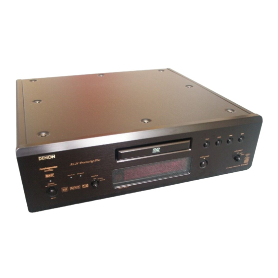
Denon DVD-9000 Service Manual
Dvd audio/video player
Hide thumbs
Also See for DVD-9000:
- Operating instructions manual (136 pages) ,
- Operating lnstructions (77 pages) ,
- Specifications (2 pages)
Advertisement
Quick Links
Download this manual
See also:
Setup Manual
MODEL
Some illustrations using in this service manual are slightly different from the actual set.
SERVICE MANUAL
DVD-9000
DVD-A1
DVD AUDIO/VIDEO PLAYER
DVD-9000
DVD-A1
16-11, YUSHIMA 3-CHOME, BUNKYOU-KU, TOKYO 113-0034 JAPAN
Telephone: 03 (3837) 5321
For U.S.A., Canada,
Europe, China, Asia,
Taiwan & Korea models
(U.S.A., Canada Model)
(Others)
Digital Player
X0136 NC 0207
Advertisement

Related Manuals for Denon DVD-9000


Summary of Contents for Denon DVD-9000
- Page 1 For U.S.A., Canada, Europe, China, Asia, Taiwan & Korea models Digital Player SERVICE MANUAL DVD-9000 MODEL (U.S.A., Canada Model) DVD-A1 (Others) DVD AUDIO/VIDEO PLAYER DVD-9000 DVD-A1 Some illustrations using in this service manual are slightly different from the actual set.
- Page 2 Optical digital output : Optical connector, 1 set Coaxial digital output : Pin jack, 1 set DENON LINK output : DENON LINK connector, 1 set Digital Audio Input: Optical digital input : Optical connector, 1 set Coaxial digital input : Pin jack, 1 set Power Supply: AC 120 V, 60 Hz (For U.S.A.
- Page 3 DVD-9000/DVD-A1 Iop Measurement (Judging for Traverse Unit Replacement) As to deciding whether optical pickup is defect or not (for replacing traverse unit), follow the steps below. 1. Judging Step (1) Disc play abnormal Problems such as disc no read, unsteady playback, etc.
- Page 4 DVD-9000/DVD-A1 DIAGNOSTICS OF OPTICAL PICKUP AND REPLACING TRAVERSE UNIT 1. Note for Handling the Laser Pick-up The protection for the damage of laser diode. If you want to change the optical device unit from any other units, you must keep the following.
- Page 5 DVD-9000/DVD-A1 DISASSEMBLY ( Follow the procedure below in reverse order when reassembling ) * Caution: Each edge inside of the metal parts may be "sharp edge", so be careful not to be injured when handling them. 1. Top/Side Cover (1) Top Cover...
- Page 6 DVD-9000/DVD-A1 3. DVD Mecha. Ass'y (1) DVD Mecha. Ass'y Remove 4 pcs of 3mm machine screw (f). [D]: Disconnect PH wire from [CX141] on the Main P.W.B. [E]: Disconnect FFC wire from [CY212] on the Interface P.W.B. [F]: Disconnect FFC wire from [CY211] on the Interface P.W.B.
- Page 7 DVD-9000/DVD-A1 5. 2ch Audio P.W.B./5.1ch Audio P.W.B. (1) 2ch Audio P.W.B. Remove 4 pcs of 3mm B-tight screw (k), 2 pcs of 3mm screw (l) on the Rear Panel, and 8 pcs of 3mm B-tight screw (m) on the top.
- Page 8 DVD-9000/DVD-A1 How to Replace Traverse Unit 1. Preparing for Replacement (1) Removing Clamp Base Damper Remove 4 pcs of 2.6mm machine screw (a), and detach Clamp Base Damper the Clamp Base Damper upward. (2) Removing Clamp Base Remove 6 pcs of 3mm P-tight screw (b), and detach the Clamp Base upward.
- Page 9 DVD-9000/DVD-A1 3. Installing Loader Plate Gear (1) Inserting Loader Set and push the Loader to the arrow direction until it Boss stops. When installing the Loader, move the Plate Gear Groove to right beforehand so as that the boss of the Plate Gear fits in the backside groove of the Loader.
- Page 10 DVD-9000/DVD-A1 5. Assembly (2) (1) Attaching Tape to Clamp Base Damper Attach acetate cloth tape to 3 projections of the Clamp Base Damper backside. Acetate Cloth Tape (2) Assembling Clamp Base Clamp Base Damper Set the Clamp Base Damper with positioning for clamper by 3 projections.
- Page 11 DVD-9000/DVD-A1 Service Mode 1. Aging Mode (1) Preparation (a) Equipment used: Any one of DVD Karaoke Disc (containing more than 10 titles), CD/Video CD (Ver1.0: None playback control), or No-menu DVD. (Setting varies according to the disc used.) (b) Unit setting: No spec other than the following procedure (Aging mode) At the tray open status, press the "POWER"...
- Page 12 DVD-9000/DVD-A1 3. P.W.B. Check Mode (1) Preparation (a) Equipment used: None (b) Unit setting: No spec other than the following procedure (2) Procedure (a) Press the "POWER" button to turn on the power while pressing the "PLAY" and "OPEN/CLOSE" buttons for DVD operation simultaneously.
- Page 13 DVD-9000/DVD-A1 TROUBLESHOOTING 1. No power (FL tube doesn't light.) When replacing µcom, µcom Check connector insertion. Re-insert the connector. Switching power (GU-3391-2): peripheral parts, or Main PCB, [CX024, CX025, CX026, CX041, perform initializing of DVD player. CX141] Main PCB (GU-3389):...
- Page 14 DVD-9000/DVD-A1 There is something wrong in Main PCB Check IC109→IC113→IC112→IC111 (GU-3389). (see Schematic Diagram) on Main PCB → Check 11MHz input of IC101 (39) pin/ (GU-3389). MCLK. There is something wrong in Main PCB Check soldering of IC106, IC703, IC706 (GU-3389).
- Page 15 DVD-9000/DVD-A1 2. No power (Both FL tube & LED don't light.) Check connector insertion. Re-insert the connector. Switching power: [CX024, CY025, CX026, CX141, CX041] Main PCB (GU-3389): [CX141, CX171] Check switching power voltages. Replace the switching power unit. [CX141]: 14P PH for Main PCB: +5V(NSW) +3.3V(NSW)
- Page 16 DVD-9000/DVD-A1 Electrical Adjustment for Video SETTING 1. Connect the monitor TV to the video output 1 terminal. 2. Connect the Oscilloscope to the Y-signal and C-signal of S2 video output terminal and each terminate at 75 Ohms. 3. Connect the Oscilloscope to the PB -signal , CB -signal and Y- signal of Component video output terminal and each terminate at 75 Ohms.
- Page 17 DVD-9000/DVD-A1 Adjustment Point & Adjustment Value Wave Wave Adjust the signal of Component Point: VR424 Adjustment Value: 1000 ±20mV video out 2 Y-signal Set the Video output to Point: VR710 PROGRESSIVE by remote control Adjustment Value: 1000 ±20mV unit. (Push the [SETUP] button, set to the mode of VIDEO SETUP.)
- Page 18 DVD-9000/DVD-A1 BLOCK DIAGRAM RS-232C FLASHROM ROT SW. DRAM DRAM FL DRIVER DVD DRIVE FRONTEND DISC SERVO ATAPI INTERFACE PANEL CONTROL [ML9207] MECHA UNIT µ-COM PROCESSOR PROCESSOR DVD DECODER [FG-180] [MN102H460B] [TA1293F] [TC9453F] [TC9469BF] RESET < PANEL CONTROL > ACT/MOTOR DRIVE CONTROL...
-
Page 19: Table Of Contents
DVD-9000/DVD-A1 SEMICONDUCTORS IC’s ES6038 (IC101) DSCK AUX[0] AUX[1] DCS0# AUX[2] DCS1# AUX[3] DB15 AUX[4] DB14 AUX[5] DB13 AUX[6] DB12 AUX[7] LOE# DB11 DB10 LCS0# LCS1# LCS2# LCS3# DMBS1 DMBS0 DRAS# LD10 DWE# LD11 DSCK_EN DCAS# LD12 LD13 DMA11 LD14 DMA10... - Page 20 DVD-9000/DVD-A1 Pin No. Pin Name Function RESET# Reset input, active low. TDMDX TDM transmit data. TDMDR TDM receive data. TDMCLK TDM clock input. TDMFS TDM frame sync. TDMTSC# TDM output enable. Audio transmit frame sync. SEL_PLL2 System and DSCK output clock frequency selection is made at the rising edge of RESET#.
-
Page 21: Aux[1]
DVD-9000/DVD-A1 Pin No. Pin Name Function PCLK2XSCN 27 MHz video output pixel clock. PCLKQSCN 13.5 MHz video output pixel clock. VSYNC# Vertical sync, active low. HSYNC# Horizontal sync, active low. 127:122 HD[5:0] Host data I/O [5:0]. HD[6] Host data I/O [6]. - Page 22 DVD-9000/DVD-A1 MX29LV160BTC-90 (IC102) Pin Description Symbol Pin Name BYTE A0~A19 Address Input Q15/A-1 Q0~Q14 Data Input/Output Q15/A-1 Q15 (Word mode)/LSB addr (Byte mode) Chip Enable Input Write Enable Input BYTE Word/Byte Selection input RESET RESET Hardware Reset Pin/Sector Protect Unlock...
- Page 23 DVD-9000/DVD-A1 SM8701BM (IC109) SM8701BM Terminal Function Pin No. Pin Name Function Control signal input. MLEN/R2 MCK/R1 MLEN/R2 In serial mode: latch enable signal In parallel mode: sampling rate select signal MDT/R0 Mode select signal. LOW: serial mode, HIGH: parallel mode RSTN ...
- Page 24 DVD-9000/DVD-A1 MN102H460B (IC201) P46,A22, CS0 P52, RE P47,A23, CS1 P51, WEH,WE P00,AD0,D0 P50, WEL P01,AD1,D1 PC7,NBRACK P02,AD2,D2 PC6,NBREQ P03,AD3,D3 P97,AN15,TM20IB P96,AN14,TM15O,TM19IB P95,AN13,TM13O,TM2I P04,AD4,D4 P94,AN12,TM11O,TM4I P05,AD5,D5 AVDD P06,AD6,D6 VREFH P07,AD7,D7 P93,AN11 P10,AD8,D8 P92,AN10 P11,AD9,D9 P91,AN9 P12,AD10,D10 P90,AN8 PD0,RTP0 PD5,RTP5 TOP VIEW...
- Page 25 DVD-9000/DVD-A1 AK4101VQ (IC205) AK4101VQ Terminal Function Pin No. Pin Name Function Power down and reset pin MCLK Master clock input pin SDTI1 Audio serial data input 1 pin SDTI2 Audio serial data input 2 pin SDTI3 Audio serial data input 3 pin...
- Page 26 DVD-9000/DVD-A1 ADSPMEL322 (IC207) HAD0 HAD1 HAD2 HAD3 HAD4 HAD5 DDEXT HAD6 HAD7 HAD8 DDEXT HAD9 HAD10 HAD11 HAD12 TOP VIEW DDINT DDEXT HAD13 HAD14 HAD15 HA16 HACK_P DDEXT HACK OPMODE HCMS DDINT HCIOMS HALE TRST RESET XC2S30-5VQ100C (IC711) VCCO VCCO...
- Page 27 DVD-9000/DVD-A1 TA1293F (IC501) P1TN DFTN P1TP P1FN P1FP LDP1 GNDR P1DI P1CI P1BI P1AI LDP2 P2AI P2BI P2CI VccS P2DI RFSW GNDS P2FP P2FN P2TP P2TN VccP TA1293F Terminal Function Pin No. Pin Name Function GNDP GND pin LDO2 O Drive pin...
- Page 28 DVD-9000/DVD-A1 Pin No. Pin Name Function Used connecting with VrA O Servo addition output Used in open O TE output O TE output Used connecting with VrA Used connecting with VrA Used connecting with VrA Used connecting with VrA Used connecting with VrA...
- Page 29 DVD-9000/DVD-A1 TC9453F (IC505) Analog Digital to Driver 1bit DAC from Digital Output for CD-DA RF-Amp. Servo (servo signal) Clock from RF Signal Output RF-Amp. Sync Data Out Process (RF signal) MPU I/F 1Mbit DRAM LPFN LPFO PVREF VCOREF VCOF PVDD...
- Page 30 DVD-9000/DVD-A1 TC9453F Terminal Function Pin No. Pin Name Function GND for DAC O R-ch output signal, Analog output pin Power for DAC O Amp ref. signal output, Analog input pin O L-ch output signal, Analog output pin GND for DAC GND for oscillator X’tal osc.
- Page 31 DVD-9000/DVD-A1 Pin No. Pin Name Function 3.3V digital power O DVD/CD data output GND for 5V O DVD/CD data output O DVD/CD data output O DVD/CD data output O DVD/CD data output 3.3V digital GND O DVD/CD data output O DVD/CD data output...
-
Page 32: Lcs0
DVD-9000/DVD-A1 Pin No. Pin Name Function TESM5 Test pin, Connect to GND TESM6 Test pin, Connect to GND TESM7 Test pin, Open TESM8 Test pin, Open 3.3V digital GND CFC1 O VCO frequency control signal, Analog output pin CFC2 O VCO frequency control signal, Analog output pin O Phase comparator offset adj. -
Page 33: Lcs1
DVD-9000/DVD-A1 TC9469BF (IC508) Buffer DRAM 256kw/128kw/64kw (4Mbit/2Mbit/1Mbit) CSEL /PDIAG./DASP (H-IF) CD-IF & Buffer IORDY PSYCN.PDROM DVD-IF Address HDRQ PDCK Input /HDAK Selecter HEDda PDA8 H-FIFO /IOCS16 (64B) HD15-0 HSYC /HRD./HWR /HCS3./HCS1 SUB-IF Input HA2-0 SBDa PDA(7:0) Convert SBQa INTRQ H Interrupt... - Page 34 DVD-9000/DVD-A1 TC9469BF Terminal Function Pin No. Pin Name Function GND pin Host address 2 input: IDE sig. DA2, TTL level input, pull-up R built-in /HCS1 Chip select 1 input: IDE sig. /CS1FX, TTL level input, pull-up R built-in HCS3 Chip select 3 input: IDE sig.
-
Page 35: Lcs2
DVD-9000/DVD-A1 Pin No. Pin Name Function PSYCN Sync signal input PDA8 Parallel data 8 input PDA7 Parallel data 7 input PDA6 Parallel data 6 input PDA5 Parallel data 5 input GND pin PDA4 Parallel data 4 input PDA3 Parallel data 3 input... - Page 36 DVD-9000/DVD-A1 Pin No. Pin Name Function HD11 HD12 I/O Host data in/output (HD[0:15]:IDE sig. DD[0:15]), TTL level, tri-state out, pull-up R built-in HD13 HD14 Power pin GND pin HD15 I/O Host data in/output (HD[0:15]:IDE sig. DD[0:15]) HDRQ O Data request output: IDE sig. DMARQ, tri-state out, drive-ability 12mA /HWR Host write signal input: IDE sig.
- Page 37 DVD-9000/DVD-A1 TMP95FY64F (IC511) P33/A11 P05/D5 P32/A10 P04/D4 P31/A9 P03/D3 P30/A8 P02/D2 P47/A7 P01/D1 P46/A6 P00/D0 P45/A5 P44/A4 P96/TOA/TOB P43/A3 P95/TIB/INT8 P42/A2 INT7 P41/A1 P93/TO9 P40/A0 P92/TO8 P50/RD P91/TI9/INT6 P51/WR P90/TI8/INT5 P52/HWR P75/TO7/INT4 (GND)VSS P74/TO5 PA0/AN0 P73/TI4/INT3 PA1/AN1 P72/TO3/INT2 PA2/AN2 P71/TO1...
- Page 38 DVD-9000/DVD-A1 Pin No. Pin Name Symbol Function INT3 FG signal input from TA8493F BRKN O Brake signal output to TA8493F Not used INT5 SLIDE_PULSE Pulse counter input of slide P-LOW O PLL filter switching output PLLD Not used P-HIGH O PLL filter switching output ...
- Page 39 DVD-9000/DVD-A1 SiI504CM208 (IC701, 703) HostAddr6 RSVD RSVD HostAddr7 GNDCore HostMode MemClk VDDCore GNDCore HostClk VDDCore GNDCore HostData15\VidlnData19 MemData14 HostData14\VidlnData18 MemData13 MemData12 HostData13\VidlnData17 MemData11 HostData12\VidlnData16 MemData10 GNDCore VDDCore GNDIO MemData9 HostData11\VidlnData15 MemData8 HostData10\VidlnData14 HostData9\VidlnData13 PuPdDis VDDIO HostData8\VidlnData12 MemData0 RSVD MemData1 HostData7\VS...
- Page 40 DVD-9000/DVD-A1 Pin No. Pin Name Function 16, 26, 73, 74, 89, 117, 132, VDDIO 3.3V I/O Power. 135, 182, 189, 22~25, 27~32 Green_Y[9:0] Green Data (RGB output mode); Y Data (YCrCb output mode) 34~39, 42~45 Red_Cr[9:0] Red Data (RGB output mode); Cr Data (YCrCb output mode)
- Page 41 DVD-9000/DVD-A1 64M SDRAM (IC702) W986432AH W986432AH Terminal Function Pin No. Pin Name Function DQ15 25~27, 60~66, 24 A0-A10 Address for row and column Bank Select to activate during row DQ14 22, 23 BS0, BS1 address latch time DQ13 2, 4, 5, 7, 8, 10, 11 ,13,...
- Page 42 DVD-9000/DVD-A1 LC89055W-RA8 (IC501) LC89055W-RA8 Terminal Function Pin Name Function DISEL Data input terminal (select input pin of DIN0, DIN1) DOUT Input bi-phase data through output terminal DIN0 Amp built-in coaxial/optical input correspond data input terminal DIN1 Amp built-in coaxial/optical input correspond data input terminal...
- Page 43 DVD-9000/DVD-A1 DXP7001AF (IC701) DXP7001AF Terminal Function Pin Name Description Pin Name Description − P24L − /Lambda-processor Lch 24 Microcomputer Interface Data bit Output *1, *2 − P23L − /Lambda-processor Lch 23 Microcomputer Interface Clock bit Output *1, *2 − P22L −...
- Page 44 DVD-9000/DVD-A1 ADV7304 (IC421, 706) VDD_IO S_BLANK SET 1 VREF COMP1 DAC A DAC B DAC C TOP VIEW AGND DAC D DGND DAC E DAC F COMP2 SET 2 EXT_LF RESET ADV7304 Terminal Function Pin No. Pin Name Function Digital power supply.
- Page 45 DVD-9000/DVD-A1 DF1704 (IC417, 418) DF1704 Terminal Function Name Function LRCIN BCKIN Serial audio data input BCKO BCKIN Bit clock input for serial audio data WCKO Input audio data format select Input audio data word select Input audio data word select...
- Page 46 DVD-9000/DVD-A1 ML9207-01 (IC601) COM22 COM21 COM20 SEG1 COM19 SEG2 COM18 SEG3 COM17 SEG4 COM16 SEG5 COM15 SEG6 COM14 SEG7 COM13 SEG8 COM12 SEG9 COM11 SEG10 COM10 SEG11 COM9 SEG12 COM8 SEG13 COM7 SEG14 COM6 SEG15 COM5 SEG16 COM4 SEG17 SEG18...
- Page 47 DVD-9000/DVD-A1 BA5952AFP (IC504) Terminal Function V I N F C M U T E C F C E r r 1 B I A S Pin No. Name Function Pin No. Name Function C F C E r r 2...
- Page 48 DVD-9000/DVD-A1 SN74LV157APW (IC702) TC74HCT7007AF (IC206, 209, 502) SN74LV74APW (IC704) TC74HC157AF(IC512) " 1CLR 14 V SELECT 2CLR STROBE INPUTS INPUTS OUTPUT OUTPUT INPUTS INPUTS OUTPUT & OUTPUT SN74LV04APW (IC208, 514, 515, 703) TC74HC123AF (IC422, 708) TC4053BF (IC807, 808) TC74HCT04AF (IC410, 507, 619)
- Page 49 DVD-9000/DVD-A1 TRANSISTORS DTC114EK DTA114EK 2SA1015GR DTA114EK DTC114EK DTC143EK DTA114TK 2SC1740S (S) DTA114TK DTC143EK DTC143TK DTA124EK 2SC2878 (A/B) DTA124EK DTC143TK 2SB709A KTC2875B 2SD468 (C) 2SD601A NPN Type PNP Type FRONT VIEW VIEW VIEW 10kohm / W 10kohm / W DTC114EK 10kohm / W...
- Page 50 DVD-9000/DVD-A1 FL DISPLAY 17-ST-044NK (FL101) COLOR ILLUMINATION Reddish Orange ----- Above pattern part Green ------------------ Other PIN CONNECTION PIN NO. CONNECTION NOTE 1) F-,F+ ---------- Filament 2) NP ------------- No pin PIN NO. 3) NX ------------- No extend pin 4) DL ------------ Datum line...
- Page 51 DVD-9000/DVD-A1 PRINTED WIRING BOARD GU-3389 MAIN P .W.B. UNIT Ass'y COMPONENT SIDE...
- Page 52 DVD-9000/DVD-A1 GU-3389 MAIN P .W.B. UNIT Ass'y FOIL SIDE...
- Page 53 DVD-9000/DVD-A1 GU-3390 VIDEO/AUDIO P .W.B. UNIT Ass'y COMPONENT SIDE...
- Page 54 DVD-9000/DVD-A1 GU-3390 VIDEO/AUDIO P .W.B. UNIT Ass'y FOIL SIDE...
- Page 55 DVD-9000/DVD-A1 GU-3391 AUDIO/POWER P .W.B. UNIT Ass'y COMPONENT SIDE...
- Page 56 DVD-9000/DVD-A1 GU-3391 AUDIO/POWER P .W.B. UNIT Ass'y FOIL SIDE...
- Page 57 DVD-9000/DVD-A1 GU-3410 KEY/DISPLAY P .W.B. UNIT Ass'y COMPONENT SIDE FOIL SIDE...
- Page 58 DVD-9000/DVD-A1 NOTE FOR PARTS LIST Part indicated with the mark " " are not always in stock and possibly to take a long period of time for supplying, or in some case supplying of part may be refused. When ordering of part, clearly indicate "1" and "I" (i) to avoid mis-supplying.
- Page 59 Note : The symbols in the column “Remarks” indicate the following destinations. E2 : Europe model E1 : Asia model 1U-3389 MAIN UNIT ASS'Y G1C : China model E3 : DVD-9000 model Ref. No. Part No. Part Name Remarks Ref. No.
- Page 60 DVD-9000/DVD-A1 Ref. No. Part No. Part Name Remarks Ref. No. Part No. Part Name Remarks R186,187 247 2018 903 Carbon chip 0 ohm 1/16W RM73B--0R0KT R523 247 2004 988 Carbon chip 82 ohm 1/16W RM73B--820JT R189-191 247 2018 903 Carbon chip 0 ohm 1/16W...
- Page 61 DVD-9000/DVD-A1 Ref. No. Part No. Part Name Remarks Ref. No. Part No. Part Name Remarks R633 244 2051 945 Metal oxide 1 ohm 1W(NB) RS14B3A010JNBST(S) R787 247 2003 989 Carbon chip 33 ohm 1/16W RM73B--330JT R634 244 2052 960 Metal oxide 220 ohm 1W(NB) RS14B3A221JNBST(S)
- Page 62 DVD-9000/DVD-A1 Ref. No. Part No. Part Name Remarks Ref. No. Part No. Part Name Remarks C112-122 257 0512 903 Ceramic chip 0.1uF/25V CK73F1E104ZT C214 257 0503 967 Ceramic chip 15pF/50V CC73CH1H150JT C123 254 4464 906 Electrolytic 100uF/6.3V CE67C0J101MT C215 254 4465 918 Electrolytic 47uF/16V...
- Page 63 DVD-9000/DVD-A1 Ref. No. Part No. Part Name Remarks Ref. No. Part No. Part Name Remarks C527 257 0509 929 Ceramic chip 1000pF/50V CK73B1H102KT C634 257 4010 906 Electrolytic 100uF/16V CE67C1C101MT C528,529 257 0512 903 Ceramic chip 0.1uF/25V CK73F1E104ZT C635,636 257 0512 903 Ceramic chip 0.1uF/25V...
- Page 64 DVD-9000/DVD-A1 GU-3390E VIDEO/AUDIO UNIT ASS'Y Ref. No. Part No. Part Name Remarks Q'ty Ref. No. Part No. Part Name Remarks OTHER PARTS GROUP SEMICONDUCTORS GROUP CX031 205 0863 936 3P PH Connector base(L) IC421 262 3124 002 IC ADV7304 CX051...
- Page 65 DVD-9000/DVD-A1 Ref. No. Part No. Part Name Remarks Ref. No. Part No. Part Name Remarks TR616 269 0082 902 Transistor DTC114EKT96 R458-463 247 2005 987 Carbon chip 220 ohm 1/16W RM73B--221JT TR617 273 0426 907 Transistor 2SC2412KLNT146 R464,465 247 2005 903 Carbon chip 100 ohm 1/16W RM73B--101JT...
- Page 66 DVD-9000/DVD-A1 Ref. No. Part No. Part Name Remarks Ref. No. Part No. Part Name Remarks R575-577 247 2018 903 Carbon chip 0 ohm 1/16W RM73B--0R0KT R702-708 247 2018 903 Carbon chip 0 ohm 1/16W RM73B--0R0KT R578 247 2007 943 Carbon chip 1 kohm 1/16W...
- Page 67 DVD-9000/DVD-A1 Ref. No. Part No. Part Name Remarks Ref. No. Part No. Part Name Remarks R825 247 2006 986 Carbon chip 560 ohm 1/16W RM73B--561JT R952,953 247 2009 983 Carbon chip 10 kohm 1/16W RM73B--103JT R826 247 2009 983 Carbon chip 10 kohm 1/16W RM73B--103JT...
- Page 68 DVD-9000/DVD-A1 Ref. No. Part No. Part Name Remarks Ref. No. Part No. Part Name Remarks C431,432 257 0512 903 Ceramic chip 0.1uF/25V CK73F1E104ZT C538 257 0509 929 Ceramic chip 1000pF/50V CK73B1H102KT C434 257 0509 903 Ceramic chip 820pF/50V CK73B1H821KT C541...
- Page 69 DVD-9000/DVD-A1 Ref. No. Part No. Part Name Remarks Ref. No. Part No. Part Name Remarks C667,668 256 1054 001 Metalized 1uF/50V CF93B1H105K(GSG) C828 254 4533 934 Electrolytic 220uF/6.3V CE04W0J221MT SMG/RE3 C669,670 254 4356 742 Electrolytic 470uF/50V CE04W1H471(ARS) C829 257 0512 903 Ceramic chip 0.1uF/25V...
- Page 70 DVD-9000/DVD-A1 Ref. No. Part No. Part Name Remarks Ref. No. Part No. Part Name Remarks Q'ty C905 254 4538 939 Electrolytic 47uF/16V CE04W1C470MT SMG/RE3 FB601 235 0130 903 Chip emifil (11A121) For E2 FB603-606 235 0136 907 FBMJ1608HS280NT For E1,G1C,E2 C906 257 0512 903 Ceramic chip 0.1uF/25V...
- Page 71 DVD-9000/DVD-A1 GU-3391 AUDIO/POWER UNIT ASS'Y Ref. No. Part No. Part Name Remarks Ref. No. Part No. Part Name Remarks SEMICONDUCTORS GROUP ZD901 276 0457 904 Zener diode HZS4C-1TD IC401,402 262 2530 914 IC PCM1704U/2K TH901 279 0044 002 Thermistor NTH11D8R0LA...
- Page 72 DVD-9000/DVD-A1 Ref. No. Part No. Part Name Remarks Ref. No. Part No. Part Name Remarks CAPACITORS GROUP C526 257 0512 903 Ceramic chip 0.1uF/25V CK73F1E104ZT C528 257 0512 903 Ceramic chip 0.1uF/25V CK73F1E104ZT C401,402 257 0509 929 Ceramic chip 1000pF/50V...
- Page 73 DVD-9000/DVD-A1 Ref. No. Part No. Part Name Remarks Ref. No. Part No. Part Name Remarks Q’ty C965 257 0511 904 Ceramic chip 0.01uF/50V CK73F1H103ZT L907 235 0142 917 Inductor 4.7uH C966 254 4368 947 Electrolytic 220uF/25V CE04W1E221MT(ASF) L909 235 0142 917 Inductor 4.7uH...
- Page 74 DVD-9000/DVD-A1 GU-3410 KEY/DISPLAY UNIT Ref. No. Part No. Part Name Remarks Ref. No. Part No. Part Name Remarks Q'ty SEMICONDUCTORS GROUP OTHER PARTS GROUP IC601 262 3048 007 IC ML9207-01GP CW041 203 6582 008 4P PH-SAN Connector cord IC603 499 0303 004 IC GP1UM271XK...
- Page 75 DVD-9000/DVD-A1 EXPLODED VIEW Rear View JP Model Only E2 Model Only G1C/E1/E2/E1K Model Only E2 Model Only WARNING: Parts marked with this symbol have critical characteristics. Use ONLY replacement parts recommended by the manufacturer.
-
Page 76: Ld13
Note : The symbols in the column “Remarks” indicate the following destinations. PARTS LIST OF EXPLODED VIEW E2 : Europe model E1 : Asia model E1K : Korea model G1C : China model E3 : DVD-9000 model E1T : Taiwan model Ref. No. Part No. Part Name Remarks Q'ty Ref. - Page 77 DVD-9000/DVD-A1 Ref. No. Part No. Part Name Remarks Q'ty SCREWS 102 471 3304 028 Screw 3x8 CBS-B 103 471 3832 008 Screw 3X8 CBS-CU For Gold model 106 477 0064 107 Fixing screw For Black model 103 473 7015 018 Screw 3x8 CBTS (S)-B...
- Page 78 DVD-9000/DVD-A1 EXPLODED VIEW OF DVD MECHANISM...
- Page 79 DVD-9000/DVD-A1 PARTS LIST OF DVD MECHANISM Ref. No. Part No. Part Name Remarks Q'ty Ref. No. Part No. Part Name Remarks Q'ty 1 411 1988 101 Mecha chassis SCREWS 2 431 0426 503 Plate gear 50 471 9057 007 Special screw M1.7 9KA 2A40 3D Gear base sub ass'y 9KM 01T1 32 Screw 2.6x2.5 CBS-NI...
- Page 80 DVD-9000/DVD-A1 POINTS OF GREASING (1/2) MOLYKOTE EM-30L 0.1mg x 4 points MOLYKOTE EM-30L 0.1mg MOLYKOTE EM-30L 0.1mg x 3 points MOLYKOTE EM-30L 0.1mg x 4 points MOLYKOTE EM-30L 0.1mg x 4 points MOLYKOTE EM-30L 0.1mg x 3 points MOLYKOTE EM-30L 0.1mg...
- Page 81 DVD-9000/DVD-A1 POINTS OF GREASING (2/2) MOLYKOTE EM-30L 0.1mg x 4 points HANARL FL777 0.1mg MOLYKOTE EM-30L MOLYKOTE EM-30L 0.1mg 0.1mg x 5 points MOLYKOTE EM-30L 0.3mg MOLYKOTE EM-30L 0.1mg 40~50mm HANARL UD777 0.1mg MOLYKOTE EM-30L 0.1mg...
-
Page 82: Ld14
E1 : Asia model E1K : Korea model G1C : China model E3 : DVD-9000 model E1T : Taiwan model PARTS LIST OF PACKING & ACCESSORIES Parts indicated with the mark " " is not illustrated in the exploded view. - Page 83 DVD-9000/DVD-A1 WIRING DIAGRAM GU-3390-5 CY034 SCART PWB UNIT (E2 MODEL ONLY) CY102 AC IN CX024 CX102 10P TUCP CX025 GU-3390-3 2P VH GU-3390-2 2P VH VIDEO PWB UNIT I/F PWB UNIT 3P PH CX026 CX034 CY033 2P VH CY131 CY025...
- Page 84 DVD-9000/DVD-A1 MEASURING METHOD AND WAVEFORMS To check the waveforms on the Servo P.W.B., the GND ( ) probe of the oscilloscope to Vref point. (Except for Inner SW, TRVSW) * For , connect the GND (−) probe to "GND". &...
- Page 85 DVD-9000/DVD-A1 WAVEFORMS GU-3389-1 MAIN P.W.B. DVD PLAY (INNER) DVD PLAY Disc DVDT-S01 HF (RFI) Vref V = 0.5 V/div CD PLAY (INNER) CD PLAY Disc TCD-784A HF (RFI) Vref V = 0.5 V/div SERCH TO OUTER CHAPTER (DVD/CD) LOADING PLAY...
- Page 86 DVD-9000/DVD-A1 GU-3390-1 AUDIO P.W.B.
- Page 87 DVD-9000/DVD-A1...
- Page 88 DVD-9000/DVD-A1 GU-3390-2 VIDEO P.W.B. 75Ω terminate 75Ω terminate 75Ω terminate...
- Page 89 DVD-9000/DVD-A1 GU-3390-3 I/F P.W.B. GU-3391-2 DIGITAL POWER P.W.B. 3391- 3391- 3391- 3391- 3391-...
- Page 90 DVD-9000/DVD-A1 SCHEMATIC DIAGRAMS (1/9) For the Waveforms marked with numbers , refer to page 85 (WAVEFORMS). WARNING: Parts marked with this symbol have critical characteristics. Use ONLY replacement parts recommended by the manufacture. CAUTION: Before returning the unit to the customer, make sure you make either (1) a leakage current check or (2) a line to chassis resistance check.
- Page 91 DVD-9000/DVD-A1 SCHEMATIC DIAGRAMS (2/9) WARNING: Parts marked with this symbol have critical characteristics. Use ONLY replacement parts recommended by the manufacture. CAUTION: Before returning the unit to the customer, make sure you make either (1) a leakage current check or (2) a line to chassis resistance check. If the leakage current exceeds 0.5 milliamps, or if the resistance from chassis to either side...
- Page 92 DVD-9000/DVD-A1 SCHEMATIC DIAGRAMS (3/9) For the Waveforms marked with numbers or symbols, refer to page 87 (WAVEFORMS). WARNING: Parts marked with this symbol have critical characteristics. Use ONLY replacement parts recommended by the manufacture. CAUTION: Before returning the unit to the customer, make sure you make either (1) a leakage current check or (2) a line to chassis resistance check.
- Page 93 DVD-9000/DVD-A1 SCHEMATIC DIAGRAMS (4/9) A5 A6 A5 A6 A5 A6 WARNING: NOTICE For the Waveforms marked with numbers or symbols, refer to page 86 (WAVEFORMS). ALL RESISTANCE VALUES IN OHM. k=1,000 OHM M=1,000,000 OHM Parts marked with this symbol have critical characteristics.
- Page 94 DVD-9000/DVD-A1 SCHEMATIC DIAGRAMS (5/9) Progre only Progre only Progre only terminate terminate terminate For the Waveforms marked with numbers or symbols, refer to page 88 (WAVEFORMS). WARNING: Parts marked with this symbol have critical characteristics. Use ONLY replacement parts recommended by the manufacture.
- Page 95 DVD-9000/DVD-A1 SCHEMATIC DIAGRAMS (6/9) For the Waveforms marked with numbers or symbols, refer to page 89 (WA VEFORMS). WARNING: Parts marked with this symbol have critical characteristics. Use ONLY replacement parts recommended by the manufacture. CAUTION: Before returning the unit to the customer, make sure you make either (1) a leakage current check or (2) a line to chassis resistance check.
- Page 96 DVD-9000/DVD-A1 SCHEMATIC DIAGRAMS (7/9) A14 A15 For the Waveforms marked with numbers or symbols, refer to page 86 ~ 87 (WAVEFORMS). B LINE SIGNAL LINE NOTICE ALL RESISTANCE VALUES IN OHM. k=1,000 OHM M=1,000,000 OHM ALL CAPACITANCE VALUES IN MICRO FARAD. P=MICRO-MICRO FARAD EACH VOLTAGE AND CURRENT ARE MEASUERD AT MO SIGNAL INPUT CONDITION.
- Page 97 DVD-9000/DVD-A1 SCHEMATIC DIAGRAMS (8/9) 3391- POWER ON : +5V St-by : 0V 3391- POWER ON/St-by : +5V 3391- 3.6V 3391- 3391- GND for Primary circuit POWER ON : 3.2V St-by : +0V For the Waveforms marked with numbers or symbols,...
- Page 98 DVD-9000/DVD-A1 SCHEMATIC DIAGRAMS (9/9) B LINE NOTICE ALL RESISTANCE VALUES IN OHM. k=1,000 OHM M=1,000,000 OHM ALL CAPACITANCE VALUES IN MICRO FARAD. P=MICRO-MICRO FARAD EACH VOLTAGE AND CURRENT ARE MEASUERD AT MO SIGNAL INPUT CONDITION. CIRCUIT AND PARTS ARE SUBJECT TO CHANGE WITHOUT PRIOR NOTICE.
Need help?
Do you have a question about the DVD-9000 and is the answer not in the manual?
Questions and answers