Table of Contents
Advertisement
Quick Links
See also:
User Manual
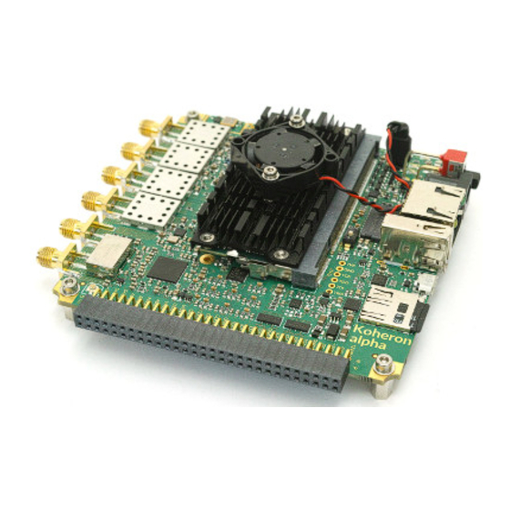
ALPHA250
ALPHA250 - User Guide
Getting started
Warnings
The ALPHA250 power supply must be turned off before connecting or disconnecting: * the micro-SD card *
peripherals on the expansion connector
Turn on the board
First, insert the micro-SD card into the micro-SD slot. Then connect the 12V jack of the power supply. The power
good green LED (PWGD) and the FPGA done orange LED (DONE) indicate the system has correctly started.
Communicating with the board
LAN
The ethernet port is the main communication interface with the ALPHA250. It can be connected to a local network
via a router
or
directly to a
computer. The last 8 bits of the IP address are displayed on the 8 user LEDs.
Serial interface
The serial UART debugging interface can be accessed by the micro USB connector. The required steps are described
here.
Important note: Turn on the board first and wait for the board to boot before connecting the serial cable.
Connectors
1 / 13
www.koheron.com
Advertisement
Table of Contents

Related Manuals for Koheron ALPHA250

Summary of Contents for Koheron ALPHA250
-
Page 1: Getting Started
LED (PWGD) and the FPGA done orange LED (DONE) indicate the system has correctly started. Communicating with the board The ethernet port is the main communication interface with the ALPHA250. It can be connected to a local network via a router directly to a computer. -
Page 2: Micro Usb
The external supply connector is a jack with 1.95 mm center pin and 6 mm outer diameter. Only 12 V must be supplied on this connector. Running the ALPHA250 requires at least 1 A. More current may be required depending on the load on the expansion connector. - Page 3 ALPHA250 ALPHA250 expansion connector It contains: Power supplies. 12 V from external supply. 5 V up to 1 A (shared with USB 2.0 connector). + 3.3 V up to 800 mA, sequenced with I/Os supply. - 3.3 V up to 500 mA.
- Page 4 ALPHA250 ALPHA250 RF ADC interface. The encoding clock of the ADC is provided by the of the clocking system. The output data are interfaced RF_ADC_CLK to the I/O Bank 34 of the FPGA. It consists of 14 LVDS pairs operating in double data rate. The maximum transfer rate per LVDS pair is thus 500 Msps.
-
Page 5: Precision Adc
VCO (2.37 to 2.6 GHz) onto the VCXO. A set of clock dividers allows to produce up to six clocks at desired frequencies. ALPHA250 clocking system. The clock generator is designed to accept 10 MHz reference clocks. The reference clock sources are: The CLKI SMA input on the board. -
Page 6: Precision Dac
Temperature sensors The ALPHA250 has two high-accuracy temperature sensors (TMP116) with an accuracy of ±0.2 °C over -10 °C to +85 °C. One sensor is placed near the voltage reference (T0 highlighted in blue) to allow temperature compensation in high precision measurements. -
Page 7: Power Monitors
I2C0 driver. The EEPROM is divided into two parts. The lower addresses are used by Koheron to store identification and calibration data. The higher addresses (above 0x1000) are for user applications. The EEPROM map addressing is given in the table below. -
Page 8: Rf Adc Parallel Bus
ALPHA250 Zynq I/Os The Zynq XC7Z020-2CLG400I has 2 I/O banks for the programmable logic (Banks 34 and 35) with 48 IOs each. One bank (Bank 0) is dedicated to the processing system with a multiplexed I/O (MIO) interface. The set of peripherals and interface buses is depicted below. -
Page 9: Rf Dac Parallel Bus
ALPHA250 set_property PACKAGE_PIN W15 [get_ports {adc_1_n[4]}] set_property PACKAGE_PIN V15 [get_ports {adc_1_p[4]}] set_property PACKAGE_PIN T15 [get_ports {adc_1_n[5]}] set_property PACKAGE_PIN T14 [get_ports {adc_1_p[5]}] set_property PACKAGE_PIN Y17 [get_ports {adc_1_n[6]}] set_property PACKAGE_PIN Y16 [get_ports {adc_1_p[6]}] RF DAC parallel bus The RF DAC is interfaced to the Bank 35 by a LVCMOS 3V3 parallel bus. The data for each channel are transferred on a 16 line sub-bus. - Page 10 ALPHA250 Configuration SPI bus. Constraint file The configuration SPI bus pins are connected to Bank 34 with 1.8 V LVCMOS signals. # Configuration SPI (Bank 34) set_property IOSTANDARD LVCMOS18 [get_ports spi_cfg_*] set_property PACKAGE_PIN R17 [get_ports spi_cfg_sdo] set_property PACKAGE_PIN R16 [get_ports spi_cfg_sdi]...
-
Page 11: Precision Adc Spi Bus
ALPHA250 The transferred data must be wired to the pin. The transfer is triggered on the pin falling s_axis_tdata s_axis_tvalid edge. The core is controlled via the SpiConfig driver. Precision ADC SPI bus A dedicated SPI is used for the communication with the precision ADC. The bus is connected to PL I/Os on bank 34. - Page 12 The constraints file for the PS is: set_property CFGBVS GND [current_design] set_property CONFIG_VOLTAGE 1.8 [current_design] I2C0 This bus is used on the ALPHA250 internally and is not accessible from the expansion connector. The I2C0 bus addressing is: * : Secure EEPROM * : RTC registers *...
- Page 13 ALPHA250 The USB 2 connector is interfaced with the core. USB0 The SD card is interfaced with the core. UART0 The serial port debugging USB interface connects to the core. UART0 13 / 13 www.koheron.com...
Need help?
Do you have a question about the ALPHA250 and is the answer not in the manual?
Questions and answers