Table of Contents
Advertisement
Advertisement
Table of Contents

Related Manuals for Sharp LC-32SV40U


Summary of Contents for Sharp LC-32SV40U
- Page 1 SERVICE MANUAL LCD COLOR TELEVISION MODEL: LC-32SV40U LC-42SV50U LC-46SV50U...
-
Page 2: Table Of Contents
CONTENTS SAFETY PRECAUTION IMPORTANT SERVICE SAFETY PRECAUTION ................………………………2 CHAPTER 1. SPECIFICATIONS [1] SPECIFICATIONS............................4 [2] DIMENSIONS..............................6 CHAPTER 2. REMOVING OF MAJOR PARTS [1] REMOVING OF MAJOR PARTS ......................9 CHAPTER 3. ADJUSTMENT PROCEDURE [1] ADJUSTMENT PROCEDURE ....................... 32 [2] SERVICE MODE ............................ 37 [3] SOFTWARE UPGRADE PROCEDURE .................... -
Page 5: Specifications
CHAPTER 1. OPERATION MANUAL [1] SPECIFICATIONS Item Model: LC-32SV40U LCD screen size 32 inches diagonal Resolution 1366 x 768 TV-standard American TV Standard ATSC/NTSC System VHF/UHF VHF 2-13ch, UHF 14-69ch CATV 1-125ch (non-scrambled channel only) Digital Terrestrial Receiving Broadcast 2-69ch... - Page 6 Item Model: LC-42SV50U Model: LC-46SV50U LCD screen size 42 inches diagonal 46 inches diagonal Resolution 1920 x 1080 1920 x 1080 TV-standard American TV Standard ATSC/NTSC System VHF/UHF VHF 2-13ch, UHF 14-69ch CATV 1-125ch (non-scrambled channel only) Digital Terrestrial Receiving Broadcast 2-69ch function...
-
Page 7: Dimensions
[2]DIMENSIONS LC-32SV40U Wall Mounting Screw type VESA compatible wall-bracket TV screen size (Inchs) (millimeters) ( W x H) 32"(LC-32SV40U) 200X200mm Metric 6x12mm... - Page 8 LC-42SV50U wall mounting VESA-compatible wall bracket TV screen size (Inches) Screw type (millimeters)(W*H) 42'' 200*200mm Metric 8*22mm...
- Page 9 LC-46SV50U...
-
Page 10: Removing Of Major Parts
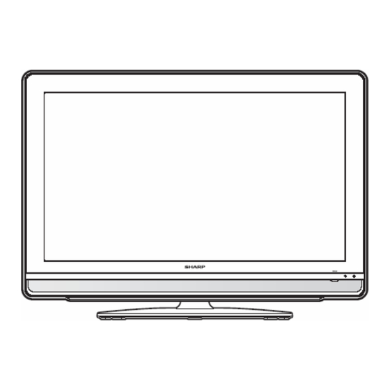
CHAPTER2. Removing of Major Parts LC-32SV40U 1.Assy/PanelRemoval Notes: Please put your machine on soft material to avoid to scrape panel when you disassemble it. Front view Fig.1 Back view Fig.2 Step 1. Remove the Base Assy. 1. Remove the base as Fig.3. - Page 11 Fig.3 Step 2. Remove the REAR COVER Assy. 1. Remove the 13 screws,around the REAR COVER as Fig.4. Fig.4 2. Remove the 2 screws at the IO area as Fig.5.
- Page 12 Fig.5 3. Remove the 3 screws to release AC cable as Fig.6 .Fig.7 Fig.6 Fig.7 Step 3. Remove the Main, Power ,IR board , Key Pad ASSY, and the Speakers.
- Page 13 Fig.8 1. Remove the 4 screws and disconnect 4 cables .Detach the Main board ASSY as Fig.9...
- Page 14 Fig.9 2. Remove the 5screws and 2 Cables. Detach the Power board as Fig.10.
- Page 15 Fig.10 3. .Detach the IR board as Fig.11. Fig.11...
- Page 16 4. Detach the Key Pad ASSY as Fig.12. Pull Fig.12 5. Detach the Speakers as Fig.13. Fig.14. Fig.13 Fig.14...
- Page 17 Step 4. Remove TOP VESA,VESA PLATE,AND BASE SUPPORT,. 1.Remove the 6 screws. Detach the TOP VESA and VESA PLATE as Fig.15 Fig.15 2.Remove the 4 screws. Detach the BASE SUPPORT as Fig.16 Fig.16 Step 5. Remove PANEL module. Remove the 2 screws at the bottom side of panel as Fig.17. Fig.17...
- Page 18 LC-42SV50U 1. Assy/Panel Removal Notes: Please put your machine on soft material to avoid to scrape panel when you disassemble it. Front view Fig.1 Back view Fig.2 Step 1. Remove the Base Assy. 2. Remove the base as Fig.3. Remove the 8 screws as Fig.3 and pull out the base. Fig.3...
- Page 19 Step 2. Remove the REAR COVER Assy. 1. Remove the 18 screws,around the REAR COVER as Fig.4. Fig.4 2. Remove the 2 screws at the IO area as Fig.5. Fig.5...
- Page 20 3. Remove the 3 screws to release AC cable as Fig.6 .Fig.7 Fig.6 Fig.7 Step 3. Remove the Main, Power ,IR board , Key Pad ASSY, and the Speakers. Fig.8...
- Page 21 1. Remove the 12 screws and disconnect 4 cables .Detach the Main board ASSY as Fig.9 Fig.9 2. Remove the 6screws and 2 Cables. Detach the Power board as Fig.10. Fig.10...
- Page 22 3. Detach the IR board as Fig.11. Fig.11 4. Remove the 2screws ,Detach the Key Pad ASSY as Fig.12. Fig.12...
- Page 23 5. Detach the Speakers as Fig.13. Fig.14. Fig.13 Fig.14 Step 4. Remove BASE SUPPORT. Remove the 6 screws. Detach the BASE SUPPORT as Fig.15...
- Page 24 Fig.15 Step 5. Remove PANEL module. 1. Remove the 4 screws at the left and right side of panel as Fig.16, Fig.17 Fig.16 Fig.17 2. Remove the 2 screws at the bottom side of panel as Fig.18. Fig.18...
- Page 25 LC-46SV50U 1.Assy/PanelRemoval Notes: Please put your machine on soft material to avoid to scrape panel when you disassemble it. Front view Fig.1 Back view Fig.2 Step 1. Remove the Base Assy. 3. Remove the base as Fig.3. Remove the 4 screws as Fig.3-1 and pull out the base.
- Page 26 Fig.3-1 2. Remove stand support from stand cover and stand bracket after loose the four screws Fig.3-2 Step 2. Remove the REAR COVER Assy. 1. Remove the 12screws,around the REAR COVER as Fig.4.
- Page 27 Fig.4 2. Remove the 3 screws to release AC cable as Fig.5 .Fig.6 Fig.5 Fig.6 3. Remove the 2 screws to release REAR COVER VESA as Fig.7 Fig.7...
- Page 28 4. Remove the 2 screws at the IO area as Fig.8. Fig.8 Step 3. Remove the Main, Power ,IR board , Key Pad ASSY, and the Speakers. Fig.9 1. Remove the 12 screws and disconnect 4 cables .Detach the Main board ASSY as Fig.10...
- Page 29 Fig.10 2. Remove the 6screws and 2 Cables. Detach the Power board as Fig.11. Fig.11...
- Page 30 3. Detach the IR board as Fig.12. Fig.12 3. Detach the Key Pad ASSY as Fig.13. Pull Fig.13 5. Detach the Speakers as Fig.14. Fig.15.
- Page 31 Fig.14 Fig.15 Step 4. Remove BASE SUPPORT. Remove the 6 screws. Detach the BASE SUPPORT as Fig.16 Fig.16 Step 5. Remove PANEL module. 1. Remove the 2 screws at the bottom side of panel as Fig.17.
- Page 32 Fig.17 4. Remove the 2 screws at the upside of panel as Fig.18. Fig.18...
-
Page 33: Chapter 3. Adjustment Procedure
CHAPTER 3. ADJUSTMENT PROCEDURE [1]ADJUSTMENT PROCEDURE 1. Main Menu (The default value is marked in red) Level 1 Level 2 Level 3 Level 4 Level 5 Level 6 Picture Settings AV Mode User/ Standard/ Movie/ Game/ PC/ Dynamic/ Dynamic(Fixed) Off/ On Disable when AV Backlight... - Page 34 Reset Yes/No (Only reset currect AV mode settings.) Power Control No Signal Off Enable/ Disable Power Saving Off/ On Disable when AV mode is Dynamic(Fix ed). System Options View Option View Mode Freeze Change Audio Mono/ Stereo/ Audio English/ Language Spanish/ French Change CC Analog Closed...
- Page 35 HDMI+Analog HDMI Setup HDMI Mode Auto/ Graphic/ (For HDMI only) Video Speaker On/ Off Caption setup Caption Style Default/ (For TV & AV Custom only) Caption Size Small/ Standard/ Large Foreground Color Black/ White/ Green/ Blue/ Red/ Cyan/ Yellow/ Magenta Foreground Opacity Solid/ Translucent/ Transparent...
- Page 36 Favorite CH All Data Clear Yes/No Language English/ Español/ Français Individaul Secret No. New Secret Setup (Input Secret Confirm No.) Secret No. (For TV & AV Parental CTRL V-Chip MPAA G/ PG/ only) PG-13/ R/ NC-17/ X/ NONE TV Guidelines TV-Y/ TV-Y7/ TV-G/...
- Page 37 2. Display adjustment Only adjust HDMI Mode and copy to all of input source General set-up: Equipment Requirements: Minolta CA-210 or Equivalent Color analyzer or equivalent instrument. Input Signal Type: 1. Internal full white pattern. 2. Select Picture mode to Standard mode and check the x, y data. HDMI cable Input Injection Point: Alignment method:...
-
Page 38: Service Mode
TV set. 3. Luminance > =360 cd/m in the center of the screen when Brightness control at 100, Contrast control at 100, Backlight control at 100.(LC-32SV40U& LC-46SV50U,Test Color mode: Standard) 4. Luminance > =320 cd/m in the center of the screen when Brightness control at 100, Contrast control at 100, Backlight control at 100.(only LC-42SV50U,Test... -
Page 39: Software Upgrade Procedure
[3] SOFTWARE UPGRADE PROCEDURE 1. Connect to TV USB port to upgrade the software firmware Please follow the following steps to upgrade the firmware. Turn on TV. Press Menu, select Information/Identification to check "Version" III. Copy the correct software firmware (*.pkg) to USB disk. Ex: Version: V2.00, copy NAS2_89.pkg to USB disk. -
Page 40: Chapter 4. Troubleshooting Table
CHAPTER 4.TROUBLESHOOTING TABLE [1]TROUBLE SHOOTING TABLE The sound is not emitted from the speaker though the picture has come out. No sound output in all models? TEREMINAL TEREMINAL Is the audio signal output of pin (96) (AOSDATA0), pin (95) (AOBCK), pin (94) Check IC U2102 and its peripheral circuits. - Page 41 No sound (during the reception of TV broadcasting) Does not the sound go out though the picture has come out when UHF/VHF is received? MAIN UNIT: Is the DIF signal output from pin (10) and pin (11) of TUNER Check the tuner and its peripheral circuits. Replace as required. (TU9101)? Is the DIF signal sent to pin (58) and pin (59) of IC U2102? Check IC U2102 its peripheral circuits.
- Page 42 No sound from external input devices (1) Does not the sound of the audio signal input to input (Component) go out? MAIN UNIT: Is the audio signal properly sent to pin (8) and pin (10) of Check the connection to CN1202 and the external input device. CN1202? Is the audio signal properly sent to pin (68) Check the line between CN1202 and IC U2102.
- Page 43 No sound from external input devices (2) Does not the sound of the audio signal input to VGA go out? MAIN UNIT: Is the audio signal properly sent to pin (3) and pin (2) of Check the connection to CN1102 and the external input device. CN1102? Is the audio signal properly sent to pin (67) Check the line between CN1102 and IC U2102.
- Page 44 No sound from external input devices (3) Does not the sound of the audio signal input to USB go out? Is USB stick audio format correct? Change to correct mp3 format MAIN Is the USB +5V Q7105 sent to pin (1) of CN1104? Check the connection to Q7105 and the external input device.
- Page 45 The audio signal is not output No audio signal output from Headphone terminal (CN6201). Terminal Is audio signal output from pin (12) (OUTL) and pin (3) (OUTR) Check the connection to HPOL(R) OUT and external devices. of IC U6201 to Jack (CN6201)? Is the audio signal output from IC U2102 pin (74) (AL1O) and Check the line between IC U2102 and IC U6201.
- Page 46 The audio signal is not output No audio signal output from SPDIF terminal (CN6202). Terminal Is input source on HDMI? The SPDIF out not support HDMI Change input source to others (AV, TV, etc.). source. Is the audio signal output from IC U2102 pin (92) (ASPDIF) Check the line between IC U2102 and CN6202.
- Page 47 No picture on the display (1) The picture doesn't appear in all modes. Main UNIT: Check LVDS signal output from IC U2102 or not? 32" : (O0N/O0p), (O1N/O1P),(O2N/O2P),(O3N/O3P),(OCKN/OCKP) 42" : (O0N/O0p),(O1N/O1P),(O2N/O2P),(O3N/O3P),(OCKN/OCKP), (E0N/E0p), (E1N/E1P), (E2N/E2P), (E3N/E3P), (ECKN/ECKP) Check IC U2102 and its peripheral control circuits. Check signal Check relative components are ok or not.
- Page 48 No picture on the display (2) Does not the picture come out when VHF/UHF is received? Main UNIT: Check +5V_tuner/VCCK/DDRV/AV33/DV33/+3V3SB is applied to Check each power IC and peripheral components are Tuner and U2102 or not. correct or not. Is the DIF signal output from pin (10) and pin (11) of TUNER Check the tuner and its peripheral circuits.
- Page 49 <External input Input(Side HDMI)>No picture on the display (3) Does not the picture display when HDMI cable plugged into HDMI1 ? Terminal Check the line between pin (78) of IC U2102 and Is the HOT_PLUG detection function of pin (19) of CN8103.
- Page 50 <External input Input(Rear_HDMI2)>No picture on the display (4) Does not the picture display when HDMI cable plugged into HDMI 2 ? Terminal Check the line between pin (7) of IC U2102 and Is the HOT_PLUG detection function of pin (19) of CN8101 a HDMI terminal (CN8101) normal? Check the connection and setup with the...
- Page 51 <External input Input(Rear HDMI3)>No picture on the display (5) Does not the picture display when HDMI cable plugged into HDMI 3? Terminal Check the line between pin (1) of IC U2102 and Is the HOT_PLUG detection function of pin (19) of CN8102.
- Page 52 <External input USB>No picture on the display (6) Does not the picture display when USB cable plugged into USB port? Change to correct .jpg or .jpeg or .png or .bmp Is USB stick video format correct? format Main UNIT: Check the fuse F1101 and the external input Is the USB +5V sent to pin (1) of CN1104? device.
- Page 53 <External input Input(Component)>No picture on the display (7) Does not the picture display when RCA cable plugged into component ? Terminal Is Component Y/Pb/Pr signal sent to pin (2)/Y, Check the setting of an external input device that (4)/Pb, (6)/Pr of CN1202? connects of CN1202 Main UNIT: Is Component Y/Pb/Pr signal sent to pin (34)/Y1p,...
- Page 54 <External input D-SUB>No picture on the display (8) Does not the picture display when VGA cable plugged into D-SUB ? Set the timing which TV is support Is Video format correct Terminal Is R/G/B/H/V signal sent to pin (1)/RED, (2)/Green, Check the setting of an external input device that (3)/BLUE, (14)/H sync#, (13)/V sync# of VGA connects of CN1101...
- Page 55 LC-32SV40U Power unit operation check Are the power cord and harness in the Power cord and harness in the unit unit connected If F101 and F102 normal? Line filter unit? LX101 ,LX102 or RT101 is out of order? Does BD101 output 169V when...
- Page 56 LC-42SV50U/ LC-46SV50U Power unit operation check Are the power cord and harness in the Power cord and harness in the unit unit connected If F101 and F102 normal? Line filter unit? LX101 ,LX102 or RT101 is out of order? Does BD101 output 169V when Change a new full-wave rectifier AC input 120V? diode to check the output voltage.
-
Page 57: Chapter 5. Major Ic Informations
CHAPTER 5. MAJOR IC INFORMATIONS [1]MAJOR IC INFORMATIONS 1.1. U2102 (MT5389) The MediaTek MT5389FUNU family consists of a DTV front-end demodulator, a backend decoder and a TV controller and offers high integration for advanced applications. It combines a transport de-multiplexer, a high definition video decoder, an audio decoder, a dual-link LVDS transmitter, a mini-LVDS transmitter (option), an EPI transmitter (option) and an NTSC/PAL/SECAM TV decoder with a 3D comb filter (NTSC/PAL). - Page 58 11. LVDS, mini-LVDS (option), EPI (option) 1.2. U3101 ( NT5CB64M16DP Description The 1Gb Double-Data-Rate-3 (DDR3/L) B-die DRAMs is double data rate architecture to achieve high-speed operation. It is internally configured as an eight bank DRAM. The 1Gb chip is organized as 16Mbit x 8 I/Os x 8 banks or 8Mbit x 16 I/Os x 8 bank devices. These synchronous devices achieve high speed double-data-rate transfer rates of up to 1866 Mb/sec/pin for general applications.
- Page 59 ・Max. Continuous Output 15W ×2ch (V =15V, R =8Ω, Ta=70 ºC, 4-layer Board) ×2ch (V =12V, R =8Ω, Ta=70 ºC, 4-layer Board) ×2ch (V =12V, R =6Ω, Ta=70 ºC, 4-layer Board) *TBD ・Distortion Ratio (THD+N) 0.05% (V =12V, R =8Ω, Po=4.5W, 1kHz) ・Residual Noise 50µVrms (V =12V, R =8Ω, A-Weighted Filter)
- Page 60 Disables Drivers for Power Savings Description The TRS3221E is a single driver, single receiver RS-232 solution operating from a single VCC supply. The RS-232 pins provide IEC G1000-4-2 ESD protection. The device meets the requirements of TIA/EIA-232-F and provides the electrical interface between an asynchronous communication controller and the serial-port connector.
-
Page 61: Chapter 6.Block Diagram/Wiring Diagram
CHAPTER 6.BLOCK DIAGRAM/WIRING DIAGRAM [1]BLOCK DIAGRAM(32”&42”&46”) LVDS OUT TUNER H702F 1Gb DDR3 HDMI1 Side HDMI2 Rear 8MB FLASH HDMI3 Rear Side MT5389 PC INPUT YDA175 SPEAKER AUDIO AMP YPbPr+CVBS ASPDIF SPDIF Output (NAFTA) Hotel Mode RS 232 (NAFTA) Earphone Earphone amp.DRV632 Side... -
Page 62: Power Management Block Diagram
There are 3 output in the power parts, one is interface board including USB and TV tuner et; the other is inverter board and audio circuit.+24V output is inverter part.the system block diagram as below; the last is panel Vcc and audio, the power is 12V. LC-32SV40U LC-42SV50U (fig.1) LC-46SV50U (fig.1) -
Page 63: Wiring Diagram
[3]WIRING DIAGRAM LC-32SV40U LC-42SV50U... - Page 64 LC-46SV50U...
-
Page 65: Main Unit Printed Wiring Board
CHAPTER 7.PRINTED WIRING DIAGRAM [1]MAIN UNIT PRINTED WIRING BOARD (LC-32SV40U&LC-42SV50U&LC-46SV50U) - Page 66 BOTTOM...
-
Page 67: Power Unit Printed Wiring Board
[2]POWER SCHEMATIC DIAGRAM- POWER BOARD WITH TOP/BOTTOM VIEW Top Layer LC-32SV40U/LC-42SV50U/LC-46SV50U Bottom Layer LC-32SV40U/LC-42SV50U/LC-46SV50U... -
Page 68: Key Unit Printed Wiring Board
[3]KEY UNIT PRINTED WIRING BOARD(LC-32SV40U &LC-42SV50U & LC-46SV50U) [4] IR UNIT PRINTED WIRING BOARD (LC-32SV40U &LC-42SV50U & LC-46SV50U) -
Page 69: Chapter 8.Schematic Diagram
CHAPTER 8.SCHEMATIC DIAGRAM [1]MAIN SCHEMATIC DIAGRAM (LC-32SV40U & LC-42SV50U & LC-46SV50U) 01 System POWER PW ON/OFF +5VSB CN7102 +5.3V HI => POWER ON TP7111 TP PAD 1.60 TP7112 TP PAD 1.60 LO => POWER TP7110 TP7113 TP PAD 1.60 TP PAD 1.60 Backlight control TP7114 TP PAD 1.60... - Page 70 02 MT5389 Audio -IN DDR#3 ADDRESS DDR#3 AV12 AV33 FB2101 120Ω 3A R2136 4.7K 1_A0 RDQ0 RVREF 1_A0 6 RDQ0 6 1_A1 RDQ1 AV12 1_A1 6 RDQ1 6 VCCK 1_A2 RDQ2 H2102 C2161 C2123 C2129 1_A2 6 RDQ2 6 1_A3 RDQ3 RP2101 C2160...
- Page 71 03 DDR3 DRAM/Flash. Damping for DDR ADDR/CMD DDR3 Serial Flash U3101 RP3101 100x4 1_A0 DV33 DV33 1_A0 5 RDQ0 B_A0 B_WE# 1_WE# 1_A1 DV33 DV33 1_A1 5 RDQ1 B_A1 B_CAS# 1_CAS# 1_A2 1_A2 5 RDQ2 B_A2 B_RAS# 1_RAS# 1_A3 1_A3 5 RDQ3 B_A3 B_A12...
- Page 72 04 Peripheral / IR/Keypad /ESD +5VSB +3V3SB CN5101 IR board Power TP5109 CN_2 TP PAD 1.60 TP5103 CN_3 TP5101 TP PAD 1.60 CN_4 R5102 R5126 R5103 TP PAD 1.60 NC/10K CN_6 CN_2 R5123 OIRI 5 SY S_SDA 5,11,14 CN_2 CN_3 +3V3SB CN_3 LED_OFF 5...
- Page 73 05 HDMI HDMI 1 Rear Hot-Plug Control +3V3SB D8101 TP8101 BAV70 HDMI1_VCC HDMI1-5V TP PAD 1.60 HDMI1_VCC D8106 HDMI1-5V NC/RB520S30 TP8102 R8109 TP PAD 1.60 C8103 R8140 R8102 R8105 0.1u/16V NC/10K HPD1 TP PAD 1.60 R8146 HP_DET HDMI1-5V HPD1 U8102 TP8110 4.7K HDMI+5V...
- Page 74 06 VGA/RS-232/USB VGA IN VGA ESD NEARLY MT5389 CN1101 U1102 VGASDA_IN DSB46C15 VGA_TX FB1101 60Ω 600mA R1124 C1108 0.01u/25V RP 5 RED_GND VGASCL_IN VGASDA_IN GREEN FB1102 60Ω 600mA R1105 C1119 0.01u/25V GP 5 GRN_GND NC/AZC199-04S HSY NC# BLUE FB1103 60Ω 600mA R1107 C1114 0.01u/25V...
- Page 75 07 YPbPr YPbPr 1& CVBS with R/L Near MT5389 TP1201 TP PAD 1.60 C1219 0.047u/16V AV_IN R1204 R1227 CVBS0P CN1202 C1203 1500p/50V SOY 1 R1205 Y 1_IN 18 1% R1206 C1204 0.01u/16V Y 1P GREEN TP1202 NEARLY CON. TP PAD 1.60 R1207 PB1_IN 18 1%...
- Page 76 08 Audio amp. TP6101 +12V_VDD VDDAMP_1 TP PAD 1.60 R6107 C6131 C6120 100u/25V C6124 C6109 100u/25V C6119 C6106 0.1u/16V 1u/16V 1u/16V 0.1u/16V TP6102 TP PAD 1.60 DV33 R6102 4.7K DV33 OUT_ML L6101 22uH 2.3A OUT_LM DV33 DV33 R6104 R6106 NC/4.7K NC/4.7K R6136 TP PAD 1.60...
- Page 77 09 Headphone/ line out /SPDIF Earphone Output AU1OutLH R6231 R6203 R6224 6.2K 1% TP6203 R6206 TP PAD 1.60 2.2K 1% AV33_MAX1 C6210 47p/50V TP6201 R6207 CN6201 AV33 TP PAD 1.60 R6220 R6236 R6226 AL1O R6223 HP_DET C6208 C6213 10u/10V 330p/50V R6222 HPOL R6220/R6232 close to MT5389...
- Page 78 10 LVDS R4101 NC/0 LVDSVDD +12V_VDD C4104 R4102 C4103 47u/25V C4101 D4101 1.5K 0.1u/16V R4103 C4106 0.1u/16V 0.22u/16V 4.7K Q4101 SN4148 AP4435GM Q4102 R4104 100K PMBT3904 LVDS POWER Control R4107 4.7K C4105 LVDS_POWER_ON 0.047u/16V C4102 R4106 HI = > LVDS POWER ON NC/0.1u/25V NC/10K LO = >...
-
Page 79: Power Schematic Diagram
[2]POWER SCHEMATIC DIAGRAM POWER SCHEMATIC DIAGRAM FOR(LC-32SV40U) AC Input and EMI Filter:(fig.9) Fig.9 CN101 is a connector for connecting AC Power. F101&F102 are fuse to protect all the circuit AC. Input voltage is single 120V. CY101, CY102, CY103, CY104, CY105, CY106 are used high frequency noise of primary between common GND.LX101,LX102,CX101, CX102 is used to filter... - Page 80 Fig.4 Fig.5...
- Page 81 Fig.6 BD101 is a rectifier in which there are 4 build-in diodes, inverting AC to DC. CP111 is used to smooth the wave from rectifier. FR101, and FR201 is a fuse resistor to protect the following circuit when inrush current is too large. UP101 is a current-mode PWM controller with excellent power-saving operation, the number of external components and drastically simplifies the PFC implementation .It also integrates high safety protection features that make the FAN6961SZ a driver for robust and compact PFC stages.
- Page 82 the gate drive signal , the high-voltage current source is then disabled ,and the Vcc supply current is provided from the auxiliary winding of the transformer PIN8. US101 Pin1 is protection PIN.RS105, RS105 are sense circuit, STR-A6069H detects the MOSFET current, from the S/OCP in.When S/OCP pin over 0.9V, theUS101 will enter auto-recovery type protection, Presenting a hiccup mode.
- Page 83 POWER SCHEMATIC DIAGRAM FOR(LC-42SV50U/LC-46SV50U) 2) AC Input and EMI Filter:(fig.7) Fig.7 CN101 is a connector for connecting AC Power. F101&F102 are fuse to protect all the circuit AC. Input voltage is single 120V. CY101, CY102, CY103, CY104, CY105, CY106 are used high frequency noise of primary between common GND.LX101,LX102,CX101, CX102 is used to filter low frequency noise.
- Page 84 Fig.4...
- Page 85 Fig.5...
- Page 86 Fig.6 BD101 is a rectifier in which there are 4 build-in diodes, inverting AC to DC. CP111 is used to smooth the wave from rectifier. FR101, and FR201 is a fuse resistor to protect the following circuit when inrush current is too large. UP101 is a current-mode PWM controller with excellent power-saving operation, the number of external components and drastically simplifies the PFC implementation .It also integrates high safety protection features that make the SSC2012 a driver for robust and compact PFC stages.
- Page 87 When QL101 & QL102 is turned on, the main current flow will be consumed through DL101, DL102, RL108 RL109, RL110,RL113,RL111 and RL114, This will prevent QL101 & QL102 from being damaged under large current impulse and voltage spike. [3]KEY SCHEMATIC DIAGRAM (LC-32SV40U& LC-42SV50U& LC-46SV50U)
-
Page 88: Key Schematic Diagram
C907 C908 C909 1000p/25V 1000p/25V 1000p/25V 1000p/25V 1000p/25V 1000p/25V 1000p/25V TACT-5 TACT-5 TACT-5 TACT-5 TACT-5 TACT-5 TACT-5 [4]IR SCHEMATIC DIAGRAM (LC-32SV40U& LC-42SV50U& LC-46SV50U) 新帶 Lock CN +5VSB R103 +5VSB +5VSB NC/0 I2C_SCLK SCLK CN101 ADC_SDA R105 NC/0 R101 R102 U101... -
Page 89: Chapter 9.Parts Guide
LC-32SV40U 2011 年 12 月 15 日 Updated date Item Catalog Component no. Object description Usage Photo Panel 9JY76040JA00517G PANEL CMI V315B6-L03 9JY0132CTG05101 LC-32SV40U/CTG05,Mother Board 9JY0932CTG05001 LC-32SV40U/CTG05,Power Board PCBA 9JY0332CTG05000 LC-32SV40U/CTG05,Keypad Board 9JY0432CTG05000 LC-32SV40U/CTG05,IR Board Cosmetics 9JY01200019570 ASSY FRONT BEZEL,CTG05... - Page 90 9JY02500012563 ASSY SIDE BRACKET,CTG05 9JY02500012630 TOP VESA HOLDER,VT321L 9JY02500012647 VESA PLATE,VT321L 9JY02500012528 STAND BRACKET,CTG05 9JY01200019663 AC COVER,VT464D 9JY02500012845 2012 S360 CCFL SHIELDING,CTG05 FFC Cable Assembly,404mm, 9JY35110FR0033TG +/-3mm,1mm,30,G 9JY35101M90033TG LCD Cable Assembly,705mm,+20/-0mm,G Cable 9JY35101MP0033TG LCD Cable Assembly,380mm,+20/-0mm,G AC Power Cable,1.6m+0.10m,+/-50mm, 9JY35071BP00600G 18AWG,5PIN+2PIN,G Speaker 9JY57020PM0002DG Speaker Unit,6ohm,10W,G,L15041E-009 9JY600153G00886G...
- Page 91 2011 年 12 月 15 日 Item Catalog Component no. Object description Usage Photo 9JY76040NM00531G LCD Module,TFT,TV,V420H2-L05, Panel 9JY0142CTK04101 LC-42SV50U/CTK04,Mother Board 9JY0942CTK04001 LC-42SV50U/CTK04,Power Board PCBA 9JY0332CTG05000 LC-32SV40U/CTG05,Keypad Board 9JY0432CTG05000 LC-32SV40U/CTG05,IR Board 9JY01201019562 Cosmetics ASSY FRONT BEZEL,CTK04 9JY01210019625 ASSY KEY,VT421J 9JY01201019561 ASSY BACK COVER,CTK04...
- Page 92 9JY01210019627 ASSY BASE AND STAND-ABS HB,VT421J 9JY02510012524 ASSY SIDE I/O BRACKET,CTK04 9JY02510012845 2012 S360 CCFL SHIELDING,CTG05 9JY02510012525 IF-BRACKET,CTK04 9JY02510012526 TOP VESA HOLDER,CTK04 9JY02510012626 STAND SUPPORT BRACKET,VT421J 9JY02510012624 STAND(AL),VT421J 9JY02510012628 FIX PLATE,VT4274 9JY01210019663 AC COVER ,VT464D 9JY06003013252 BOLT,#4-40x12.5,Ni ROHS LCD Cable 9JY35101MH0033TG Cable Assembly,975mm,+15/-0mm,G...
- Page 93 9JY35101MJ0033TG LCD Cable Assembly,435mm,+15/-0,G LCD Cable 9JY35101M40033TG Assembly,295mm,+10/-0mm,G AC Power Cable,1.6m+0.25m,+/-50mm, 9JY35071BT00600G 18AWG,5PIN+2PIN,G 9JY57020PU0035CG Speaker Unit,6ohm,10W,G,WF4019-7F10 1 Speaker Remote Controller,IR,NEC,8m,G, Accessary 9JY600153G00886G RC-LCDTV-520 SCREW,B,CROSS,M5*25L-Φ5*30, 9JY06002013247 Screw BLK-Zn,ROHS...
- Page 94 2011 年 12 月 15 日 Updated date Item Catalog Component no. Object description Usage Photo Panel 9JY76040NB00531G LCD Module,TFT,TV,V460H1-L09, 9JY0146CTL03101 LC-46SV50U/CTL03,Mother Board 9JY0946CTL03001 LC-46SV50U/CTL03,Power Board PCBA 9JY0332CTG05000 LC-32SV40U/CTG05,Keypad Board 9JY0432CTG05000 LC-32SV40U/CTG05,IR Board Cosmetics 9JY01201019602 ASSY FRONT BEZEL,CTL03 9JY01201019603 BACK COVER-NAFTA,CTL03...
- Page 95 9JY01201019664 ASSY BASE,VT464D 9JY01210019626 ASSY KEY,VT321L 9JY02510012563 ASSY SIDE BRACKET,CTG05 9JY01210019663 AC COVER ,VT464D 9JY02510012845 2012 S360 CCFL SHIELDING,CTG05 9JY01201019680 STAND COVER ,VT464D 9JY02510012648 STAND SUPPORT BRACKET,VT464D-51SP 9JY02510012656 VESA HOLDER,VT464D 9JY02510012624 STAND(AL),VT421J 9JY02510012565 BRACKET FOR POWER-L,CTL03...
- Page 96 9JY02510012564 BRACKET FOR POWER-R,CTL03 9JY02510012650 BRACKET FOR IF-L,VT464D 9JY02510012651 BRACKET FOR IF-R,VT464D 9JY35101MA0033TG LCD Cable Assembly,950mm,+20/-0mm,G 9JY35101M70033TG LCD Cable Assembly,335mm,+10/-0,G Cable 9JY35101M30033TG LCD Cable Assembly,380mm,+10/-0mm,G AC Power 9JY35071BT00600G Cable,1.6m+0.25m,+/-50mm,18AWG,5PIN+2PIN,G Speaker 9JY57020PN0035CG Speaker Unit,6ohm,10W,G,WF4019-5F10 Accessary 9JY600153G00886G Remote Controller,IR,NEC,8m,G,RC-LCDTV-520 1 9JY06003013252 BOLT,#4-40x12.5,Ni ROHS screw SCREW,B,CROSS,M5*25L-Φ...
-
Page 97: Cabinet Parts
[2]CABINET PARTS LC-32SV40U CABINET PARTS... - Page 98 Sharp PN Description Q'TY 1 9JY01200019570 ASSY FRONT BEZEL,CTG05 2 9JY01200019626 ASSY KEY,VT321L 3 9JY0332CTG05000 LC-32SV40U/CTG05,Keypad Board 4 9JY0432CTG05000 LC-32SV40U/CTG05,IR Board 5 9JY76040JA00517G PANEL CMI V315B6-L03 6 9JY06000013235 Bolt,M3X6.5mm,CTG05 7 9JY02500012647 VESA PLATE,VT321L 8 9JY06000013251 SCREW,P,CROSS,W/WAS,M3*6,Zn-Cc 9 9JY02500012630 TOP VESA HOLDER,VT321L...
- Page 99 LC-42SV50U CABINET PARTS...
- Page 100 15 9JY06003013249 SCREW,B,CROSS,M4*6,Zn-black 16 9JY01201019546 BACK COVER,CTK04 17 9JY06002013279 SCREW,B,CROSS,T.T-4*16,BLK-Zn,ROHS 18 9JY06002013276 SCREW,B,CROSS,T.T-4*30,Zn-BLK,ROHS 19 9JY06003013259 SCREW,P,CROSS,T.T-3*8,Zn ROHS 20 9JY0432CTG05000 LC-32SV40U/CTG05,IR Board 21 9JY0332CTG05000 LC-32SV40U/CTG05,Keypad Board 22 9JY57020PU0035CG Speaker Unit,6ohm,10W,G,WF4019-7F10 23 9JY06001013232 Bolt,M4X10mm,Black-Zn,ROHS 24 9JY02510012626 STAND SUPPORT BRACKET,VT421J 25 9JY02510012624 STAND(AL),VT421J...
- Page 101 LC-46SV50U CABINET PARTS...
- Page 102 ITEM Sharp pN Description Q'TY 9JY01210019626 ASSY KEY,VT321L 9JY0332CTG05000 LC-32SV40U/CTG05,Keypad Board 9JY01201019604 FRONT BEZEL,CTL03 9JY76040NB00531G LCD Module,TFT,TV,V460H1-L09, 9JY06003013253 SCREW,B,CROSS,W/W-SPR,T4*12,Zn,ROHS 9JY02510012656 VESA HOLDER,VT464D 9JY02510012565 BRACKET FOR POWER-L,CTL03 9JY02510012564 BRACKET FOR POWER-R,CTL03 9JY0946CTL03001 LC-46SV50U/CTL03,Power Board 9JY06004013251 SCREW,P,CROSS,W/WAS,M3*6,Zn-Cc 9JY02510012650 BRACKET FOR IF-L,VT464D 9JY02510012651...
-
Page 103: Supplied Accessories
[3]SUPPLIED ACCESSORIES (LC-32SV40U) PACKING PARTS Item Sharp PN DESCRIPTION 9JY600153G00886G Remote Controller,IR,NEC,8m,G,RC-LCDTV-520 9JY89010330021YG Primary Battery,1.5V,Zn-Mn Battery,44.5mm*10.5mm,G,GLR03A 9JY06000013247 SCREW,B,CROSS,M5*25L-Φ5*30,BLK-Zn,ROHS 9JY01200019622 ASSY BASE,VT321L 9JY08400017814 USER MANUAL NAFTA,CTG05 SUPPLIED ACCESSORIES LC-42SV50U Sharp PN DESCRIPTION 9JY600153G00886G Remote Controller,IR,NEC,8m,G,RC-LCDTV-520 9JY89010330021YG Primary Battery,1.5V,Zn-Mn Battery,44.5mm*10.5mm,G,GLR03A 9JY01210019627 ASSY BASE AND STAND-ABS HB,VT421J 9JY06002013247 SCREW,B,CROSS,M5*25L-Φ5*30,BLK-Zn,ROHS... -
Page 104: Packing Parts
[4]PACKING PARTS PACKING PARTS (LC-32SV40U) - Page 105 Sharp PN DESCRIPTION Primary Battery,1.5V,Zn-Mn 1 9JY89010330021YG Battery,44.5mm*10.5mm,G,GLR03A 2 9JY6000013247 SCREW,B,CROSS,M5*25L-Φ5*30,BLK-Zn,ROHS 4 3 9JY08400017742 BAG EPE PO L950xW690xT0.5 0.05MM,VT321L 1 4 9JY600153G00886G Remote Controller,IR,NEC,8m,G,RC-LCDTV-520 1 5 9JY08400017425 BAG,LDPE,L500xW350xT0.05MM,VT321H 6 9JY01200019622 ASSY BASE,VT321L 7 9JY08400017813 KIT,ACCESSORY NAFTA,CTG05 8 9JY08400017739 CUSHION TOP-LEFT,VT321L...
- Page 106 LC-42SV50U PACKING PARTS...
- Page 107 NO Sharp PN DESCRIPTION 1 9JY08400018492 CUSHION BOTTOM,ROHS CTK04 2 9JY08402017518 BAGEPE PO L1320xW850xT0.5mm,VT464D 3 9JY08401017519 BAGLDPE L650xW450xT0.05MM,VT421J 4 9JY01210019627 ASSYBASE AND 5 9JY08400018496 CUSHION TOP,CTK04 6 9JY06002013254 SCREW,P,CROSSW/WAS,M4*14,Zn,NLY 7 9JY08402017520 BAGPE L90*W60MM,VI1906 8 9JY08400017269 PAPERBOARD,CTK04 9 9JY600153G00886G RemoteController,IR,NEC,8m,G,RC-LCDTV-520 PrimaryBattery,1.5V,Zn-Mn Battery, 10 9JY89010330021YG 44.5mm*10.5mm,G,GLR03A...
- Page 108 LC-46SV50U PACKING PARTS...
- Page 109 NO Sharp PART NO DESCRIPTION 1 9JY08400017280 CARTONBODY,NAFTA,CTL03 2 9JY08400018494 CUSHION BOTTOM,CTLO3 3 9JY08402017518 BAG EPE POL1320xW850xT0.5mm,VT464D 4 9JY01201019664 ASSY BASE AND STAND,VT464D 5 9JY08401017519 BAG LDPE L650xW450xT0.05MM,VT464D 6 9JY08400018490 CUSHION TOP,CTLO3 7 9JY06002013247 SCREW,B,CROSS,M5*25L-Φ5*30,BLK-Zn,ROHS 8 9JY08402017520 BAG PEL90*W60MM,VI1906 9 9JY600153G00886G...
Need help?
Do you have a question about the LC-32SV40U and is the answer not in the manual?
Questions and answers