Table of Contents
Advertisement
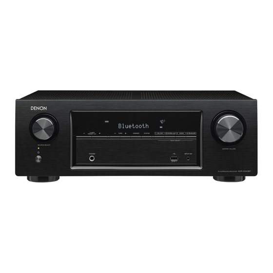
AV SURROUND RECEIVER
AVR-S530BT
AVR-X540BT
• For purposes of improvement, specifications and design are subject to change without notice.
• Please use this service manual with referring to the operating instructions without fail.
• Some illustrations using in this service manual are slightly different from the actual set.
Service Manual
Click here!
On-line service parts list
We are getting ready.
On-line owner's manual
http://manuals.denon.com/AVRS530BT/NA/EN/index.php
http://manuals.denon.com/AVRX540BT/EU/EN/index.php
http://manuals.denon.com/AVRX540BT/AP/ZH/index.php
(You can download PDF owner's manual of "NA" model from SDI server as of March 2017.)
Ver. 1
(Release schedule)
(March 2017)
(April 2017)
Advertisement
Table of Contents
Troubleshooting

Subscribe to Our Youtube Channel
Related Manuals for Denon AVR-S530BT


Summary of Contents for Denon AVR-S530BT
- Page 1 Service Manual Ver. 1 AV SURROUND RECEIVER Click here! AVR-S530BT On-line service parts list AVR-X540BT We are getting ready. On-line owner’s manual (Release schedule) http://manuals.denon.com/AVRS530BT/NA/EN/index.php http://manuals.denon.com/AVRX540BT/EU/EN/index.php (March 2017) http://manuals.denon.com/AVRX540BT/AP/ZH/index.php (April 2017) (You can download PDF owner's manual of "NA" model from SDI server as of March 2017.)
- Page 2 CAUTION IN SERVICING SAFETY PRECAUTIONS NOTE FOR SCHEMATIC DIAGRAM NOTE FOR PARTS LIST INSTRUCTIONS FOR HANDLING SEMICONDUCTORS AND OPTICAL UNIT CAUTION IN SERVICING. Initializing This Unit AVR-S530BT Initializing This Unit AVR-X540BT...
- Page 3 SAFETY PRECAUTIONS ◎ Make a safety check after servicing! The following items should be checked for continued protection of the customer and the service Check that all screws, parts and wires removed or disconnected when servicing have been put back technician.
- Page 4 NOTE FOR SCHEMATIC DIAGRAM WARNING: Parts indicated by the z mark have critical characteristics. Use ONLY replacement parts recommended by the manufacturer. CAUTION: Before returning the set to the customer, be sure to carry out either (1) a leakage current check or (2) a line to chassis resistance check.
- Page 5 CAUTION IN SERVICING. Initializing This Unit AVR-S530BT Initializing This Unit AVR-X540BT Make sure to initialize this unit after replacing the microcomputer or any peripheral equipment, or the Make sure to initialize this unit after replacing the microcomputer or any peripheral equipment, or the digital PCB.
-
Page 6: Schematic Diagrams
ELECTRICAL SCHEMATIC DIAGRAMS LEVEL DIAGRAM SCH01_MCU FRONT ch SCH02_HDMI OSD CENTER ch SCH03_HDMI 4K SURROUND ch SCH04_DSP SUBWOOFER ch SCH05_DIGITAL POWER BLOCK DIAGRAM SCH06_DIR SCH07_AMP ANALOG AUDIO DIAGRAM SCH08_VIDEO, OPTICAL INPUT DIGITAL AUDIO / HDMI DIAGRAM SCH09_USB, BT VIDEO DIAGRAM SCH10_FRONT SCH11_REGULATOR POWER DIAGRAM... - Page 7 SCHEMATIC DIAGRAMS SCH01_MCU CN711 TO FRONT B'D TO BN12B1 FFC WAFER/27P/1.25mm FOR UPDATE MCU PART CN711 FFC 27P CN714 OPEN *EMI Coutermeasure. *EMI Coutermeasure.(C7124/C7125/C7144) MCU+3V3 AGND *EMI Coutermeasure. SUB_MUTE L7103~L7105, L7119: 0 ohm-->600 ohm Bead DGND DAC_MUTE MAIN_VOL_CLK MAIN_VOL_DATA TUNER_INT TUNER_RST *EMI PREPARE(C7149) TUNER_CE...
- Page 8 SCH02_HDMI OSD HDMI OSD PART * HDMI ATC_CEC Connectivity TEST COUNTERMEASURE R7231: OPEN-->0 ohm Change R7231 CEC_COM CEC_5V ADV7623_RST INT_TX INT2_RX INT_RX HDMI_SCL HDMI_SDA TO A4 HDMIOSD_HOLD HDMIOSD_CLK <PVDD_1V8> HDMI_RESET L7209 HDMIOSD_CS 36.7mA CB03YTYH600 INT_TX HDMIOSD_MO <DVDD_1V8> INT2 HDMIOSD_MI L7210 332.4mA INT1 HDMI_SCL...
- Page 9 SCH03_HDMI 4K HDMI 4K PART CEC5V VDD33 L7301 CEC3V3 CB05YTYH221 DGND AVDD33TX L7302 CB05YTYH221 CEC1V1 TO 9A OPEN AVDD33RX0 C7352 OSDTX_2+ AVDD33RX1 L7303 OPEN L7309 OSDTX_2- C7353 CB05YTYH221 OPEN OSDTX_1+ AVDD33RX2 OSDTX_1- C7345 AVDD33RX3 OPEN OSDTX_0+ C7346 OSDTX_0- PVDD33 OPEN OSDTX_C+ L7304 OSDTX_C-...
- Page 10 SCH04_DSP DSP PART DIR_INT CODEC_MUTE DSP_MODE_SEL TO 1B TO 2B DIR_CE DIR_RST DIR_MOSI FROM/TO INPUT/VOLUME PART TO DIGITAL POWER PART DIR_CLK DIR_MISO HDMI_SW DSP_CS DSP_SPC1_IRQ DSP_PCP_BSY DSP_RST DSP_MOSI * Cirrus Recommend DSP_MISO DSP_CLK R7424, R7425: 10K-->3.3K Change. C7442 TO A2 100uF/50V +3V3D C7443...
- Page 11 SCH05_DIGITAL POWER TO A9 TO A7 DIGITAL POWER PART TO HDMI 4K PART TO HDMI OSD PART CN751 CN751 YMW025-06R L7501 1.D5.2V CB03YTYH600 L7502 2.D5.2V TO BN601 R7450 L7508 CB03YTYH600 3.M_RESET L7527 L7503 CB03YTYH600 CB03YTYH600 CB03YTYH600 4.D_GND 5.D_GND R7558 L7429 6.MAIN_POWER CB03YTYH600 Q7521...
- Page 12 SCH06_DIR INPUT/VOLUME PART MCU+3V3 AGND *TUNER MODULE OPTION TU771 SUB_MUTE AVR-S530BT E3 CNVYST990-A9U2 AVR-X540BT E2 CNVYST990-D8E2 DGND CNVYST990-A2J1 AVR-X540BT E1C TU771 DAC_MUTE MAIN_VOL_CLK 1.CH_GND MAIN_VOL_DATA R7637 2.INT TUNER_INT R7651 3./RST TUNER_RST TO A0 R7653 4./CE TUNER_CE R7656 5.SDIO TUNER_SDIO R7657 6.SCLK...
- Page 13 DC RPTECT OPTION ( CEN, SR, SL CH ) 2.0mm 13PIN WIRE OPT. PTC Thermistors BN508 THERMALDET_A FL-CH, SL-CH, CEN_CH *TUNER MODULE OPTION THERMALDET_B FR-CH, SR-CH AVR-S530BT E3 CNVYST990-A9U2 Point A Point B Point C AVR-X540BT E2 CNVYST990-D8E2 Measurement condition BN508 AVR-X540BT E1C...
- Page 14 SCH08_VIDEO, OPTICAL INPUT VIDEO/OPTICAL PART NLM2595 S/W TABLE(SW2,5 CONTROL) FUNC.IN (14) (10) MUTE X (L) R7807 270(1W) MEDIA PLAYER CBL/SAT CN781 R7808 270(1W) C7805 JK781 10/50V CJJ4S010Z CBL/SAT IN 1.+12V J7806 OPEN 2.VGND 3.-12V 4.CVBS_SW2 MEDIA PLAYER IN C7804 5.CVBS_SW5 10/50V 6.+5VD R7801...
- Page 15 SCH09_USB, BT USB / BT PART ( SETUP MIC ) D9014 CDS3C05HDMI1 C9107 OPEN C9029 0.1uF KDS160 D9010 L9022 OPEN JK91 D9011 KDS160 CJJ9X010Z 4.DGND 3.USBD+ C9037 OPEN 2.USBD- 1.VBUS C9030 0.1uF RN909 0 X 2 C9010 220/6.3V OPTION IC905 R9012 2.2K CVIBD82065FVJ-E2...
- Page 16 2. MIC_SIGNAL C1452 C1450 R1076 R1077 R1078 R1079 R1080 50V/10uF R1433 OPTION OPTION OPTION OPTION OPTION 3. -12V KEY2 AVR-S530BT/AVR-X540BT RESISTOR VALUE 4. +12V R1408 SW117 SW118 SW119 KEY_1 KEY_2 KEY_3 C1402 5. MIC_DET R1090 R1083 R1084 R1085 R1071 R1072...
- Page 17 F3004 AC120V OPEN OPEN 932Series 932Series AC230V AVR-S730H/X1400H AC220V 218Series 218Series OPEN OPEN D3101 AC100V OPEN AVR-S530BT/X540BT AC120~230V OPEN OPEN 932Series 932Series IC305 CVIKIA7805BPI FUSE OPTION F3004 IC301 T 1.25A L 250V CVIKIA7812BPI D3001 1N4007 F3002 D3002 1N4007 T 1.25A L 250V BN301 5.DA+5V...
- Page 18 YW396-NNB CMD1A629 BRACKET IC604 TO CN751 AVR-S730H/X1400H CVIPST8448NR_A AC100~120V T 6.3A L 250V AC220~230V T 3.15A L 250V C6029 0.1uF(1608) AVR-S530BT/X540BT AC120V T 5A L 250V R6025 AC220~230V T 2.5A L 250V 4.7K(1608) OPTION C6022 OPEN J6014 OPEN J6015 OPEN...
- Page 19 PRINTED CIRCUIT BOARDS DIGITAL, USB WIRE GUIDE, VIDEO, TUNER, PHONE WIRE GUIDE, FRONT CABLE GUIDE Lead-free Solder When soldering, use the Lead-free Solder (Sn-Ag-Cu). DIGITAL (A SIDE) DIGITAL (B SIDE) MEDIA PLAYER CBL/SAT COAX IN MONITOR BD(4K) CBL/SAT(4K) MEDIA PLAYER DVD/Blu-ray GAME(4K) JK771...
- Page 20 MAIN MAIN (A SIDE) MAIN (A SIDE) D5806...
- Page 21 USB&BT, FRONT, PHONE, STANDBY USB&BT (A SIDE) USB&BT (B SIDE) FRONT (A SIDE) FRONT (B SIDE) C1402 C1406 C9034 CUP12743Z C1411 C1410 C1405 R9062 BN914 C9056 C9013 R9063 D1401 R1412 R1405 MP 2015.02.24 C9021 R9064 IC906 C9027 R9028 R9024 R1411 R1403 C9054 L9013...
- Page 22 Pri. Pri. R6015 D6012 J6018 ZD611 IC601 J6010 CN602 ZD613 CN601 ZD614 C6008 C6013 ZD616 ZD618 AVR-S530BT/X540BT C6001 D6008 IC602 Pri. Pri. T 2.5A L 250V T6001 (AC220V~230V AREA) Sec. J6001 Sec. R6016 D6013 R6034 T 5A L 250V BONDING...
- Page 23 LEVEL DIAGRAM FRONT ch AVR-S530BT / X540BT LEVEL1 DIAGRAM...
- Page 24 CENTER ch AVR-S530BT / X540BT LEVEL2 DIAGRAM...
- Page 25 SURROUND ch AVR-S530BT / X540BT LEVEL3 DIAGRAM...
- Page 26 SUBWOOFER ch AVR-S530BT / X540BT LEVEL4 DIAGRAM...
- Page 27 BLOCK DIAGRAM ANALOG AUDIO DIAGRAM AVR-S530BT / X540BT ANALOG AUDIO DIAGRAM...
- Page 28 DIGITAL AUDIO / HDMI DIAGRAM AVR-S530BT/X540BT DIGITAL AUDIO/HDMI BLOCK DA_FL DIR/CODEC CS42528 DA_FR LRCK DA_CEN SCLK DA_SW CODEC VOLUME DIGITAL SERIAL DIGTAL IN CONTROL FILTER ANALOG DA_SL PORT FILTER OPTICAL IN1 DA_SR OPTICAL IN2 COAXIAL IN1 GAIN DIGITAL & FILTER...
- Page 29 VIDEO DIAGRAM AVR-S530BT / X540BT VIDEO BLOCK...
- Page 30 POWER DIAGRAM AVR-S530BT/X540BT VCC DIAGRAM HI+B MAIN+B LOW+B MAIN-B S1(AMP+B,-B) 178mA RELAY*5 HI-B 25mA VOLUME IC LOW-B (NJU72340A) TFZV7.5B 32mA A+12V (NJM8080 X 4) 45mA BU33TD3WG DA+3.3V (USB DAC:PCM5100) 10mA +5VA (NJM2115MDTE1 X 2) KIA7805BPI S2(+12V,-12V) 50mA TUNER+5V 75mA CS42528(VA)
- Page 31 WIRING DIAGRAM AVR-S530BT/X540BT WIRING DIAGRAM AC CORD DIGITAL PCB CN781 VIDEO PCB SMPS<-AC IN CN771 CN741 CN752 CN711 CN751 CN602 SMPS<-DIGITAL CN772 CN752 CN712 CN601 REGUL.<- DIGITAL REGULATOR PCB SMPS PCB CN503 BN501 BN502 MAIN PCB BN505 TRANS->MAIN CN102 TRANS...
- Page 32 SEMICONDUCTORS Only major semiconductors are shown, general semiconductors etc. are omitted to list. The semiconductor which described a detailed drawing in a schematic diagram are omitted to list. STM32F101xC, STM32F101xD, STM32F101xE Pinouts and pin descriptions 1. IC's Pinouts and pin descriptions STM32F101ZE (DIGITAL : IC711) Pass- Figure 3.
- Page 33 Pass- Pass- Pin Name Symbol Function Pin Name Symbol Function Pullup STBY stop Pullup STBY stop Trough STBY Trough STBY 72 VDD_1 3.3V 126 PG11 EEPROM_SCL EEPROM SCL M3VPu 73 PB12 DA_POWER DA_POWER TIMING control 127 PG12 NC(DAC_MUTE) NC(DAC Mute control) 74 PB13 USB_POWER1 USB_POWER1(1.2V) TIMING control...
- Page 34 ADV7623 Hardware Manual M24128, M24C64, M24C32 Description M24C32WMN6TP (DIGITAL : IC712) Table 6. Function Descriptions Terminal Functions Table 2. Signal names Location Mnemonic Type Description Signal name Function Direction DDCC_SCL Digital Input HDCP slave serial clock port C. DDCC_SCL is a 3.3 V input that is 5 V E0, E1, E2 Chip Enable Input...
- Page 35 ADV7623 Hardware Manual ADV7623 Hardware Manual Location Mnemonic Type Description Location Mnemonic Type Description D in the HDMI interface. TXGND Ground TXAVDD Ground RXD_0+ HDMI Input Digital input channel 0 True of port D in TX0- HDMI Output Differential Output Channel 0 the HDMI interface.
- Page 36 ADV7623 Hardware Manual ADV7623 Hardware Manual Location Mnemonic Type Description Location Mnemonic Type Description MCLK_IN Digital Input Audio Reference Clock. 128 × N × fs with N = 1, 2, 3, or 4. Set to 128 × sampling AP0_OUT Digital Output Audio output port 0.
- Page 37 ADV7623 Hardware Manual ADV7623 Hardware Manual Location Mnemonic Type Description Location Mnemonic Type Description CGND Ground TVDD and CVDD Ground B in the HDMI interface. RXA_C- HDMI Input Digital input clock Complement of port A RXB_1+ HDMI Input Digital input channel 1 true of port B in the in the HDMI interface.
- Page 38 CS497024CVZ (DIGITAL : IC741) MX25L8006EM2I-12G (DIGITAL : IC742) PIN DESCRIPTION SYMBOL DESCRIPTION SO/SIO1 HOLD# Chip Select Serial Data Input (for 1 x I/O)/ Serial Data SCLK SI/SIO0 Input & Output (for Dual Output mode) SI/SIO0 Serial Data Output (for 1 x I/O)/ Serial Data SO/SIO1 Output (for Dual Output mode) Clock Input...
- Page 39 M12L16161A5TG2Q (DIGITAL : IC743) CS42528-CQ (DIGITAL : IC744) Terminal Functions Block diagram Name Input Function System Clock Active on the positive going edge to sample all inputs. Disables or enables device operation by masking or enabling all inputs except Chip Select CLK, CKE and L(U)DQM.
- Page 40 TC74VHC157F/FN/FT/FK TC74VHC157FT (DIGITAL : IC745) Terminal Functions Pin Assignment IEC Logic Symbol (15) SELECT SELECT A S G 1 MUX (11) (10) (14) (12) (13) (top view) Truth Table Inputs Output SELECT X: Don’t care TPS563200 (DIGITAL : IC751 - IC753) TPS562200, TPS563200 DDC (SOT) Package Top View...
- Page 41 NJU72340A (DIGITAL : IC761) BX8804 (USB : IC901) TDO / GP44 GP05 / SPI0 CK TMS / GP45 GP04 / SPI0 CS GP03 / EXT Clock GP29 / CDDSP SCOR0 ECSN GP30 / CDDSP BCLK0 EOEN / GP42 GP31 / CDDSP DATA0 EWEN / GP41 GP32 / CDDSP LRCK0 EAD20 / GP40 / Boot Mode...
- Page 42 Terminal Functions External SDRAM Bank selector 1 External program address bus [14] LDQM SDRAM Lower byte data mask External program address bus [15] Name Type Description Alternative Function UDQM SDRAM Upper byte data mask External program address bus [16] ADIN1 ADC analog input[1] SDCSN SDRAM Chip select...
- Page 43 GP19 General Purpose IO 19 SPI1 MISO GP20 General Purpose IO 20 SPI1 MOSI External Interrupt 3 GP21 General Purpose IO 21 SPI2 CS GP30 General Purpose IO 30 CDDSP BCLK0 DDATA Audio serial data for external DAC GP31 General Purpose IO 31 CDDSP DATA0 IOVDD33 I/O Power supply (3.3V)
- Page 44 W9864G6KH-6 (USB : IC902) MX25L1606EM2I-12G (USB : IC904) Terminal Functions Terminal Functions BD82065FVJ (USB : IC905)
- Page 45 TOP268VG (SMPS : IC601) DRAIN (D) CONTROL (C) INTERNAL SUPPLY SHUNT REGULATOR/ ERROR AMPLIFIER SOFT START 5.8 V 4.8 V 5.8 V INTERNAL UV PS(UPPER) COMPARATOR V I (LIMIT) CURRENT LIMIT ADJUST ÷ 16 PS(LOWER) ON/OFF SHUTDOWN/ EXTERNAL CURRENT AUTO-RESTART CURRENT LIMIT LIMIT (X) COMPARATOR...
- Page 46 ANODE CONNECTION 2. FL DISPLAY 17G(AD3) 18G(AD4) FLD (018BT021GINK) (FRONT : FL101) 8G 9G 10G 11G 12G 13G 14G 15G 16G PIN CONNECTION NOTE 1) F1, F2 ----Filament 2) NP ------No pin 3) DL ------Datum Line 4) NX ------No extend pin 5) LGND ----Logic GND pin 6) PGND ----Power GND pin 7) VH...
- Page 47 MECHANICAL DISASSEMBLY Flowchart 1. FRONT PANEL ASSY 2. VIDEO PCB 3. DIGITAL PCB 4. MAIN PCB 5. SMPS PCB 6. REGULATOR PCB 7. TRANS EXPLODED VIEW PACKING VIEW...
- Page 48 DISASSEMBLY Flowchart • Remove each part following the flow below. • Reassemble the removed parts in the reverse order. • Read "SAFETY PRECAUTIONS" before reassembling the removed parts. • If wire bundles are removed or moved during adjustment or part replacement, reshape the wires after completing the work. Failure to shape the wires correctly may cause problems such as noise. •...
- Page 49 • The photographs with no shooting direction indicated were taken from the top of the unit. (1) Remove the screws. • Photos of AVR-S530BT E3 are used in this manual. The viewpoint of each photograph (Shooting direction : X) [View from the top] ↓Shooting direction: B↓...
- Page 50 2. VIDEO PCB 3. DIGITAL PCB Proceeding : TOP COVER → VIDEO PCB Proceeding : TOP COVER → VIDEO PCB → DIGITAL PCB (1) Remove the screws. Remove the FFC. (1) Remove the screws. Remove the connector. Remove the FFC. CN712 CN772 CN713...
- Page 51 4. MAIN PCB 5. SMPS PCB Proceeding : TOP COVER → VIDEO PCB → DIGITAL PCB → MAIN PCB Proceeding : TOP COVER → SMPS PCB (1) Remove the screws. "EXPLODED VIEW" for instructions on removing the SMPS PCB. 6. REGULATOR PCB Proceeding : TOP COVER →...
- Page 52 EXPLODED VIEW Please see the last chapter for the part list. AVRS530BT/X540BT EXPLODED VIEW S6 x2 S3 x2 S6 x1 S3 x1 S6 x3 S3 x6 S3 x1 S9 x3 S6 x7 S6 x4 S3 x2 S6 x3 S6 x1 S7 x2 S9 x3 S4 x1...
- Page 53 PACKING VIEW Please see the last chapter for the part list. 5-10 UK plug Adaptor...
- Page 54 5. Bluetooth / USB 6. SMPS CLOCK FLOW & WAVE FORM IN DIGITAL BLOCK SPECIAL MODE Special mode setting button AVR-S530BT Special mode setting button AVR-X540BT 1. Version Display Mode 2. Video Format and Display Language change mode 3. Product mode 3-1.
- Page 55 TROUBLE SHOOTING 1. POWER 1.1. The unit does not power on 1.2. Fuse is blown The unit does not power on Blown fuse Does the power indicator on the front panel flash Does the power indicator on the front panel Check for short circuits between the Check the rectifier diode in the in green when the power is turned on?
- Page 56 2. Analog video MONITOR OUT (CVBS) output NG Is the power voltage being output correctly? : [C7810 : + side] The power supply circuit is faulty. : [C7811 : - side] Check the pattern between [JK781] and [IC781], Is a signal being output from the video ampli- Does the signal input to the video amplifier? and then check the Blu-ray/DVD player or the fier?
- Page 57 3.1. No picture or sound is output (HDMI to HDMI) No picture or sound is output. (8) When using a DENON Blu-ray/DVD player, is the "HDMI" indicator of the fluorescent display lit? Proceed to YES when using a Blu-ray/DVD player produced by other manufactures.
- Page 58 When the Blu-ray/DVD player is connected, check the voltage of the HDMI connector input on (18) the side that the Blu-ray/DVD player is connected to. When using a DENON Blu-ray/DVD player, is the The pattern and circuit from HDMI connector [JK721- Check the waveform of DDC_CLK/DDC_DATA "HDMI"...
- Page 59 3.2. HDMI test point and waveforms DDC_CLK/DDC_DATA/TMDS : Check items (17),(19) COAX IN MEDIA PLAYER CBL/SAT MONITOR BD(4K) CBL/SAT(4K) MEDIA PLAYER DVD/Blu-ray GAME(4K) JK771 R7627 C7702 C7703 R7738 R7765 R7655 T7325 T7208 C7621 R7764 JK726 JK725 JK724 JK723 JK722 JK721 JK784 C7622 D7326...
- Page 60 4. AUDIO 4.1. AUDIO CHECK No audio output CHECK 1 INPUT SURROUND MODE SOURCE Check the ANALOG AUDIO BLOCK Audio output OK? ANALOG 2CH DIRECT ANALOG CHECK 2 INPUT SURROUND MODE SOURCE Check the DIGITAL AUDIO BLOCK Legacy Audio output OK? COAX or OPT (PCM or DolbyDigital or dts…) CHECK 3...
- Page 61 4.2. Power AMP (MAIN PCB) No audio output. Protection is activated. Is the power transistor open or short circuited? Replace the power transistor. 2SB1560 / 2SD2390 Is the emitter resistor of the power transistor open? Replace the emitter resistor. 0.47 Ω Is the base resistor of the power transistor open? Replace the base resistor.
- Page 62 5. Bluetooth / USB 5.1. Cannot establish a Bluetooth connection 5.2. Cannot recognize the connected USB device Check the Bluetooth device being used Check the USB device being used Are there other Bluetooth devices on close by? Turn off other Bluetooth devices. Is a USB hub being used? Do not use a USB hub.
- Page 63 6. SMPS Operation waveform for each part DC 5V is not output. Primary drain After primary side rectification *OPTION (Caution: High voltage, electric shock) (Caution: High voltage, electric shock) C6002 250V/0.01uF *OPTION Replace the [IC601 : TOP268VG D6001 1N4007 Is [IC601 : TOP268VG] damaged? and D6001, D6002, D6003, D6002 1N4007 After secondary rectifications...
- Page 64 CLOCK FLOW & WAVE FORM IN DIGITAL BLOCK WAVE FORM IC721 ADV7623BSDZ HDMI Transceiver (W/GUI) IC731 MN864788 CH1:RXP2 HDMI 1 - 2 HDMI 3 - 5 IC744 CS42528 (DIR+CODEC) RMCK(55) Coaxial1 (49)RXP0 (43)RXP6/GPO6 Optical1 SAI_SCLK(61) (32)DAI2_LRCK IC741 (47)RXP2/GPO2 Optical2 SAI_LRCK(60) (33)DAI2_SCLK CS497024CVZ (34)DAI2_DATA,DSD5...
- Page 65 SPECIAL MODE Special mode setting button AVR-S530BT b No. 1, 2 : While holding down buttons "A" and "B" simultaneously, press the power button to turn on the power. b No. 3, 4 : While the power is on, hold down buttons "A", "B", and "C" for at least 3 seconds .
- Page 66 Special mode setting button AVR-X540BT b No. 1, 2 : While holding down buttons "A" and "B" simultaneously, press the power button to turn on the power. b No. 3, 4 : While the power is on, hold down buttons "A", "B", and "C" for at least 3 seconds . Mode Button A Button B...
- Page 67 Version information is displayed when the device is started in this mode. See the table below for descriptions of the displayed errors and countermeasures for these. If multiple errors occur, only one item is displayed. 1.2. Starting up AVR-S530BT States Display Condition ·...
- Page 68 AVR-X540BT : "TUNER PRESET CH+" or "DIMMER" Lang.:<CHINESE> · AVR-S530BT : Press the "TUNER PRESET -" button to confirm the displayed mode. · AVR-X540BT : Press the "TUNE -" button to confirm the displayed mode. Do not turn off the power until the display switches to the normal mode screen.
- Page 69 TUNER:AM**/FM*** REMOTE LOCK:On AVR-S530BT : "TUNE +" AVR-X540BT : "STATUS" AVR-S530BT : Enter using the "TUNER PRESET CH-" button. AVR-X540BT : Enter using the "TUNE -" button. OSD Update:Off AVR-S530BT : "TUNE +" The display then returns to normal mode.
- Page 70 AVR-S530BT : "TUNER PRESET CH+" or "TUNE -" AVR-X540BT : "TUNER PRESET CH+" or "DIMMER" TUNER:AM10/FM200 AVR-S530BT : Enter using the "TUNER PRESET CH-" button. AVR-X540BT : Enter using the "TUNE -" button. The display then returns to normal mode.
- Page 71 · The protection history can be checked. PRT:DC (a) If no protections has occurred. AVR-S530BT : Press and hold the "TUNER PRESET CH-" button for 3 seconds. NO PROTECT AVR-X540BT : Press and hold the "TUNE -" button for 3 seconds.
- Page 72 3-5. Mic Mode This is not used during servicing. Do not use. 3-3.1. Operations Exit the Mic Mode Remove the power plug to exit this mode. MIC Mode...
-
Page 73: Adjustment Procedure
ADJUSTMENT Adjusting Idling Current 1. Preparation MAIN PCB (1) Prepare a DC voltmeter. (2) Place the unit under normal usage conditions, away from highly ventilated areas such as next to an air conditioning machine or electric fan. DC Voltmeter The set requires an ambient temperature of 15℃ to 30℃ and standard humidity. (3) Settings of This Unit •... - Page 74 UPDATING PROCEDURE AFTER REPLACING THE PCB. PROCEDURE AFTER REPLACING THE U-COM, ETC. FIRMWARE UPDATE PROCEDURE 1. Items necessary for update 2. Update preparation with a USB flash drive...
- Page 75 PROCEDURE AFTER REPLACING THE PCB. PROCEDURE AFTER REPLACING THE U-COM, ETC. The procedure after replacing the printed circuit boards is as follows. The procedure after replacing the u-COM (microprocessor), flash ROM, etc. is as follows. (1) Change the resistor for setting the region. Implement the update method when the DIGITAL PCB or network module is replaced.
- Page 76 FIRMWARE UPDATE PROCEDURE 1. Items necessary for update Items necessary for update are as follows. Offered / not Offered Update Type Needed Part for Update Requirement Standard Service Equipment Purchase from D&M Article code Download from SDI Not offered by D&M 2.
- Page 77 2. Update preparation with a USB flash drive 2.3. Insert the USB memory into the USB port. You can update the firmware by downloading the latest version with USB flash drive. 2.1. Connecting to the USB flash drive (1) Preparation ・...
-
Page 78: Update Time
2.4. Start the update. (3) Press the "ENTER" button. Turn on the power of this unit. Press the "SETUP" button on the remote control. (1) Select "General". Firmware :Start General (4) Select "Yes". Press "ENTER" button. (2) Select "Firmware". Firmware :Yesr- Firmware Update Time**:**... - Page 79 2.5. About the error codes No FirmwareFile in USB. FirmwareFile in USB for unsupported Model name/area...
- Page 80 www.denon.com...
- Page 81 USB PCB ASS'Y ※Parts indicated by "nsp"on this table cannot be supplied. Part indicated by "@" mark is not illustrated in the exploded view. ※The parts listed below are only for maintenance. Therefore they might differ from the parts used in the unit in appearances or dimensions. NOTE:The symbols in the column Remarks indicate the following destinations.
- Page 82 REF No. Part No. Part Name Remarks Q'ty C1403 CAP, CHIP(1608, 50V/100pF, C0G)_SAMSUNG CCUS1H101JAS C1405 CAP,ALUMINUM ELECTROLYTIC (16V/10uF) CCEC1CMVG100T C1406 CAP, CHIP(1005, 16V/0.1uF, X7R)_SAMSUNG CCUI1C104KCS C1407 CAP,ALUMINUM ELECTROLYTIC CAPACITORS(16V/100uF) CCEC1CMVG101T C1408 CAP, CHIP(1608, 50V/27pF, C0G)_SAMSUNG CCUS1H270JAS C1410 CAP,ALUMINUM ELECTROLYTIC (16V/10uF) CCEC1CMVG100T C1411 CAP,ALUMINUM ELECTROLYTIC (16V/10uF)
- Page 83 REF No. Part No. Part Name Remarks Q'ty CN911 WAFER , CARD CABLE (SMD, 09P-1mm, ANGLE, H : 2mm) CJP10GB310ZY JK105 943643102930S JACK, STEREO, 3.5mm MINI, BLACK MOLD CJJ2D029Z JK91 943643101590S JACK, USB STRAIGHT(BLACK 1.5A) CJJ9X010Z L1401 FERRITE CHIP BEAD(1608/60R,CB03YTYH600) CLZ9R005V L9010 FERRITE CHIP BEAD(2012/220R, CB05YTYH221)
- Page 84 FRONT FRONT PCB ASS'Y ※Parts indicated by "nsp"on this table cannot be supplied. Part indicated by "@" mark is not illustrated in the exploded view. ※The parts listed below are only for maintenance. Therefore they might differ from the parts used in the unit in appearances or dimensions. NOTE:The symbols in the column Remarks indicate the following destinations.
- Page 85 FRONT REF No. Part No. Part Name Remarks Q'ty C1072 CAP, CHIP(1608, 50V/680pF, C0G)_SAMSUNG CCUS1H681JAS C1073 CAP, CHIP(1608, 50V/0.1uF, X7R)_SAMSUNG CCUS1H104KCS C1076 CAP, CHIP(1608, 50V/0.01uF, X7R)_SAMSUNG CCUS1H103KCS C1077 CAP, CHIP(1608, 50V/0.01uF, X7R)_SAMSUNG CCUS1H103KCS C1081 CAP, CHIP(1608, 50V/0.1uF, X7R)_SAMSUNG CCUS1H104KCS C1424 CAP, CHIP(1608, 50V/0.1uF, X7R)_SAMSUNG CCUS1H104KCS C1425...
- Page 86 MAIN MAIN PCB ASS'Y ※Parts indicated by "nsp"on this table cannot be supplied. Part indicated by "@" mark is not illustrated in the exploded view. ※The parts listed below are only for maintenance. Therefore they might differ from the parts used in the unit in appearances or dimensions. NOTE:The symbols in the column Remarks indicate the following destinations.
- Page 87 MAIN REF No. Part No. Part Name Remarks Q'ty R5218 RES, M-OXIDE FILM(1W/4.7ohm) CRG1SANJ4R7RT R5219 943124500050S RES, M-OXIDE FILM(2W/0.47ohm) CRG2SANJR47RT R5220 943124500050S RES, M-OXIDE FILM(2W/0.47ohm) CRG2SANJR47RT R5221 943124500050S RES, M-OXIDE FILM(2W/0.47ohm) CRG2SANJR47RT R5222 943124500050S RES, M-OXIDE FILM(2W/0.47ohm) CRG2SANJR47RT R5223 RES, CARBON(1/5W,470Kohm,J) CRD20TJ474T R5224 RES, CARBON(1/5W,270Kohm,J)
- Page 88 MAIN REF No. Part No. Part Name Remarks Q'ty R5727 RES, M-OXIDE FILM(2W/470ohm) CRG2SANJ471RT R5728 RES, CHIP(1608/5%/0ohm) CRJ10DJ0R0T R5817 RES, CARBON(1/5W,33Kohm,J) CRD20TJ333T R5818 RES, CARBON(1/5W,33Kohm,J) CRD20TJ333T R5819 RES, CARBON(1/5W,33Kohm,J) CRD20TJ333T R7801 RES, CHIP(1608/5%/1.8Kohm) CRJ10DJ182T R7802 RES, CHIP(1608/1%/82ohm) CRJ10DF82R0T R7803 RES, CHIP(1608/1%/75ohm) CRJ10DF75R0T R7804 RES, CHIP(1608/1%/75ohm)
- Page 89 MAIN REF No. Part No. Part Name Remarks Q'ty JK782 943262100150S MODULE , OPTICAL(RX 16MHz) CJSJSR1124 JK783 943262100150S MODULE , OPTICAL(RX 16MHz) CJSJSR1124 L5101 943115100310S COIL , SPEAKER ( 0.5UH ) CLEY0R5KAD L5201 943115100310S COIL , SPEAKER ( 0.5UH ) CLEY0R5KAD L5301 943115100310S...
- Page 90 POWER POWER PCB ASS'Y ※Parts indicated by "nsp"on this table cannot be supplied. Part indicated by "@" mark is not illustrated in the exploded view. ※The parts listed below are only for maintenance. Therefore they might differ from the parts used in the unit in appearances or dimensions. NOTE:The symbols in the column Remarks indicate the following destinations.
- Page 91 POWER REF No. Part No. Part Name Remarks Q'ty ! CY602 943132100800S CAP, CERAMIC(X1/Y1, 470pF, AC400V) CCKDCT471KB ! F3003 943652500510D FUSE(932Series, 250V/1.25A) CBA2J1250TLEBT ! F3004 943652500510D FUSE(932Series, 250V/1.25A) CBA2J1250TLEBT ! F6001 963652010510S FUSE(S506 Series, 250V,2A) CBA2C2000TLEC ! F6001 963652010500S FUSE(S506 Series, 250V,1.6A) E2,E1C CBA2C1600TLEC F6001...
- Page 92 DIGITAL DIGITAL PCB ASS'Y ※Parts indicated by "nsp"on this table cannot be supplied. Part indicated by "@" mark is not illustrated in the exploded view. ※The parts listed below are only for maintenance. Therefore they might differ from the parts used in the unit in appearances or dimensions. NOTE:The symbols in the column Remarks indicate the following destinations.
- Page 93 DIGITAL REF No. Part No. Part Name Remarks Q'ty R7165 RES, CHIP(1005/5%/100ohm) CRJ06IJ101T R7166 RES, CHIP(1608/5%/2.2Kohm) CRJ10DJ222T R7167 RES, CHIP(1005/5%/100Kohm) CRJ06IJ104T R7168 RES, CHIP(1608/5%/33Kohm) CRJ10DJ333T R7170 RES, CHIP(1005/5%/0ohm) CRJ06IJ0R0T R7171 RES, CHIP(1005/5%/100ohm) CRJ06IJ101T R7172 RES, CHIP(1005/5%/0ohm) CRJ06IJ0R0T R7173 RES, CHIP(1005/5%/33ohm) CRJ06IJ330T R7174 RES, CHIP(1005/5%/33ohm)
- Page 94 DIGITAL REF No. Part No. Part Name Remarks Q'ty R7314 RES, CHIP(1005/5%/47Kohm) CRJ06IJ473T R7315 RES, CHIP(1005/5%/47Kohm) CRJ06IJ473T R7316 RES, CHIP(1005/5%/0ohm) CRJ06IJ0R0T R7317 RES, CHIP(1005/5%/0ohm) CRJ06IJ0R0T R7318 RES, CHIP(1005/5%/0ohm) CRJ06IJ0R0T R7325 RES, CHIP(1005/5%/10Kohm) CRJ06IJ103T R7333 RES, CHIP(1005/5%/33ohm) CRJ06IJ330T R7334 RES, CHIP(1005/5%/33ohm) CRJ06IJ330T R7335 RES, CHIP(1005/5%/33ohm)
- Page 95 DIGITAL REF No. Part No. Part Name Remarks Q'ty R7547 RES, CHIP(1005/5%/47Kohm) CRJ06IJ473T R7550 RES, CHIP(1005/5%/10Kohm) CRJ06IJ103T R7551 RES, CHIP(1005/5%/3.3Kohm) CRJ06IJ332T R7552 RES, CHIP(1608/5%/0ohm) CRJ10DJ0R0T R7553 RES, CHIP(1005/5%/10Kohm) CRJ06IJ103T R7554 RES, CHIP(1005/5%/33Kohm) CRJ06IJ333T R7555 RES, CHIP(1005/5%/10Kohm) CRJ06IJ103T R7556 RES, CHIP(1005/5%/10Kohm) CRJ06IJ103T R7557 RES, CHIP(1005/5%/10Kohm)
- Page 96 DIGITAL REF No. Part No. Part Name Remarks Q'ty R7756 RES, CHIP(1608/5%/100ohm) CRJ10DJ101T R7757 RES, CHIP(1608/5%/12Kohm) CRJ10DJ123T R7758 RES, CHIP(1608/5%/10Kohm) CRJ10DJ103T R7762 RES, CHIP(1005/5%/0ohm) CRJ06IJ0R0T R7763 RES, CHIP(1005/5%/0ohm) CRJ06IJ0R0T R7774 RES, CHIP(1608/5%/0ohm) CRJ10DJ0R0T R7775 RES, CHIP(1608/5%/0ohm) CRJ10DJ0R0T R7776 RES, CHIP(1608/5%/0ohm) CRJ10DJ0R0T R7777 RES, CHIP(1608/5%/0ohm)
- Page 97 DIGITAL REF No. Part No. Part Name Remarks Q'ty C7304 CAP, CHIP(1608, 50V/0.1uF, X7R)_SAMSUNG CCUS1H104KCS C7305 CAP, CHIP(1608, 50V/0.1uF, X7R)_SAMSUNG CCUS1H104KCS C7306 CAP, CHIP(1005, 16V/0.1uF, X7R)_SAMSUNG CCUI1C104KCS C7307 CAP, CHIP(1608, 50V/0.1uF, X7R)_SAMSUNG CCUS1H104KCS C7308 CAP, CHIP(1005, 16V/0.1uF, X7R)_SAMSUNG CCUI1C104KCS C7309 CAP, CHIP(1608, 50V/0.1uF, X7R)_SAMSUNG CCUS1H104KCS C7310...
- Page 98 DIGITAL REF No. Part No. Part Name Remarks Q'ty C7468 CAP, ELECT(10V/100uF) CCEA1AH101T C7469 CAP, CHIP(1005, 16V/0.1uF, X7R)_SAMSUNG CCUI1C104KCS C7470 CAP, ELECT(10V/100uF) CCEA1AH101T C7471 CAP, CHIP(1005, 16V/0.1uF, X7R)_SAMSUNG CCUI1C104KCS C7473 CAP, CHIP(1005, 16V/0.1uF, X7R)_SAMSUNG CCUI1C104KCS C7477 CAP, CHIP(1005, 16V/0.1uF, X7R)_SAMSUNG CCUI1C104KCS C7478 CAP, CHIP(1005, 16V/0.1uF, X7R)_SAMSUNG...
- Page 99 DIGITAL REF No. Part No. Part Name Remarks Q'ty C7657 CAP, CHIP(1608, 50V/330pF, C0G)_SAMSUNG CCUS1H331JAS C7658 CAP, CHIP(1608, 50V/1500pF , X7R)_SAMSUNG CCUS1H152KCS C7659 CAP, CHIP(1608, 50V/1500pF , X7R)_SAMSUNG CCUS1H152KCS C7660 CAP, CHIP(1005, 16V/0.1uF, X7R)_SAMSUNG CCUI1C104KCS C7661 CAP, CHIP(1608, 50V/330pF, C0G)_SAMSUNG CCUS1H331JAS C7662 CAP, CHIP(1608, 50V/330pF, C0G)_SAMSUNG...
- Page 100 DIGITAL REF No. Part No. Part Name Remarks Q'ty L7306 FERRITE CHIP BEAD(2012/220R, CB05YTYH221) CLZ9R018V L7308 FERRITE CHIP BEAD(2012/220R, CB05YTYH221) CLZ9R018V L7309 FERRITE CHIP BEAD(2012/220R, CB05YTYH221) CLZ9R018V L7310 FERRITE CHIP BEAD(2012/220R, CB05YTYH221) CLZ9R018V L7401 FERRITE CHIP BEAD(2012/220R, CB05YTYH221) CLZ9R018V L7402 FERRITE CHIP BEAD(2012/220R, CB05YTYH221) CLZ9R018V L7404...
- Page 101 VGW1A553EA 943402106420S FRONT/SUB PANEL ASS'Y E2,E1C VGW1A553DA 943416101490D WINDOW , FL VGU1A462M 943416101320D WINDOW E2,E1C VGU1A462N 42141002400AD BADGE , DENON CGB1A254Z-V1 943411101750D BUTTON , POWER CBT1A1167 943423100510D INDICATOR , POWER CGL1A299A36 943411103220D BUTTON , SOURCE VBT1A1195 943411103210D BUTTON , NETWORK...
- Page 102 PACKING PACKING ※Parts indicated by "nsp"on this table cannot be supplied. Part indicated by "@" mark is not illustrated in the exploded view. ※The parts listed below are only for maintenance. Therefore they might differ from the parts used in the unit in appearances or dimensions. NOTE:The symbols in the column Remarks indicate the following destinations.
Need help?
Do you have a question about the AVR-S530BT and is the answer not in the manual?
Questions and answers