Table of Contents
Advertisement
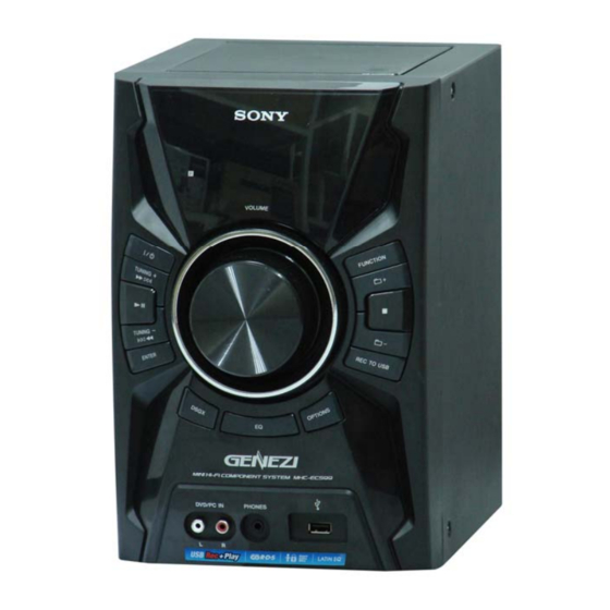
SERVICE MANUAL
Ver. 1.0 2012.02
• HCD-EC599 is the amplifi er, USB, CD player
and tuner section in MHC-EC599.
• "WALKMAN" and "WALKMAN" logo are registered trademarks of Sony Corporation.
• MPEG Layer-3 audio coding technology and patents licensed from Fraunhofer IIS and Thomson.
• MPEG Layer-3 audio coding technology and patents licensed from Fraunhofer IIS and Thomson.
• Windows Media is either a registered trademark or trademark of Microsoft Corporation in the
• Windows Media is either a registered trademark or trademark of Microsoft Corporation in the
United States and/or other countries.
• This product is protected by certain intellectual property rights of Microsoft Corporation. Use or
United States and/or other countries.
• This product contains technology subject to certain intellectual property rights of Microsoft.
distribution of such technology outside of this product is prohibited without a license from Micro-
soft or an authorized Microsoft subsidiary.
Use or distribution of this technology outside of this product is prohibited without the appropriate
license(s) from Microsoft.
Amplifi er section
Argentina model
The following are measured at AC 220 V,
50/60 Hz
Power output (rated):
30 W + 30 W (at 6 ohms, 1 kHz,
1% THD)
Other models
The following are measured at
Mexican model:
AC 127 V, 60 Hz
Other models:
AC 120 V, 220 V, 240 V, 50/60 Hz
Power output (rated):
30 W + 30 W (at 6 ohms, 1 kHz,
1% THD)
RMS output power (reference):
60 W + 60 W (per channel at 6 ohms,
1 kHz)
Inputs
DVD/PC IN L/R
Voltage 1.5 V, impedance 47 kilohms
(USB) port: Type A
Outputs
PHONES (stereo mini jack)
Accepts headphones with an
impedance of 8 ohms or more
9-890-594-01
Sony Corporation
2012B08-1
©
2012.02
Published by Sony EMCS (Malaysia) PG Tec
HCD-EC599
SPECIFICATIONS
USB section
Supported bit rate
MP3 (MPEG 1 Audio Layer-3):
32 kbps – 320 kbps, VBR
WMA: 48 kbps – 192 kbps
AAC: 48 kbps – 320 kbps
Sampling frequencies
MP3 (MPEG 1 Audio Layer-3):
32/44.1/48 kHz
WMA: 44.1 kHz
AAC: 44.1 kHz
Supported USB device
Mass Storage Class
Maximum current
500 mA
Disc player section
System
Compact disc and digital audio system
Laser Diode Properties
Emission Duration: Continuous
Laser Output*: Less than 44.6 μW
* This output is the value measurement
at a distance of 200 mm from the
objective lens surface on the Optical
Pick-up Block with 7 mm aperture.
Frequency response
20 Hz – 20 kHz
Signal-to-noise ratio
More than 90 dB
Dynamic range
More than 88 dB
Model Name Using Similar Mechanism
Base Unit Name
Optical Pick-up Block Name
Tuner section
FM stereo, FM/AM superheterodyne tuner
Antenna
FM lead antenna
AM loop antenna
FM tuner section
Tuning range
87.5 MHz – 108.0 MHz (50 kHz step)
AM tuner section
Tuning range
530 kHz – 1,710 kHz (10 kHz step)
531 kHz – 1,710 kHz (9 kHz step)
Design and specifi cations are subject to
change without notice.
Standby power consumption: 0.5 W
COMPACT DISC RECEIVER
E Model
HCD-EX600
BU-D1BD76
DA11MMVGP
Advertisement
Table of Contents

Related Manuals for Sony HCD-EC599


Summary of Contents for Sony HCD-EC599
- Page 1 • HCD-EC599 is the amplifi er, USB, CD player and tuner section in MHC-EC599. • MPEG Layer-3 audio coding technology and patents licensed from Fraunhofer IIS and Thomson. • “WALKMAN” and “WALKMAN” logo are registered trademarks of Sony Corporation. Model Name Using Similar Mechanism HCD-EX600 •...
-
Page 2: Table Of Contents
COMPONENTS IDENTIFIED BY MARK 0 OR DOTTED LINE WITH MARK 0 ON THE SCHEMATIC DIAGRAMS AND IN THE PARTS LIST ARE CRITICAL TO SAFE OPERATION. REPLACE THESE COMPONENTS WITH SONY PARTS WHOSE PART NUMBERS APPEAR AS SHOWN IN THIS MANUAL OR IN SUPPLEMENTS PUBLISHED BY SONY. -
Page 3: Servicing Notes
HCD-EC599 SECTION 1 SERVICING NOTES LASER DIODE AND FOCUS SEARCH OPERATION NOTES ON HANDLING THE OPTICAL PICK-UP CHECK BLOCK OR BASE UNIT During normal operation of the equipment, emission of the laser diode is prohibited unless the upper lid is closed while turning on The laser diode in the optical pick-up block may suffer electro- the SW305 (push switch type). - Page 4 HCD-EC599 MODEL IDENTIFICATION Distinguish the destination by referring to the model number label or the model number plate or the sculpture of back panel . Argentina and Mexican models MODEL NUMBER LABEL Argentina model Mexican model 4-413-837-0s AR2 4-413-838-0s MX4...
- Page 5 HCD-EC599 TRANS BOARD SERVICE POSITION • SIDE PANEL (R) was removed. TRANS board BD76 BOARD SERVICE POSITION • SIDE PANEL (L) and (R) are removed, and the set is laid. top panel block BD76 board...
-
Page 6: Disassembly
HCD-EC599 SECTION 2 DISASSEMBLY • This set can be disassembled in the order shown below. 2-1. DISASSEMBLY FLOW 2-2. SIDE PANEL (L)/(R) (Page 6) 2-3. TOP PANEL ASSY (Page 7) 2-4. FRONT PANEL BLOCK 2-6. POWER BOARD 2-7. BASE UNIT (BU-D1BD76) -
Page 7: Top Panel Assy
HCD-EC599 2-3. TOP PANEL ASSY top panel assy Lift up the side of the top panel assy in the back and remove the two claws in front of the top panel assy. two claws 3 connector (SW305) flexible flat cable... -
Page 8: Knob (Volume)
HCD-EC599 2-5. KNOB (VOLUME) Note: This illustration sees the front panel block from PANEL board side. front panel block 2 knob (VOLUME) hole PANEL board 1 Push the knob (VOLUME) by flat-head screwdriver. 2-6. POWER BOARD 2 two screws +BV3 (3-CR) -
Page 9: Base Unit (Bu-D1Bd76)
HCD-EC599 2-7. BASE UNIT (BU-D1BD76) Note 1: This illustration sees the top panel assy from base unit side. 4 two insulators (blue) 1 four floating screws (+PTPWHM 2.6) 7 base unit 3 two insulators (BU-D1BD76) (gray) 5 four claws Note 2: Four claws might be fixed by bond. -
Page 10: Test Mode
HCD-EC599 SECTION 3 TEST MODE 3. To release from this mode, press [ ] button. COLD RESET 4. The cold reset is enforced at the same time. The cold reset clears all data including preset data stored in the memory to initial conditions. Execute this mode when returning TUNER STEP CHANGE the set to the customer. - Page 11 HCD-EC599 3. Press three buttons of [u], [ ] and [ ] simultaneously. PROTECT KIND CHECK TEST MODE 4. It enters the CD factory mode and the message “FACTORY” is This mode is used to check types of protect occurred during displayed.
-
Page 12: Electrical Checks
HCD-EC599 SECTION 4 ELECTRICAL CHECKS CD SECTION 0 dB = 1 V TUNER SECTION Note: FM AUTO STOP CHECK 1. CD Block is basically constructed to operate without adjustment. signal 2. Use YEDS-18 disc (Part No. 3-702-101-01) unless otherwise indicat- generator 3. -
Page 13: Diagrams
HCD-EC599 SECTION 5 DIAGRAMS 5-1. BLOCK DIAGRAM – CD/USB Section – OPTICAL PICK-UP BLOCK (DA11MMVGP) 5 AIN MAIN 7 BIN Section LCHO CD/USB-L 6 CIN (Page 14) 8 DIN RCHO R-ch AUTOMATIC POWER 18 LDD CD-MP3 PROCESSOR CONTROL IC101 Q201... -
Page 14: Block Diagram - Main Section
HCD-EC599 5-2. BLOCK DIAGRAM – MAIN Section – J380 PHONES INPUT SELECTOR POWER AMP IC500 IC701 CD/USB Section CD/USB-L CD/USB-L TB701 (Page 13) R-ch 31 CD/USB-R OUT-L LCH IN RCH OUT- OUT-R RCH IN LCH OUT- SPEAKERS J500 IMPEDANCE: USE 6 –... -
Page 15: Block Diagram - Display/Power Section
HCD-EC599 5-3. BLOCK DIAGRAM – DISPLAY/POWER Section – SYSTEM CONTROL IC100 (3/3) SEG0 VSTANDBY LCD100 T601 LIQUID SEG32 POWER CRYSTAL TRANSFORMER VDD1(+3.3V) DISPLAY PANEL COM3 D302 +3.3V COM0 AD +3.3V Q231 SWITCH +4V REG O-AD-SWITCH Q131 IC300 RY651 AC IN D100 VDD3 (+3.3V) - Page 16 HCD-EC599 THIS NOTE IS COMMON FOR PRINTED WIRING BOARDS AND SCHEMATIC DIAGRAMS. • Circuit Boards Location (In addition to this, the necessary note is printed in each block.) For Printed Wiring Boards. For Schematic Diagrams. DB76 board Note: Note: TUNER1 board •...
-
Page 17: Printed Wiring Board - Bd76 Board
HCD-EC599 • 5-4. PRINTED WIRING BOARD – BD76 BOARD – • See page 16 for Circuit Boards Location. : Uses unleaded solder. BD76 BOARD (Component Side) BD76 BOARD (Conductor Side) R305 R304 C302 R301 R302 IC301 M401 (SPINDLE) C301 CL203... -
Page 18: Schematic Diagram - Bd76 Board (1/2)
HCD-EC599 5-5. SCHEMATIC DIAGRAM – BD76 BOARD (1/2) – • See page 16 for Waveforms. • See page 27 for IC Block Diagrams. BD76 BOARD (1/2) C116 C132 C133 C129 C131 C130 C128 C127 C418 100p CN201 R126 C201 VREF... -
Page 19: Schematic Diagram - Bd76 Board (2/2)
HCD-EC599 5-6. SCHEMATIC DIAGRAM – BD76 BOARD (2/2) – • See page 16 for Waveforms. • See page 31 for IC Pin Function Descriptions.. BD76 BOARD (2/2) C402 CN401 CL401 CD-M-GND CL402 CD-VM7V R402 CL403 AVDD3.3V R413 CL404 CD/USB-Rch CL405... -
Page 20: Printed Wiring Boards - Panel Board
HCD-EC599 5-7. • : Uses unleaded solder . PRINTED WIRING BOARD – PANEL BOARD – • See page 16 for Circuit Boards Location. BD76 PANEL BOARD BOARD CN401 CDM OPEN/CLOSED (Page 17) DET SWITCH (SW305) SW372 SW371 SW374 TP258 TP259... -
Page 21: Schematic Diagram - Panel Board (1/2)
HCD-EC599 5-8. SCHEMATIC DIAGRAM – PANEL Board (1/2) – • See page 27 for IC Block Diagrams. PANEL BOARD (1/2) CN500 L502 JR501 JW500 2.7kohm NO USED TU-AUDIO-L TU-CE TUNER1 TU-AUDIO-R BOARD CN101 2 2 k I2C-TU-DATA TRE-L BASSA-R (Page 26) -
Page 22: Schematic Diagram - Panel Board (2/2)
HCD-EC599 5-9. SCHEMATIC DIAGRAM – PANEL Board (2/2) – • See page 16 for Waveforms. • See page 31 for IC Pin Function Descriptions. PANEL BOARD (2/2) LCD100 FLUORESCENT INDICATOR TUBE IC129 REMOTE CONTROL RECEIVER IC129 PNA4823M03S0 R229 C229 C155 0 . -
Page 23: Power And Trans Boards
HCD-EC599 5-10. PRINTED WIRING BOARD – POWER AND TRANS BOARDS – • : Uses unleaded solder . • See page 16 for Circuit Boards Location. POWER BOARD TRANS BOARD F671 F673 JW600 JL621 JL966 JL625 JL615 JL732 C762 JW746 R765... -
Page 24: Schematic Diagram - Power Board
HCD-EC599 5-11. SCHEMATIC DIAGRAM – POWER Board – • See page 27 for IC Block Diagrams. POWER BOARD IC B/D IC701 IC701 STK433-040 ET702 2-CHANNEL AUDIO POWER IC -33.2 -33.2 32.9 1.66 C714 C715 0 . 1 0 . 1... -
Page 25: Schematic Diagram - Trans Board
HCD-EC599 5-12. SCHEMATIC DIAGRAM – TRANS Board – TRANS BOARD D614 C635 RY651 MX ONLY 0 . 1 DA2J10100L RY652 EXCEPT MX T601 SUB POWER TRANSFORMER JS009 JS008 JL601 JL605 JL602 JS007 D613 MC2838-T112-1 JL603 JL606 C636 C637 1000 0 . 0 1... -
Page 26: Printed Wiring Board - Tuner1 Board
HCD-EC599 5-13. PRINTED WIRING BOARD – TUNER1 BOARD – 5-14. SCHEMATIC DIAGRAM – TUNER1 Board – • : Uses unleaded solder . • See page 16 for Waveforms. • See page 27 for IC Block Diagrams. • See page 16 for Circuit Boards Location. - Page 27 HCD-EC599 • IC Block Diagrams IC101 LC786950T-US-H (BD76 BOARD (1/2)) CLOCK EFMIN 1 C2F (LRSY) GENERATOR MP3/PCM OUTPUT CONTROL RFOUT 2 FSEQ (DATACK) LPF 3 DEFECT (DATA) AUDIO OUTPUT SLICE CONTROL 8FS DIGITAL FILTER/ LEVEL PHLPF 4 TEST1 1BIT DAC...
- Page 28 HCD-EC599 IC301 BA5826HFP-E2 (BD76 BOARD (1/2)) VO1(–) D.BUFF VO4(–) VO1(+) D.BUFF LEVEL D.BUFF SHIFT VO4(+) D.BUFF LEVEL SHIFT RESET IN4' THERMAL SHUT-DOWN REGULATOR BIAS TRAP BIAS REGB REGOUT MUTE MUTE IN3' IN2' LEVEL LEVEL SHIFT D.BUFF SHIFT D.BUFF VO3(+) VO2(+) D.BUFF...
- Page 29 HCD-EC599 IC301 PST3629NR (PANEL BOARD (1/2)) OUT 1 VDD 2 – VREF GND 3 IC101 RZ5B801-0002E2 (TUNER1 BOARD) IISD IISD VDDRF FM Antenna Digital Signal Process LOUT Filter Stereo Digital Decoder FRF1 4 Demodulator Mixer FM LNA ROUT Digital Demodulator...
- Page 30 HCD-EC599 IC701 STK433-040N-E (POWER Board) Pre Driver Pre Driver RCH IN RCH NF Stand-by Circuit -PRE -VCC +VCC LCH OUT+ 6 7 8 9 10 11 12 13...
- Page 31 HCD-EC599 • IC Pin Function Description DB76 BOARD IC901(2/2) IC LC87F1JJ2AU-SQFP-H (USB CONTROL) Pin No. Pin Name Description Not used. (Open) ― USB control reset pin ― Not used. (Connect to VDD) Not used. (Open) VSS1 ― Ground Oscillation signal input (12 MHz)
- Page 32 HCD-EC599 PANEL BOARD IC100(2/2) LC87F7DJ2CVU-QIP-H (SYSTEM CONTROL) Pin No. Pin Name Description O-CD-MUTE CD motor driver ON/OFF mute control signal output for the CD motor/coil driver O-CD-RST System reset signal output for the CD-MP3 processor I-CD-DO Serial data input from the CD-MP3 processor...
- Page 33 HCD-EC599 Pin No. Pin Name Description I2C-TU-CLK Tuner IC clock signal for IIC communcation O-USB-TXD USB TX signal output for the USB control I-USB-RXD USB RX signal input from the USB control 95 to 97 DGBP0 to DGBP2 For Debungger...
-
Page 34: Exploded Views
HCD-EC599 SECTION 6 EXPLODED VIEWS Note: • -XX and -X mean standardized parts, so • Color Indication of Appearance Parts Ex- The components identifi ed by mark 0 they may have some difference from the ample: or dotted line with mark 0 are critical for original one. -
Page 35: Front Panel Section
HCD-EC599 6-2. FRONT PANEL SECTION LCD100 not supplied not supplied not supplied not supplied Ref. No. Part No. Description Remark Ref. No. Part No. Description Remark 4-411-870-11 KNOB, VOLUME 4-412-060-01 BUTTON, COMBINED A-1853-405-A PANEL BOARD, COMPLETE 3-087-053-01 +BVTP2.6 (3CR) LCD100... -
Page 36: Chassis Section
HCD-EC599 6-3. CHASSIS SECTION not supplied ( POWER board ) not supplied not supplied E2,E51 not supplied not supplied (GUIDE board) PT602 not supplied not supplied ( TRANS board ) Ref. No. Part No. Description Remark Ref. No. Part No. -
Page 37: Top Panel Section
HCD-EC599 6-4. TOP PANEL SECTION not supplied SW305 not supplied (including sled motor (M402), spindle motor (M401)) not supplied (spindle motor (M401)) not supplied (sled motor (M402)) S001 not supplied (BD76 board) Ref. No. Part No. Description Remark Ref. No. -
Page 38: Electrical Parts List
HCD-EC599 SECTION 7 BD76 ELECTRICAL PARTS LIST Note: • Due to standardization, replacements in • CAPACITORS When indicating parts by reference num- the parts list may be different from the uF: μF ber, please include the board name. parts specifi ed in the diagrams or the com- •... - Page 39 HCD-EC599 BD76 PANEL Ref. No. Part No. Description Remark Ref. No. Part No. Description Remark R109 1-216-821-11 METAL CHIP 1/10W R955 1-216-864-11 SHORT CHIP R111 1-216-837-11 METAL CHIP 1/10W < VIBRATOR > R112 1-216-864-11 SHORT CHIP R113 1-216-819-11 METAL CHIP...
- Page 40 HCD-EC599 PANEL Ref. No. Part No. Description Remark Ref. No. Part No. Description Remark C414 1-162-970-11 CERAMIC CHIP 0.01uF D405 6-502-970-01 DI DZ2J068M0L C415 1-114-334-11 CERAMIC CHIP 10uF D407 6-500-522-21 DIODE 10EDB40-TB3 C416 1-114-334-11 CERAMIC CHIP 10uF D408 6-500-522-21 DIODE 10EDB40-TB3...
- Page 41 HCD-EC599 PANEL Ref. No. Part No. Description Remark Ref. No. Part No. Description Remark R118 1-216-833-11 METAL CHIP 1/10W R335 1-216-864-11 SHORT CHIP R120 1-216-833-11 METAL CHIP 1/10W R336 1-216-809-11 METAL CHIP 1/10W R121 1-216-841-11 METAL CHIP 1/10W R337 1-216-864-11...
- Page 42 HCD-EC599 PANEL POWER Ref. No. Part No. Description Remark Ref. No. Part No. Description Remark R558 1-216-829-11 METAL CHIP 4.7K 1/10W C755 1-162-970-11 CERAMIC CHIP 0.01uF R560 1-216-864-11 SHORT CHIP C756 1-100-597-91 CERAMIC CHIP 0.1uF R571 1-216-864-11 SHORT CHIP C757 1-100-597-91 CERAMIC CHIP 0.1uF...
- Page 43 HCD-EC599 POWER TRANS TUNER1 Ref. No. Part No. Description Remark Ref. No. Part No. Description Remark R703 1-216-841-11 METAL CHIP 1/10W R828 1-257-331-91 METAL CHIP 1/3W R704 1-216-841-11 METAL CHIP 1/10W R829 1-257-331-91 METAL CHIP 1/3W R705 1-216-825-11 METAL CHIP 2.2K...
- Page 44 HCD-EC599 TUNER1 Ref. No. Part No. Description Remark Ref. No. Part No. Description Remark C112 1-116-734-11 CERAMIC CHIP 1uF MISCELLANEOUS ************** < CONNECTOR > 1-846-044-11 WIRE (FLAT TYPE) (9 CORE) CN101 1-779-277-11 CONNECTOR, FFC (LIF (NON-ZIF)) 9P 1-832-618-11 WIRE (FLAT TYPE) (21 CORE)
- Page 45 HCD-EC599 MEMO...
- Page 46 HCD-EC599 REVISION HISTORY Checking the version allows you to jump to the revised page. Also, clicking the version at the top of the revised page allows you to jump to the next revised page. Ver. Date Description of Revision 2012.02...
Need help?
Do you have a question about the HCD-EC599 and is the answer not in the manual?
Questions and answers