Table of Contents
Advertisement
Quick Links
SPECIFICATIONS
Power Source
"AC 100-240V, 50/60Hz"
Power Consumption
Average use : 50W
Stand-by condition : 2.5W
"TV set DC 15V, 3.5A max"
LCD
"20-inch(510.54mm),
4:3 aspect ratio LCD panel"
Screen Size
408.0mm(H) * 306.0mm(V)
Sound
Speaker
5cm * 9cm, 2pcs, 4
Audio Output
5W(2.5W+2.5W), 10%THD
Headphones
M3(3.5mm) Jack * 1
Receiving Systems / Band name
"PAL B, G, H, SECAM B, G, SECAM L/L'
VHF E2-E12
VHF H1-H2(ITALY)
VHF A-H(ITALY)
UHF E21-E68(UK only)
CATV(S01-S05)
CATV S1-S10 (M1-M10)
CATV S11-S20 (U1-U10)
CATV S21-S41 (Hyperband)
PAL 525/60
Playback of NTSC tape from
some PAL video recorders
(VCR)
M.NTSC
Playback From M.NTSC video
recorders (VCR)
ORDER No. PCZ0511109C2
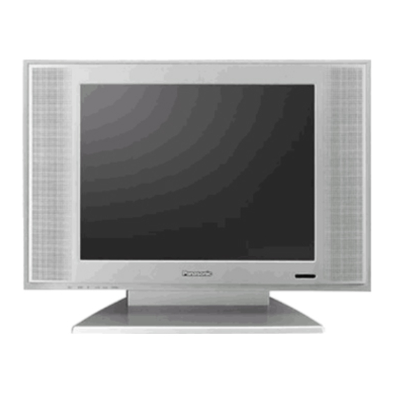
LCD Television
TX-20LB5F(WEST EUROPE)
TX-20LB5P(EAST EUROPE)
SL-115P Chassis
NTSC (AV input only)
Playback From NTSC video
recorders (VCR)
Aerial-ear
UHF / VHF
Operating Conditions
Temperature : 5-35°...
Humidity : 5%-90% RH (non-
condensing)
Connection Terminals
AV1 (Scart connecter)
21 Pin socket (Audio/Video in,
Audio/Video out, RGB in)
AV2
VIDEO
RCA PIN Type * 1
S-VIDEO
Mini DIN 4-pin
AUDIO L-R
RCA PIN Type * 2
Dimensions (W * H * D)
Including TV Stand
608mm * 215mm * 457.5mm
TV Set Only
608mm * 73.7mm * 403mm
Weight (Mass)
10.1Kg NET
Note :
Specifications are subject to
change without notice.
Weights and dimensions
shown are approximate.
2005 Matsushita Electric Industrial Co., Ltd.
All rights reserved. Unauthorized copying and
distribution is a violation of law.
Advertisement
Table of Contents

Subscribe to Our Youtube Channel
Related Manuals for Panasonic TX-20LB5F


Summary of Contents for Panasonic TX-20LB5F
- Page 1 ORDER No. PCZ0511109C2 LCD Television TX-20LB5F(WEST EUROPE) TX-20LB5P(EAST EUROPE) SL-115P Chassis SPECIFICATIONS Power Source NTSC (AV input only) “AC 100-240V, 50/60Hz” Playback From NTSC video Power Consumption recorders (VCR) Average use : 50W Aerial-ear Stand-by condition : 2.5W UHF / VHF “TV set DC 15V, 3.5A max”...
-
Page 2: Table Of Contents
Design and Specifications are subject to change without notice. Weight and Dimensions shown are approximate. WARNING This service information is designed for experienced repair technicians only and is not designed for use by the general public. It does not contain warnings or cautions to advise non-technical individuals of potential dangers in attempting to service a product. Products powered by electricity should be serviced or repaired only by experienced professional technicians. -
Page 3: Safety Precautions
1. Safety Instruction 1.1. General Guidelines 1. When servicing, observe the original lead dress. If a short circuit is found, replace all part which have been overheated or damaged by the short circuit. 2. After servicing, see to it that all the protective devices such as insulation barriers, insulation papers shields are properly installed. -
Page 4: Prevention Of Electro Static Discharge(Esd) To Electrostatically Sensitive(Es) Devices
2 Prevention of Electro Static Discharge (ESD) to Electrostatically Sensitive(ES) Devices Some semiconductor (solid state) devices can be damaged easily by static electricity. Such components commonly are called Electrostatically Sensitive (ES) Devices. Examples of typical ES devices are integrated circuits and some field-effect transistors and semiconductor “chip” components. -
Page 5: Chasis Board Layout
3. C has sis B oard Layout B oard Name F unction A-B oard MAIN P C B B -B oard INV E R T E R P C B C -B oard AV P C B D-B oard IR /LE D P C B E -B oard C ONT R OL P C B... -
Page 6: Servicing Method
4. Servicing method 4.1. Removing the tilt base 4.2. Removing the rear cover 1. Lay down the main unit so that the rear 1. Remove the tilt base.(See 4.1.) cover faces upward. 2. Remove the fixing screw(8pcs) 2. Remove the fixing screw(4pcs). 3. -
Page 7: Removing The Switch Unit
Servicing method 4.3. Removing the switch unit 4.5. Removing the C-Board 1. Remove the rear cover. (See 4.2.) 1. Remove the rear cover. (See 4.2.) 2. Disconnect the coupler. (E1) 2. Disconnect the coupler. (C1) 3. Remove the fixing screw. (1pcs) 3. -
Page 8: Removing The D-Board
Servicing method 4.7. Removing the D-Board 4.9. Removing the Shield pcb assy 1. Remove the IR/LED unit. (See 4.6.) 1. Remove the fixing screws. (8pcs) 2. Remove the fixing screws. (2pcs) 2. Disconnect the coupler. 3. Remove the D-Board. (C1), (D1), (E1), (S1) 3. -
Page 9: Removing The A-Board, B-Board
Servicing method 4.11. Removing the A-board, B-board 1. Remove the Shield pcb assy. (See 4.10.) 2. Disconnect the coupler. (A1), (A2), (B1), (B2), (B3) 3. Remove the fixing screws. (8pcs) 4. Remove the A-Board, B-Board. 4.12. Removing the LCD panel 1. -
Page 10: Service Mode Function
5. Service Mode Function 1. When entering the Service mode, it is necessary to enter the PR99 of the TV mode. (1) Service Mode 1 INPUT: Teletext R key --> Telextext G key --> Telextext Y key --> MENU key --> Ambience key Service Mode1 Main Menu... -
Page 11: Conductor Views
6. Conductor Views 6.1. MAIN PCB (TOP) PPART LOCATION TRANSISTOR IC10 IC11 IC12 IC13 IC14 IC15 IC16 IC17 IC18 IC19 IC20 IC21 IC22 IC23 IC24 IC25 IC26 IC27 IC29 IC30 IC31 IC33 IC34 IC35 IC38 IC39 IC40... -
Page 12: Main Pcb(Bottom)
Conductor Views 6.2. MAIN PCB (BOTTOM) -
Page 13: Block And Schematic Diagrams
7 Block and Schematic Diagrams 7.1. Schematic Diagram Notes Important Safety Notice Components identified by mark have special characteristics important for safety. When replacing any of these components, use only manufacture’s specified parts. Notes: Remarks: 1. Resistor 1. The Power Circuit contains a circuit area which uses a separate power supply to All resistors are cabon 1/4W resistor, unless marked as follows: isolate the earth connection. -
Page 14: Signal Block Diagram
Block and Schematic Diagrams 7.2. Signal Block Diagram Signal Block TXD RXD Crystal FLASH SDRAM Tuner IF IN (LOC:TU1) 24bit 24bit V PORT VCT1 CVBS[AV2] GCLK VCLK MDIN-150 S-VHS[AV2/S] (LOC:IC29) Deinterlace RGB/CVBS SCART[AV1] (LOC:IC22) Panel EXT Audio [AV2 Sound] D PORT VPEN Audio MUX VFIELD... -
Page 15: Power Schematic Diagram
Block and Schematic Diagrams 7.3. Power Schematic Diagram... -
Page 16: Vcti Schematic Diagram
Block and Schematic Diagrams 7.4. VCTI Schematic Diagram... -
Page 17: Memory Amp Schematic Diagram
Block and Schematic Diagrams 7.5. Memory AMP Schematic Diagram... -
Page 18: Ad9883 Schematic Diagram
Block and Schematic Diagrams 7.6. AD9883 Schematic Diagram... -
Page 19: Deinterlace Schematic Diagram
Block and Schematic Diagrams 7.7. Deinterlace Schematic Diagram... -
Page 20: Image Processor Schematic Diagram
Block and Schematic Diagrams 7.8. Image Processor Schematic Diagram... -
Page 21: Lvds, Key, Input Schematic Diagram
Block and Schematic Diagrams 7.9. LVDS, Key, Input Schematic Diagram... -
Page 22: Parts Location & Mechenical Replacement Parts List
8. Parts Location & Mechanical Replacement Parts List 8.1. Parts Location... -
Page 23: Packing Exploded View
Parts Location & Mechanical Replacement Parts List 8.2. Packing Exploded View... -
Page 24: Service Parts List
4858317110 SPEAKER SP-5090N04 C131 HCBK104KBA C CHIP CERA 50V X7R 0.1MF K 1608 ZZ290 PTMPMSG096F PCB MAIN MANUAL AS DLP-20D4LHS TX-20LB5F C134 HCBK104KBA C CHIP CERA 50V X7R 0.1MF K 1608 ZZ290 PTMPMSG096P PCB MAIN MANUAL AS DLP-20D4LHS TX-20LB5P C139... - Page 25 Service Part List PART CODE PART NAME DESCRIPTION REMARK PART CODE PART NAME DESCRIPTION REMARK C147 HCBK104KBA C CHIP CERA 50V X7R 0.1MF K 1608 C274 HCBK104KBA C CHIP CERA 50V X7R 0.1MF K 1608 C154 HCBK104KBA C CHIP CERA 50V X7R 0.1MF K 1608 C276 HCBK104KBA...
- Page 26 Service Part List PART CODE PART NAME DESCRIPTION REMARK PART CODE PART NAME DESCRIPTION REMARK DZ02W5R6VA DIODE CHIP ZENER Z02W5.6V R250 HRFT101JBA R CHIP 1/10 100 OHM J 1608 DZ02W5R6VA DIODE CHIP ZENER Z02W5.6V R254 HRFT000-BA R CHIP 1/10 0 OHM 1608 DBAV70—-B DIODE CHIP BAV70...
- Page 27 Service Part List PART CODE PART NAME DESCRIPTION REMARK PART CODE PART NAME DESCRIPTION REMARK C115 HCBK104KBA C CHIP CERA 50V X7R 0.1MF K 1608 C301 HCELF471ME C CHIP ELECTRO 16V 470MF CM 8010 C116 HCELF220MD C CHIP ELECTRO 16V 22MF CM 4052 C303 HCELH100MC C CHIP ELECTRO 25V 10MF CM 4052...
- Page 28 Service Part List PART CODE PART NAME DESCRIPTION REMARK PART CODE PART NAME DESCRIPTION REMARK IC15 1A1117E18D IC CHIP REGULATOR AP1117E18A 1.8V 2% SOT-223 HFRMZA600A F CHIP BEAD ARRARY 60 OHM MZA 3216Y IC16 19883C110Q IC CHIP ADC MST9883CR-110 MSPS HFRMZA600A F CHIP BEAD ARRARY 60 OHM MZA 3216Y...
- Page 29 Service Part List PART CODE PART NAME DESCRIPTION REMARK PART CODE PART NAME DESCRIPTION REMARK R161 HRFT472JBA R CHIP 1/10 4.7K OHM J 1608 HRFT151JBA R CHIP 1/10 150 OHM J 1608 R163 HRFT000-BA R CHIP 1/10 0 OHM 1608 HRFT330JBA R CHIP 1/10 33 OHM J 1608...
Need help?
Do you have a question about the TX-20LB5F and is the answer not in the manual?
Questions and answers