Philips HTS 3544 Service Manual
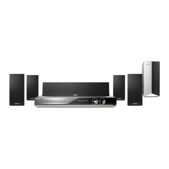
Dvd micro theatre
Hide thumbs
Also See for HTS 3544:
- User manual (57 pages) ,
- Quick start manual (2 pages) ,
- Specifications (3 pages)
Table of Contents
Advertisement
DV D Micro T heatre
S ervice
S ervice Manual
Copyright 2007 Philips Consumer Electronics B.V. Eindhoven, The Netherlands
©
All rights reserved. No part of this publication may be reproduced, stored in a retrieval system or
transmitted, in any form or by any means, electronic, mechanical, photocopying, or otherwise
without the prior permission of Philips.
Published by HY-ET0702 Service Audio Printed in The Netherlands Subject to modification
Version 1.0
TABLE OF CONTENTS
Location of PC Boards ................................................ 1-2
Versions Variation & Package .................................... 1-2
Specifications .............................................................. 1-3
Service Aids ................................................................ 1-4
ESD & Safety Instruction ............................................ 1-5
Lead-free solding Information .................................... 1-6
Repair Instructions ......................................................... 2
Disassembly Instructions & Service positions .............. 3
Block & Wiring Diagram ................................................ 4
Ipod Board ..................................................................... 5
Control Board ................................................................. 6
Main Board ..................................................................... 7
Power Board .................................................................. 8
DVD loader....................................................................9
Mechanical Exploded View & Parts..............................10
1 - 1
Page
HT S 3544/
37
HT S 3555/
37
3139 785 32480
Advertisement
Table of Contents

Related Manuals for Philips HTS 3544


Summary of Contents for Philips HTS 3544
- Page 1 Power Board ..............8 DVD loader..............9 Mechanical Exploded View & Parts......10 Copyright 2007 Philips Consumer Electronics B.V. Eindhoven, The Netherlands © All rights reserved. No part of this publication may be reproduced, stored in a retrieval system or transmitted, in any form or by any means, electronic, mechanical, photocopying, or otherwise without the prior permission of Philips.
-
Page 2: Location Of Pcb Boards
1 - 2 LOCATION OF PCB BOARDS IPOD PCB MAIN PCB STANDBY PCB POWER PCB CONTROL PCB MP3 PCB USB PCB VERSION VARIATION: HTS3544 Type/Versions Features & Board in used Main (Output Power-1000W) Composite Video Out Power Voltage (120V) AC Cord (Fix) -
Page 3: Speci Cations
1 - 3 Speci cations AMPLIFIER FRONT AND REAR SPEAKERS Total output power System ............Full range satellite - Home Theater mode ........... 1000 W Impedance ................6 - FTC* output power ............510 W Speaker drivers .........3” full range speaker Frequency Response ...... -
Page 4: Service Aids
1 - 4 SERVICE AIDS Service Tools: Universal Torx driver holder .........4822 395 91019 Torx bit T10 150mm ...........4822 395 50456 Torx driver set T6-T20 .........4822 395 50145 Torx driver T10 extended ........4822 395 50423 Compact Disc: SBC426/426A Test disc 5 + 5A ......4822 397 30096 SBC442 Audio Burn-in test disc 1kHz ....4822 397 30155 SBC429 Audio Signals disc .........4822 397 30184 Dolby Pro-logic Test Disc ........4822 395 10216... -
Page 5: Class 1 Laser Product
1 - 5 WAARSCHUWING WARNING Alle IC’s en vele andere halfgeleiders zijn All ICs and many other semi-conductors are gevoelig voor electrostatische ontladingen susceptible to electrostatic discharges (ESD). (ESD). Careless handling during repair can reduce life Onzorgvuldig behandelen tijdens reparatie kan drastically. - Page 6 Due to lead-free technology some rules have to be Philips-sets respected by the workshop during a repair: You will find this and more technical information Use only lead-free solder alloy Philips SAC305 with • within the “magazine”, chapter “workshop news”. order code 0622 149 00106. If lead-free solder-paste...
-
Page 7: Repair Instructions
2 - 1 2 - 1 REPAIR INSTRUCTION (Part One) MA IN UNIT REPAIR CHART 1/ 3 Po wer Su pply A ll F unctio n Ip od inpu t A udi o line IN CO AX IA L In A ll F unctio n Wi reless DVD A udi o... - Page 8 2 - 2 2 - 2 REPAIR INSTRUCTION (Part Two) MA IN UNIT REPAIR CHART 2/ 3 DVD Audi o Ipod inpu t IN T Check JK 302 AUX/TV IN Check IC 801 Change this JK No S ound No S ound A nd It s co nj oi nt part s IN T or No No Output...
- Page 9 2 - 3 2 - 3 REPAIR INSTRUCTION (Part Three) MA IN UNIT REPAIR CHART 3/3 Tuner No Sound Check SW Power Output See B HDMI No Output No Svideo output No Y Pr Pb output FM Function No Sound Check CN302 IC301 Check CN301 Q901ZD904 Check CN301 Pin9= +9V...
-
Page 10: Ipod Board
3 - 1 3 - 1 DISASSEMBLY INSTRUCTIONS 2) Return the set to its upright position and remove the Tray Dismantling of the Main PCB Cover as shown in Figure 3 and close the tray manually by 2) Loosen 3 screw “ A “ on the top of main board as shown in pushing it back in. -
Page 11: Service Positions
3 - 2 3 - 2 Dismantling of the Control Board SERVICE POSITIONS 1) Loosen 10 screws “E” at the back pancle as shown in gure 6 Service position A Figure 6 Dismantling of the Power Board Dismantling of the DVD Module 1) Loosen 5 screws “D”... -
Page 12: Block Diagram
4 - 1 4 - 1 BLOCK DIAGRAM PHONE JACK SP DIF IN IC MP3-IN TV-I N AUX-IN SIRIUS SA TELLI TE RADIO USB SOCKET CS8415 COAXIAL INPUT IC TC4051BPx 2 SWITCH S-VIDEO AMPLIFIER AMPLIFIER Panasonic TUNER MT1389HD u_co m C-VIDEO SYSTEM IC IRC4558... -
Page 13: Wiring Diagram
4 - 2 4 - 2 WIRING DIAGRAM... - Page 14 5 - 1 IPOD BOARD TABLE OF CONTENTS Circuit Diagram .................. 5-2 PCB Layout Top & Bottom View ............5-3...
-
Page 15: Circuit Diagram
5 - 2 CIRCUIT DIAGRAM C117 CN100 A2 R175 R210 C118 F101 R176 R211 F101 FUSE SIRIUS5V 700MA CN100 R210 Sir_L C118 R211 Sir_R C117 DIJK JK101 TO HTS3540 TO Ipod CJD008202-1010... -
Page 16: Pcb Layout Top View
5 - 3 PCB LAYOUT TOP VIEW CN100 A1 JK101 PCB LAYOUT Bottom VIEW C117 B1 F101 A1 R176 B1 R211 B1 C118 B1 R175 B1 R210 B1... -
Page 17: Ftd Display Pin Assignment
6 - 1 6 - 1 FTD DISPLAY PIN ASSIGNMENT CONTROL BOARD TABLE OF CONTENTS FTD Display Pin Assignment ............. 6-1 Voltage ....................6-2 Circuit Diagram .................. 6-3 PCB Layout Top & Bottom View ............6-4 Note... - Page 18 6 - 2 6 - 2 VOLTAGE IC251 Pin NO Voltage 4.70 -23.00 -26.00 -23.00 -23.00 -21.00 -21.00 -23.00 -23.00 -21.00 -21.00 -23.00 -23.00 -23.00 -26.00 -21.00 -26.00 -26.00 -23.00 4.70 Pin NO Voltage -26.00 -23.00 -23.00 -22.00 -22.00 -24.00 -24.00 -24.00 -24.00 -24.00 -24.00 4.70 4.70 0.00...
- Page 19 6 - 3 6 - 3 CIRCUIT DIAGRAM C2501 A3 C2509 A2 C2515 B1 C2522 B1 C2528 A1 C2540 B2 D2507 B1 FB35 JMP11 B3 JMP5 LD2501 B3 R2503 A1 R2509 A1 R2517 B1 R2523 B1 R2530 A1 R2540 A1 R2549 A1 RB903 A1 TA2507 B1...
- Page 20 6 - 4 6 - 4 PCB LAYOUT - TOP VIEW C2504 C2531 D2504 JMP1 JMP14 JMP3 JMP7 R2502 R2528 R2540 RB5501 A3 SN251 TA2506 B1 TA2511 B1 XL2501 B2 C2505 D2501 D2507 JMP11 JMP15 JMP5 JMP8 R2508 R2532 RB201 RB903 TA2501 A3 TA2507 B1...
-
Page 21: Main Board
7 - 1 7 - 1 INTERNAL IC DIAGRAM - CO4558A HOSP MAIN BOARD TABLE OF CONTENTS Internal IC Diagram ................7-1 Circuit Diagram (Ampli er - Top Left) ..........7-2 Circuit Diagram (Ampli er - Top Right) ..........7-3 Circuit Diagram (Ampli er - Bottom Left) ........... - Page 22 7 - 2 7 - 2 Circuit Diagram (Ampli er - Top Left) C0101 C530 C922 C0102 C531 C923 C0103 C532 C924 C0104 C533 C925 C0105 C534 C926 C0106 C535 C927 C0107 C536 C928 C0109 C537 C929 C0110 C538 C930 C0111 C539 C931...
- Page 23 7 - 3 7 - 3 Circuit Diagram (Ampli er - Top Right) D704 R316 R908 D705 R317 R909 D706 R318 R911 D707 R319 R912 D708 R320 R913 D709 R321 R914 D710 R322 R918 D711 R323 R919 D712 R324 R920 D901 R325 R921...
- Page 24 7 - 4 7 - 4 Circuit Diagram (Ampli er - Bottom Left)
- Page 25 7 - 5 7 - 5 Circuit Diagram (Ampli er - Bottom Right)
- Page 26 7 - 6 7 - 6 Circuit Diagram (Servo - Top Left) C0201 C253 C0202 C254 C0203 C300 C0204 C601 C0205 C602 C0206 C604 C0207 C605 C0208 C606 C0209 C607 C0210 C608 C0212 C609 C0213 C610 C0214 C611 C0215 C612 C0216 C801 C0217...
- Page 27 7 - 7 7 - 7 Circuit Diagram (Servo - Top Right) D205 R253 R255 FB201 A3 R256 FB202 A3 R257 FB203 A3 R258 FB204 A3 R260 FB205 C5 R261 FB206 C5 R263 FB207 D5 R266 FB208 D5 R269 FB209 C1 R271 FB210 C1 R272...
- Page 28 7 - 8 7 - 8 Circuit Diagram (Servo - Bottom Left)
- Page 29 7 - 9 7 - 9 Circuit Diagram (Servo - Bottom Right)
- Page 30 7 - 10 7 - 10 PCB Layout Top View C0114 D2 C204 C302 C352 C520 C576 C707 C812 C844 C932 D205 FB202 A4 FB602 A5 IC208 L203 L703 Q905 R221 R255 R303 R331 R377 R517 R611 R819 R909 R944 C0115 A3 C205 C303...
- Page 31 7 - 11 7 - 11 PCB Layout Bottom View C0101 C0112 C0209 C0226 C0242 C0502 C0609 C232 C320 C5003 C535 C553 C563 C587 C730 C835 C939 CE206 CE506 CE804 D906 Q705 R399 R528 R621 R952 C0102 C0113 C0210 C0228 C0243 C0504 C0612...
- Page 32 7 - 12 7 - 12 VOLTAGE IC201 IC301 Pin NO Pin NO Voltage 0.00 0.00 0.00 -13.00 0.00 0.00 0.00 12.00 Voltage 3.30 0.00 0.00 2.50 2.50 5.10 0.00 0.00 3.30 2.50 5.10 1.80 0.00 0.00 0.00 5.00 5.00 0.00 5.00 0.00 Pin NO...
-
Page 33: Power Board
8 - 1 8 - 1 VOLTAGE IC901 Pin NO Voltage 4.80 4.80 2.40 0.00 1.70 3.40 0.00 12.00 2.30 2.30 12.00 12.00 4.90 4.90 2.40 0.00 IC902 Pin NO Voltage 2.70 0.00 0.50 2.10 0.00 1.00 11.00 4.90 IC903 Pin NO Voltage 4.90... - Page 34 8 - 2 8 - 2 CIRCUIT DIAGRAM BD901 A1 C913 C924 C934 C945 C956 C966 C978 D909 D920 IC902 L903 Q907 Q917 R911 R923 R933 R944 R958 R968 R978 R988 TVR902 A1 ZD910 D5 C901 C914 C925 C935 C946 C957 C967 CN903 A5...
- Page 35 8 - 3 8 - 3 PCB LAYOUT - TOP VIEW BD901 C915 C934 C945 C954 C962 C970 CN904 D917 D923 IC901 J903 J913 J921 J927 J933 L904 Q904 Q911 R903 R915 R939 R949 R966 R990 TVR903 C1 C901 C916 C937 C949 C955...
- Page 36 8 - 4 8 - 4 PCB LAYOUT - BOTTOM VIEW C904 B3 C911 A2 C925 C2 C930 C2 C941 C3 C959 B2 D901 B3 D910 B3 Q906 C1 R911 B1 R920 B1 R925 C1 R929 A4 R947 B1 R955 C1 R963 C2 R972 C2 R977 B1...
-
Page 37: Dvd Board
9 - 1 DVD BOARD TABLE OF CONTENTS EXPLORER VIEW ................9-2... - Page 38 9 - 2 EXPLORER VIEW...
- Page 39 10 - 1 10 - 1 Mechanical Exploded View...
Need help?
Do you have a question about the HTS 3544 and is the answer not in the manual?
Questions and answers