Table of Contents
Advertisement
Quick Links
See also:
User Manual
DVD Hometheater System
Service
Service Manual
©
Copyright 2007 Philips Consumer Electronics B.V. Eindhoven, The Netherlands
All rights reserved. No part of this publication may be reproduced, stored in a retrieval system or
transmitted, in any form or by any means, electronic, mechanical, photocopying, or otherwise
without the prior permission of Philips.
Published by KC-ET0412 Service Audio Printed in The Netherlands Subject to modification
Version 1.0
TABLE OF CONTENTS
Location of PC Boards ................................................ 1-2
Versions Variation & Package .................................... 1-2
Specifications .............................................................. 1-3
Service Aids ................................................................ 1-4
ESD & Safety Instruction ............................................ 1-5
Lead-free solding Information .................................... 1-6
Repair Instructions ......................................................... 2
Disassembly Instructions & Service positions .............. 3
Block & Wiring Diagram ................................................ 4
Control Board ................................................................. 5
Main Board ..................................................................... 6
Power Board .................................................................. 7
DVD loader....................................................................8
Mechanical Exploded View & Parts...............................9
1 - 1
Page
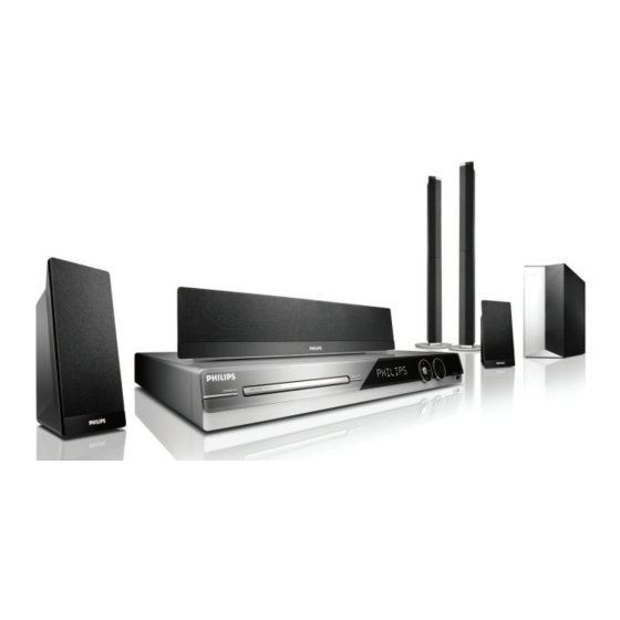
HTS3548/
98/51
Advertisement
Table of Contents

Related Manuals for Philips HTS3548/51


Summary of Contents for Philips HTS3548/51
- Page 1 Mechanical Exploded View & Parts.......9 © Copyright 2007 Philips Consumer Electronics B.V. Eindhoven, The Netherlands All rights reserved. No part of this publication may be reproduced, stored in a retrieval system or transmitted, in any form or by any means, electronic, mechanical, photocopying, or otherwise without the prior permission of Philips.
-
Page 2: Location Of Pcb Boards
1 - 2 LOCATION OF PCB BOARDS MAIN PCB STANDBY PCB POWER PCB CONTROL PCB MIC VOL PCB PHONE JACK PCB USB PCB VERSION VARIATION: Type/Versions HTS3548 Features & Board in used Main (Output Power-1000W) Composite Video Out Power Voltage (120/230V) AC Cord (Detachable) - Page 3 1 - 3 Speci cations (red colour for/51) AMPLIFIER MAIN UNIT Total output power: ............1000W Power Supply Rating: ......110-127 V / 220-240 V~ Frequency Response: ....... 180 Hz – 14 kHz / ±3 dB ..............50-60 Hz switchable Signal-to-Noise Ratio: ......>...
-
Page 4: Service Aids
1 - 4 SERVICE AIDS Service Tools: Universal Torx driver holder .........4822 395 91019 Torx bit T10 150mm ...........4822 395 50456 Torx driver set T6-T20 .........4822 395 50145 Torx driver T10 extended ........4822 395 50423 Compact Disc: SBC426/426A Test disc 5 + 5A ......4822 397 30096 SBC442 Audio Burn-in test disc 1kHz ....4822 397 30155 SBC429 Audio Signals disc .........4822 397 30184 Dolby Pro-logic Test Disc ........4822 395 10216... - Page 5 1 - 5 WAARSCHUWING WARNING Alle IC’s en vele andere halfgeleiders zijn All ICs and many other semi-conductors are gevoelig voor electrostatische ontladingen susceptible to electrostatic discharges (ESD). (ESD). Careless handling during repair can reduce life Onzorgvuldig behandelen tijdens reparatie kan drastically.
- Page 6 Due to lead-free technology some rules have to be Philips-sets respected by the workshop during a repair: You will find this and more technical information Use only lead-free solder alloy Philips SAC305 with • within the “magazine”, chapter “workshop news”. order code 0622 149 00106. If lead-free solder-paste...
-
Page 7: Ma In Unit Repair Chart
2 - 1 2 - 1 REPAIR INSTRUCTION (Part One) MA IN UNIT REPAIR CHART 1/ 3 Po wer Su pply A ll F unctio n A udi o line IN CO AX IA L In A ll F unctio n DVD A udi o MP 3 In T uner No So und... - Page 8 2 - 2 2 - 2 REPAIR INSTRUCTION (Part Two) MA IN UNIT REPAIR CHART 2/3 DVD Audio AUX/TV IN COAXIAL In Check IC801 Check JK302 No Output No Sound And Its conjoint parts No Sound Change this JK INT or No Check CN802 CN803 Check JK302 Check JK702 Pin5...
- Page 9 2 - 3 2 - 3 REPAIR INSTRUCTION (Part Three) MA IN UNIT REPAIR CHART 3/3 Tuner No Sound Check SW Power Output See B HDMI No Output No Svideo output No Y Pr Pb output FM Function No Sound Check CN302 IC301 Check CN301 Q901ZD904 Check CN301 Pin9= +9V...
- Page 10 3 - 1 3 - 1 DISASSEMBLY INSTRUCTIONS 2) Return the set to its upright position and remove the Tray Dismantling of the Main PCB Cover as shown in Figure 3 and close the tray manually by 2) Loosen 3 screw “ A “ on the top of main board as shown in pushing it back in.
-
Page 11: Service Positions
3 - 2 3 - 2 Dismantling of the Control Board SERVICE POSITIONS 1) Loosen 12 screws “E” at the back pancle as shown in gure 6 Service position A Figure 6 Dismantling of the Power Board Dismantling of the DVD Module 1) Loosen 5 screws “D”... -
Page 12: Block Diagram
4 - 1 4 - 1 BLOCK DIAGRAM PHONE JACK SP DIF IN IC MP3-IN TV-I N AUX-IN USB SOCKET CS8415 COAXIAL INPUT IC TC4051BPx 2 SWITCH S-VIDEO AMPLIFIER AMPLIFIER Panasonic TUNER MT1389HD u_co m C-VIDEO SYSTEM IC IRC4558 A/D IC CS5340 IC IRC4558 MT1392E IP4776C Z38... -
Page 13: Wiring Diagram
4 - 2 4 - 2 WIRING DIAGRAM... -
Page 14: Ftd Display Pin Assignment
5 - 1 5 - 1 FTD DISPLAY PIN ASSIGNMENT CONTROL BOARD TABLE OF CONTENTS FTD Display Pin Assignment ............. 5-1 Voltage ....................5-2 Circuit Diagram .................. 5-3 PCB Layout Top & Bottom View ............5-4 Note... - Page 15 5 - 2 5 - 2 VOLTAGE IC251 Pin NO Voltage 4.70 -23.00 -26.00 -23.00 -23.00 -21.00 -21.00 -23.00 -23.00 -21.00 -21.00 -23.00 -23.00 -23.00 -26.00 -21.00 -26.00 -26.00 -23.00 4.70 Pin NO Voltage -26.00 -23.00 -23.00 -22.00 -22.00 -24.00 -24.00 -24.00 -24.00 -24.00 -24.00 4.70 4.70 0.00...
-
Page 16: Circuit Diagram
5 - 3 5 - 3 CIRCUIT DIAGRAM C2501 C2510 C2518 C2525 C2538 D2503 FB32 JMP2 R2503 R2510 R2519 R2526 R2535 R2542 R2555 TA2501 VR2502 A3 C2502 C2511 C2519 C2526 C2539 D2504 FB33 JMP3 LD2501 B3 R2504 R2513 R2520 R2528 R2536 R2544 RB201... -
Page 17: Pcb Layout - Top View
5 - 4 5 - 4 PCB LAYOUT - TOP VIEW C2504 A2 C2531 B2 D2503 B2 D2508 A2 JMP11 A3 JMP15 A2 JMP5 JMP8 R2508 B2 R2532 B3 R2538 B3 RB201 B2 RB903 B2 TA2501 A3 TA2507 B1 TA2516 A3 C2505 B2 CN5502 A1 D2504 B2... -
Page 18: Main Board
6 - 1 6 - 1 INTERNAL IC DIAGRAM - CO4558A HOSP MAIN BOARD TABLE OF CONTENTS Internal IC Diagram ................6-1 Circuit Diagram (Ampli er) ..............6-2 Circuit Diagram (Servo) ..............6-3 PCB Layout Top View ............... 6-4 PCB Layout Bottom View ..............6-5 Voltage .................... - Page 19 6 - 2 6 - 2 Circuit Diagram (Ampli er) C0101 D4 C5008 C5 C587 CE504 C5 JP505A A5 R345 R571 C0102 D4 C501 C588 CE505 C5 JP507 R346 R572 C0103 D4 C502 C589 CE506 C5 JP507A A5 R347 R573 C0104 D4 C503 C590...
- Page 20 6 - 3 6 - 3 Circuit Diagram (Servo) C0201 C2 C229 CE802 D2 R210 R801 C0202 A3 C230 CE803 D2 R211 R802 C0203 A3 C231 CE804 D2 R212 R803 C0204 A3 C232 CE805 D2 R216 R804 C0205 A3 C233 CE806 D2 R217 R805...
- Page 21 6 - 4 6 - 4 PCB Layout Top View C0114 D2 C209 B4 C334 A4 C503 A2 C541 A2 C610 B5 C810 D5 C849 C5 C947 B5 D705 B4 FB302 C5 FB906 B3 JP507 B1 L703 Q907 A2 R228 D4 R272 C3 R326 A3 R356 A3...
- Page 22 6 - 5 6 - 5 PCB Layout Bottom View C0101 A4 C0117 D4 C0217 B4 C0238 B4 C0252 B4 C0609 A5 C238 C5 C322 C5007 A2 C549 C561 D2 C587 C3 C802 D5 C903 D3 C954 CE502 A1 CE802 D4 D906 R220 R523...
- Page 23 6 - 6 6 - 6 VOLTAGE IC201 IC301 Pin NO Pin NO Voltage 0.00 0.00 0.00 -13.00 0.00 0.00 0.00 12.00 Voltage 3.30 0.00 0.00 2.50 2.50 5.10 0.00 0.00 3.30 2.50 5.10 1.80 0.00 0.00 0.00 5.00 5.00 0.00 5.00 0.00 Pin NO...
-
Page 24: Power Board
7 - 1 7 - 1 VOLTAGE IC901 Pin NO Voltage 4.80 4.80 2.40 0.00 1.70 3.40 0.00 12.00 2.30 2.30 12.00 12.00 4.90 4.90 2.40 0.00 IC902 Pin NO Voltage 2.70 0.00 0.50 2.10 0.00 1.00 11.00 4.90 IC903 Pin NO Voltage 4.90... - Page 25 7 - 2 7 - 2 CIRCUIT DIAGRAM BD901 A1 C914 C926 C938 C950 C961 C972 D904 D917 GT902 C1 L903 Q908 R902 R916 R926B D2 R939 R952 R964 R975 R986 TVR901 A1 ZD910 D5 C901 C915 C927 C939 C951 C962 C973 D905...
- Page 26 7 - 3 7 - 3 PCB LAYOUT - TOP VIEW BD901 A1 C920 C943 C954 C964 C977 D913 D924 IC905 C3 J912 J922 J930 L903 Q905 Q914 R909 R940 R961 R987 ZD901 B2 C901 C921 C944 C955 C965 CN901 A1 D917 D925 J901...
- Page 27 7 - 4 7 - 4 PCB LAYOUT - BOTTOM VIEW C904 C911 C925 C930 C941 C959 D901 D910 Q906 C1 R911 R920 R925 R927 R933 R952 R960 R970 R975 R981 R989 ZD903 B1 ZD912 B1 C906 C917 C926 C931 C942 C968 D905...
-
Page 28: Dvd Board
8 - 1 DVD BOARD TABLE OF CONTENTS EXPLORER VIEW ................8-2 MECHANICAL PART LIST ..............8-3... - Page 29 8 - 2 EXPLORER VIEW...
-
Page 30: Mechanical Part List
8 - 3 MECHANICAL PART LIST Loc. Part No. Description BPM206009-0202 TRAY FMT020202-XXXX TRAY MOTOR HSP243174-1030 SCREW BPG206006-0001 GEAR-G POM BPG206014-0001 GEAR PULLER POM HSW258064-1040 SCREW BPG206026-0001 GEAR TRAY1 BPG206027-0001 GEAR TRAY - 2 BPG206028-0001 GEAR TRAY - 3 HSW248004-1060 SCREW BRW206004-0001 RUBB BELT... - Page 31 9 - 1 9 - 1 Mechanical Exploded View...
-
Page 32: Dvd Loader
HTS3548/51 0001 996510003872 DISPLAY LENS 0010 996510001262 FUNCTION BUTTON 0011 996510005043 DVD DOOR 0012 996510003835 SOURCE BUTTON 0013 996510003836 SOURCE BUTTON HOLDER 0014 996510005041 BRACKET PCB 0015 996510003837 VFD FILTER 0002 996510003873 FRONT CABINET 0025 996510001615 FAN COVER 0027 994000005305 RUBBER FOOT D14XT3.0MM W/ADV... - Page 33 HTS3548/98 0001 996510003872 DISPLAY LENS 0002 996510003873 FRONT CABINET 0003 996510001256 STANDY BUTTON 0004 996510001257 OPEN/CLOSE BUTTON 0005 996510001662 STANDY LED LENS 0006 996510003834 OPEN /CLOSE BUTTON HOLDER 0007 996510001663 FUNCTION BUTTON RING 0008 996510001664 VOLUME KNOB RING 0009 996510001261 VOLUME KNOB RING 0010 996510001262...
Need help?
Do you have a question about the HTS3548/51 and is the answer not in the manual?
Questions and answers