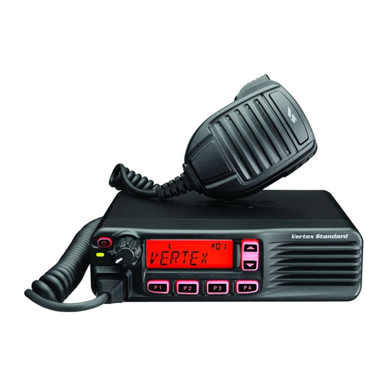
Vertex Standard VX-4600 Series Service Manual
Hide thumbs
Also See for VX-4600 Series:
- User manual (2 pages) ,
- Operating manual (33 pages) ,
- Product manual (28 pages)
Table of Contents
Advertisement
VHF FM Transceiver
VX-4500 Series
VX-4600 Series
Service Manual
©
2011VERTEX STANDARD CO., LTD.
VX-4500 Series
Introduction
This manual provides the technical information necessary for servicing the VX-4500/-4600 Series Mobile Transceiver.
Servicing this equipment requires expertise in handing surface-mount chip components. Attempts by non-qualified
persons to service this equipment may result in permanent damage not covered by the warranty, and may be illegal
in some countries.
Two PCB layout diagrams are provided for each double-sided board in this transceiver. Each side of the board is
referred to by the type of the majority of components installed on that side ("Side A" or "Side B"). In most cases one
side has only chip components (surface-mount devices), and the other has either a mixture of both chip and leaded
components (trimmers, coils, electrolytic capacitors, ICs, etc.), or leaded components only.
As described in the pages to follow, the advanced microprocessor design of the VX-4500/-4600 allows a complete
Alignment of this transceiver to be performed without opening the case of the radio; all adjustments can be performed
from the personal computer, using with the Vertex Standard FIF-10A USB Programming Interface and CE115 Soft-
ware.
While we believe the information in this manual to be correct, Vertex Standard assumes no liability for damage that
may occur as a result of typographical or other errors that may be present. Your cooperation in pointing out any
inconsistencies in the technical information would be appreciated.
The VX-4500/-4600 was assembled using Pb (lead) free solder, based on the RoHS specification.
Only lead-free solder (Alloy Composition: Sn-3.0Ag-0.5Cu) should be used for repairs performed on this apparatus. The
solder stated above utilizes the alloy composition required for compliance with the lead-free specification, and any solder
with the above alloy composition may be used.
Specifications ............................................................... 2
Dsub 15-Pin Accessory Connector .......................... 3
Exploded View & Miscellaneous Parts ................... 4
Block Diagram .............................................................. 5
Circuit Description ...................................................... 6
Alignment ..................................................................... 8
Installation Of Option ............................................... 22
EC093N90B
Important Note
Contents
Board Units (Schematics, Layouts & Parts)
Main Unit ............................................................. 23
Front-A Unit ( Vx-4500 ) .................................... 30
Front-B Unit ( Vx-4600 ) .................................... 37
Optional Units (Schematics, Layouts & Parts)
DVS-8 Voice Storage Unit .................................... 44
VERTEX STANDARD CO., LTD.
4-8-8 Nakameguro, Meguro-Ku, Tokyo 153-8644, Japan
VERTEX STANDARD
US Headquarters
10900 Walker Street, Cypress, CA 90630, U.S.A.
YAESU UK LTD.
Unit 12, Sun Valley Business Park, Winnall Close
Winchester, Hampshire, SO23 0LB, U.K.
VERTEX STANDARD HK LTD.
Unit 1306-1308, 13F., Millennium City 2, 378 Kwun Tong Road,
Kwun Tong, Kowloon, Hong Kong
VERTEX STANDARD ( AUSTRALIA ) PTY., LTD.
Tally Ho Business Park, 10 Wesley Court, East Burwood, VIC, 3151
VX-4600 Series
Advertisement
Table of Contents

Subscribe to Our Youtube Channel
Related Manuals for Vertex Standard VX-4600 Series


Summary of Contents for Vertex Standard VX-4600 Series
- Page 1 While we believe the information in this manual to be correct, Vertex Standard assumes no liability for damage that may occur as a result of typographical or other errors that may be present. Your cooperation in pointing out any inconsistencies in the technical information would be appreciated.
-
Page 2: Specifications
Specifications General Frequency Ranges: 134 -174 MHz Number of Channels: 8 channels (VX-4500 Series) 512 channels with 32 groups (VX-4600 Series) Power Supply Voltage: 13.6 V ± 20 % Channel Spacing: 12.5/20/25 kHz Pll Steps: 1.25/2.5/5/6.25 kHz Current Consumption (@13.6 V): 11 A (TX: 50 W), 6 A (TX: 25 W) 2.5 A (RX) -
Page 3: Dsub 15-Pin Accessory Connector
DSUB 15-pin Accessory Connector Pin 1: AF IN ( A Pin 6: EXT PTT NALOG NPUT External Microphone Input. Nominal input level is Shorting this port to ground causes the transceiver to 4 mV (or -10 dBm; programmed via the CE115 pro- be placed in the Transmit mode, while opening the grammer) at 600-ohm. -
Page 4: Exploded View & Miscellaneous Parts
Exploded View & Miscellaneous Parts Non-designated parts are available only as part of a designated assembly. VX-4500/-4600 Series VHF FM Transceiver Service Manual... -
Page 5: Block Diagram
Block Diagram VX-4500/-4600 Series VHF FM Transceiver Service Manual... -
Page 6: Circuit Description
Circuit Description 1. Circuit Configuration by Frequency 2-4. Audio amplifier Detected signal from Q1054 (NJM2591V) is delivered to The receiver is a double-conversion superheterodyne with a first Q1010 (FQ0801) and is output by Q1010 (FQ0801) pin 17 intermediate frequency (IF) of 50.85 MHz and a second IF of through the band pass filter. - Page 7 Circuit Description 3. Transmitter System 3-4-1. VCO While the radio is receiving, the RX oscillator Q1034 (2SK508) 3-1. Mic Amplifier in VCO generates a programmed frequency between 184.85 The AF signal from microphone jack J2001 (VX-4500) or J3001 and 224.85 MHz as 1st local signal. While the radio is transmit- (VX-4600) is amplified with microphone amplifier in Q1010 ting, the TX oscillator Q1036 (2SC3356) in VCO generates a (FQ0801), is amplified a second time after microphone selec-...
-
Page 8: Alignment
Frequency Counter: ±0.2 ppm accuracy at 200 MHz ponent replacement and service should be performed only AF Signal Generator by an authorized Vertex Standard representative, or the AC Voltmeter warranty policy may be voided. DC Voltmeter The following procedures cover the sometimes critical and ... - Page 9 Alignment Test Setup Setup the test equipment as shown for transceiver align- ment, apply 13.6V DC power to the transceiver. Refer to the drawings below for Alignment Points. The Alignment Tool Outline Installation of the alignment tool Install the CE115 (PC Programming Software) to your ...
- Page 10 Alignment Note: when all items are to be aligned, it is strongly rec- ommended to align them according to the following se- Alignment Mode quence. Detailed information for each step may be found The Alignment mode allows you to align the entire radio. in the “Help”...
- Page 11 Alignment 1. VCO (RX VCO/TX VCO) - Normally there is no need to adjust this parameter - This parameter is to align the VCO Voltage adjustment. 2. PLL Reference Frequency ( Frequency ) This parameter is to align the reference frequency for PLL. 1.
- Page 12 Alignment 3. RX Sensitivity (RX Tune) This parameter is to align the RX BPF (Band Pass Filter) for Receive (RX) sensitivity. The PLL Reference Frequency (Frequency) alignment must be done before this alignment is performed. 1. Press the “RX Tune” button to start the alignment. The RX Sensitivity Alignment window will appear.
- Page 13 Alignment 4. Squelch (SQL) This parameter is to align the SQL (Squelch) Sensitivity. There are several alignments as follows in the Squelch Sensitivity. Tight SQL Level (TI NSQ W/N) The Alignment for the Noise SQL Tight level at Wide (5k/ 4k) or Narrow (2.5k).
- Page 14 Alignment 5. TX Power This parameter is to align the “Power High”, “Power Low3”, “Power Low2” or “Power Low1” for the selected channel. 1. Press the “TX Pwr(H / L3 / L2 / L1)” button to start the alignment. The TX Power Alignment window will appear.
- Page 15 Alignment 6. Maximum Deviation <Wide> / <Narrow> This parameter is to align the “Maximum Deviation” (Wide/Narrow). It requires the appropriate JIG (Tuning Interface BOX). Connect the JIG and Test Equipment to the radio before the alignment is started. 1. Press the “Max Dev (W /N)” button to start the align- ment.
- Page 16 Alignment Please adjust the following items when needed. Modulation Balance <Wide> / <Narrow> (This Alignment is difficult.) This parameter is to align the “Modulation Balance” (Wide/Narrow). It needs the appropriate JIG (Tuning Interface BOX). Connect the JIG and Test Equipment to the radio before the align- ment is started.
- Page 17 Alignment CTCSS Deviation <Wide> / <Narrow> This parameter is to align CTCSS Deviation of the selected channel. 1. Press the “CTC Dev (W / N)” button to start the align- ment. The CTCSS Deviation Alignment window will appear. 2. Click the left mouse button on the slide bar or press the Up / Down arrow key, to select the desired chan- nel.
- Page 18 Alignment DCS Deviation <Wide> / <Narrow> This parameter is to align “DCS Deviation” of the selected channel. 1. Press the “DCS Dev (W / N)” button to start the align- ment. The DCS Deviation Alignment window will appear. 2. Click the left mouse button on the slide bar or press the Up / Down arrow key, to select the desired chan- nel.
- Page 19 Alignment DTMF Deviation This parameter is to align “DTMF Deviation”. 1. Press the “DTMF” button to start the alignment. The DTMF Alignment window will appear. 2. Click the “PTT” button or press the “SPACE” bar the radio starts to transmit on the Center frequency chan- nel.
- Page 20 Alignment VOX On Level This parameter is to align the “VOX On Level”. Set the Sensitivity of the VOX circuitry's input audio detector. 1. Press the “VOX ON Level” button to start the align- ment. The VOX ON Level window will appear. 2.
- Page 21 Alignment EXT AF OUT Level This parameter is to align the “EXT AF OUT Level”. Set the Low-level receiver output of pin 2 of the D-SUB Connector. 1. Press the “Ext AF Out” button to start the alignment. The Ext AF Out Level window will appear. 2.
-
Page 22: Installation Of Option
Case Cover. Installation is now complete. multi-chanel digital-access radio trunking system. Do not install all Optional Unit at onece Each optional Unit is easily programmed the configula- tions using a Vertex Standard CE115 programmer with an IBM PC-compatible computer. Figure 2 Figure 1... - Page 23 MAIN Unit (Lot. 1~3) Circuit Diagram VX-4500/-4600 Series VHF FM Transceiver Service Manual...
- Page 24 MAIN Unit (Lot. 1~3) Parts Layout (Side A) VX-4500/-4600 Series VHF FM Transceiver Service Manual...
- Page 25 MAIN Unit (Lot. 1~3) Parts Layout (Side B) VX-4500/-4600 Series VHF FM Transceiver Service Manual...
- Page 26 MAIN Unit (Lot. 4~) Circuit Diagram VX-4500/-4600 Series VHF FM Transceiver Service Manual...
- Page 27 MAIN Unit (Lot. 4~) Parts Layout (Side A) VX-4500/-4600 Series VHF FM Transceiver Service Manual...
- Page 28 MAIN Unit (Lot. 4~) Parts Layout (Side B) VX-4500/-4600 Series VHF FM Transceiver Service Manual...
-
Page 29: Main Unit
MAIN Unit Parts List DESCRIPTION VALUE TOL. MFR'S DESIG VXSTD P/N VERS. LOT SIDE LAY ADR PCB with Components CS2092701 CH:8, POW:50 CS2092702 CH:512, POW:50 CS2092703 CH:8, POW:25 CS2092704 CH:512, POW:25 Printed Circuit Board FR021500D FR021500G TOP COVER RA123420B PACKING PAD (COVER) RA1234300 SEMS SCREW... -
Page 30: Front-A Unit ( Vx-4500 )
FRONT-A Unit (VX-4500: Lot. 1~2) Circuit Diagram VX-4500/-4600 Series VHF FM Transceiver Service Manual... - Page 31 FRONT-A Unit (VX-4500: Lot. 1~2) Parts Layout (Side A) Parts Layout (Side B) VX-4500/-4600 Series VHF FM Transceiver Service Manual...
- Page 32 FRONT-A Unit (VX-4500: Lot. 3) Circuit Diagram VX-4500/-4600 Series VHF FM Transceiver Service Manual...
- Page 33 FRONT-A Unit (VX-4500: Lot. 3) Parts Layout (Side A) Parts Layout (Side B) VX-4500/-4600 Series VHF FM Transceiver Service Manual...
- Page 34 FRONT-A Unit (VX-4500: Lot. 4~) Circuit Diagram VX-4500/-4600 Series VHF FM Transceiver Service Manual...
- Page 35 FRONT-A Unit (VX-4500: Lot. 4~) Parts Layout (Side A) Parts Layout (Side B) VX-4500/-4600 Series VHF FM Transceiver Service Manual...
- Page 36 FRONT-A Unit Parts List DESCRIPTION VALUE TOL. MFR'S DESIG VXSTD P/N VERS. LOT SIDE LAY ADR PCB with Components CB5426001 CH:8 Printed Circuit Board FR021710B FR021710C FR021710D FRONT PANEL ASSY (8CH) RA124940A PACKING PAD (PANEL) RA1234400 RUBBER KNOB RA124700A VOLUME KNOB RA1245900 SPEAKER 5015134H02...
-
Page 37: Front-B Unit ( Vx-4600 )
FRONT-B Unit (VX-4600: Lot. 1~2) Circuit Diagram VX-4500/-4600 Series VHF FM Transceiver Service Manual... - Page 38 FRONT-B Unit (VX-4600: Lot. 1~2) Parts Layout (Side A) Parts Layout (Side B) VX-4500/-4600 Series VHF FM Transceiver Service Manual...
- Page 39 FRONT-B Unit (VX-4600: Lot. 3) Circuit Diagram VX-4500/-4600 Series VHF FM Transceiver Service Manual...
- Page 40 FRONT-B Unit (VX-4600: Lot. 3) Parts Layout (Side A) Parts Layout (Side B) VX-4500/-4600 Series VHF FM Transceiver Service Manual...
- Page 41 FRONT-B Unit (VX-4600: Lot. 4~) Circuit Diagram VX-4500/-4600 Series VHF FM Transceiver Service Manual...
- Page 42 FRONT-B Unit (VX-4600: Lot. 4~) Parts Layout (Side A) Parts Layout (Side B) VX-4500/-4600 Series VHF FM Transceiver Service Manual...
- Page 43 FRONT-B Unit Parts List DESCRIPTION VALUE TOL. MFR'S DESIG VXSTD P/N VERS. LOT SIDE LAY ADR PCB with Components CB5427001 CH:512 Printed Circuit Board FR021720B FR021720C FR021720D FRONT PANEL ASSY RA124930A PACKING PAD (PANEL) RA1234400 RUBBER KNOB RA124700A VOLUME KNOB RA1245900 LCD HOLDER RA1244600...
- Page 44 DVS-8 Voice Storage Unit (Option) Circuit Diagram Parts Layout (Side A) Parts Layout (Side B) VX-4500/-4600 Series VHF FM Transceiver Service Manual...
- Page 45 Copyright 2011 VERTEX STANDARD CO., LTD. All rights reserved No portion of this manual may be reproduced without the permission of VERTEX STANDARD CO., LTD.
Need help?
Do you have a question about the VX-4600 Series and is the answer not in the manual?
Questions and answers