Table of Contents
Advertisement
Quick Links
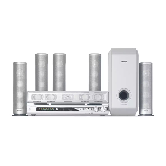
AV Receiver
Service
Service
Service
Service
Service
Service Manual
©
Copyright 2004 Philips Consumer Electronics B.V. Eindhoven, The Netherlands
All rights reserved. No part of this publication may be reproduced, stored in a retrieval system or
transmitted, in any form or by any means, electronic, mechanical, photocopying, or otherwise
without the prior permission of Philips.
Published by BB-ET0421 Service Audio Printed in The Netherlands Subject to modification
Version 1.0
TABLE OF CONTENTS
Location of PC Boards ................................................ 1-2
Versions Variation & Package .................................... 1-2
Specifications .............................................................. 1-3
Measurement Setup ................................................... 1-4
Service Aids ................................................................ 1-5
ESD & Safety Instruction ............................................ 1-6
Repair Instructions ......................................................... 2
Disassembly Instructions & Service positions .............. 3
Block & Wiring Diagram ................................................ 4
Main Board .................................................................... 5
Key/PowerSwitch Board ................................................ 6
Source+Phone Board .................................................... 7
Power Board .................................................................. 8
Tuner Board ................................................................... 9
Mechanical Exploded View & Parts List ...................... 10
Page
GB
LX710/
01
3139 785 30640
Advertisement
Table of Contents

Subscribe to Our Youtube Channel
Related Manuals for Philips LX710/01


Summary of Contents for Philips LX710/01
- Page 1 Mechanical Exploded View & Parts List ...... 10 © Copyright 2004 Philips Consumer Electronics B.V. Eindhoven, The Netherlands All rights reserved. No part of this publication may be reproduced, stored in a retrieval system or transmitted, in any form or by any means, electronic, mechanical, photocopying, or otherwise without the prior permission of Philips.
- Page 2 LOCATION OF PCB BOARDS 7CH IN Tuner Main PCB Power PCB Source+Vol Key PCB Phone VERSION VARIATION: Type/Versions LX710 Features & / 01 Board in used RDS function Grid Switch Line Cord (Detachable) Line Cord (Fixed) AC Voltage (110V~127V / 220~240V) AC Voltage (220V~240V)
-
Page 3: Specifications
SPECIFICATIONS MAIN UNIT Power Supply Rating 220-240V; 50Hz (for / 01) Power Supply Rating 110-127/ 220-240V; 50/60Hz AMPLIFIER SECTION Switchable (for / 69) Power output Power Consumption 180 W - Front 75W RMS / channel Dimensions (w x h x d) 435mm x 54mm x 388mm - Rear 75W RMS / channel... - Page 4 MEASUREMENT SETUP Tuner FM Bandpass LF Voltmeter 250Hz-15kHz e.g. PM2534 e.g. 7122 707 48001 RF Generator e.g. PM5326 S/N and distortion meter e.g. Sound Technology ST1700B Use a bandpass filter to eliminate hum (50Hz, 100Hz) and disturbance from the pilottone (19kHz, 38kHz). Tuner AM (MW,LW) Bandpass LF Voltmeter...
-
Page 5: Service Aids
SERVICE AIDS Service Tools: Universal Torx driver holder .........4822 395 91019 Torx bit T10 150mm ...........4822 395 50456 Torx driver set T6-T20 .........4822 395 50145 Torx driver T10 extended ........4822 395 50423 Compact Disc: SBC426/426A Test disc 5 + 5A ......4822 397 30096 SBC442 Audio Burn-in test disc 1kHz ....4822 397 30155 SBC429 Audio Signals disc .........4822 397 30184 Dolby Pro-logic Test Disc ........4822 395 10216... - Page 6 WAARSCHUWING WARNING Alle IC’s en vele andere halfgeleiders zijn All ICs and many other semi-conductors are gevoelig voor electrostatische ontladingen susceptible to electrostatic discharges (ESD). (ESD). Careless handling during repair can reduce life Onzorgvuldig behandelen tijdens reparatie kan drastically. de levensduur drastisch doen verminderen. When repairing, make sure that you are Zorg ervoor dat u tijdens reparatie via een connected with the same potential as the mass...
- Page 7 REPAIR INSTRUCTION...
- Page 8 REPAIR INSTRUCTION...
- Page 9 REPAIR INSTRUCTION...
- Page 10 REPAIR INSTRUCTION...
- Page 11 REPAIR INSTRUCTION...
- Page 12 REPAIR INSTRUCTION...
- Page 13 REPAIR INSTRUCTION...
- Page 14 REPAIR INSTRUCTION...
- Page 17 BLOCK DIAGRAM...
- Page 18 WIRING DIAGRAM...
-
Page 19: Table Of Contents
ES6128 INTERNAL IC DIAGRAM MAIN BOARD TABLE OF CONTENTS Internal IC Diagram ............5-1 CS4360 INTERNAL IC DIAGRAM Voltage ................5-4 Circuit Diagram (Botton Left) .......... 5-8 Circuit Diagram (Top Left) ..........5-9 Circuit Diagram (Tope Right) ........5-10 Circuit Diagram ( Bottom Right) ........5-11 PCB Layout(Component View) ........ - Page 20 PT2259 INTERNAL IC DIAGRAM CS4053BFN INTERNAL IC DIAGRAM TDA8924TH INTERNAL IC DIAGRAM M62446FP INTERNAL IC DIAGRAM...
-
Page 21: Internal Ic Diagram
CS4340 INTERNAL IC DIAGRAM TC4052BF INTERNAL IC DIAGRAM EN29F040A RT9164 INTERNAL IC DIAGRAM... - Page 22 WM8738ED INTERNAL IC DIAGRAM OPTICAL FUNCTION IC1001 (74HCU04D) PIN NO Voltage 3.3 IC1501 (74HCU04D) PIN NO Voltage 2.3 IC5001 (74HCU04D) PIN NO Voltage IC1002 (RT9164-33CLR) PIN NO Voltage IC1004 (EN29F0401-70PI) PIN NO Voltage PIN NO 21 Voltage 0.3 IC1005 (ES6128F) PIN NO Voltage 3.3 PIN NO 21...
-
Page 23: Voltage
IC1011 J(RC4558M) IC4005(RC4558M) PIN NO PIN NO Voltage Voltage IC1012(RC4558M) IC4006(RC4558M) PIN NO PIN NO Voltage Voltage IC1018 (CS4340) IC4007(RC4558M) PIN NO PIN NO Voltage Voltage IC1030 (AT24C02N) IC4008(RC4558M) PIN NO PIN NO Voltage Voltage IC1031 (IS42S16400A-6T) IC4009(RC4558M) PIN NO PIN NO Voltage 3.3 Voltage... - Page 24 IC5007 (TDA8924TH) IC1007 (CS4360) PIN NO PIN NO Voltage -26 Voltage PIN NO 21 PIN NO 21 Voltage Voltage IC4001 (TC4053BFN TOSHIBA) IC1009(RC4558M) PIN NO PIN NO Voltage -5.3 Voltage IC4002 (TC4053BFN TOSHIBA) IC1010(RC4558M) PIN NO PIN NO Voltage -5.3 Voltage IC4003 (TC4053BFN TOSHIBA) IC1011 J(RC4558M)
- Page 25 IC3005(RC4558M) IC4014 (M62446FP) PIN NO PIN NO Voltage Voltage PIN NO 21 IC3006(RC4558M) Voltage PIN NO PIN NO 41 Voltage Voltage 3.3 IC3007(RC4558M) IC4016 (PT2259) PIN NO PIN NO Voltage Voltage 3.3 IC4001 (TC4053BFN TOSHIBA) IC5001 (74HCU04D) PIN NO PIN NO Voltage -5.3 Voltage 0.4...
-
Page 26: Circuit Diagram (Botton Left)
CIRCUIT DIAGRAM - BOTTOM LEFT C101 C3013 C3084 IC3004 R3011 R3074 C102 C3014 C3085 IC3005 R3012 R3075 C103 C3015 C3086 IC3006 R3013 R3076 C104 C3016 C3087 IC3007 R3014 R3077 C105 C3018 C3088 IC902 R3015 R3078 C106 C3019 C3089 R3016 R3080 C107 C3021 C3090... -
Page 27: Circuit Diagram (Top Left)
CIRCUIT DIAGRAM - TOP LEFT D1001 R1026 R1523 D1002 R1027 R1524 FB1001 R1028 R1525 FB1002 R1031 R1526 FB1003 R1032 J 10 R1527 FB1004 R1033 J 10 R201 FB1005 R1034 I 10 R202 FB1006 R1035 I 10 R203 FB1007 R1036 I 10 R204 FB1008 R1037... -
Page 28: Circuit Diagram (Tope Right)
5-10 5-10 CIRCUIT DIAGRAM - TOP RIGHT C1 02 3 I 1 0 C4 0 14 H R 407 0 H C1 02 4 I 1 0 C4 0 73 H R 407 1 H C1 02 5 I 1 0 C4 0 74 H R 410 0 H C1 02 6... -
Page 29: Circuit Diagram - Bottom Right
5-11 5-11 CIRCUIT DIAGRAM - BOTTOM RIGHT C4022 F 10 C5032 D 14 C5123 D 13 FB5001 A 9 R4115 F 12 R5085 A 13 C4023 E 10 C5033 D 13 C5124 D 13 IC4007 F 15 R4116 F 13 R5086 E 14 C4024 E 10... -
Page 30: Pcb Layout(Component View)
5-12 5-12 PCB LAYOUT (COMPONENT VIEW) FB902 A 4 Q1502 E 5 R204 R4001 D 4 R5012 B 3 FB903 A 4 Q1503 E 5 R207 R4002 D 4 R5013 B 3 FB904 B 3 Q201 R208 R4007 C 4 R5014 D 1 FB905 A 4 Q202... -
Page 31: Pcb Layout(Copperside View)
5-13 5-13 PCB LAYOUT (COPPERSIDE VIEW) Q5005 D 2 R4067 C 4 R1011 A 5 R4068 R1012 A 5 R4069 R1013 A 5 R4072 R1014 A 5 R4085 R1015 A 5 R4096 R1016 C 5 R4098 R1038 B 5 R5004 D 3 R1044 B 5 R5007 D 3 R1045 B 5... - Page 32 5-14 5-14 ELECTRICAL PARTS LIST - MAIN BOARD ELECTRICAL PARTS LIST - MAIN BOARD MISCELLANEOUS CN201 9965 000 15862 CONNECTOR B2B-XH-A 2P L3013 9965 000 15871 CHOKE 10uH 10% C5119 9965 000 23896 CHIP CAP 560pF 100V 10% R5089 9965 000 23608 CHIP RES 22R 1/2W 5% CN5001 9965 000 19399 CONNECTOR 3P CL3962WVO...
-
Page 33: Electrical Parts List
5-15 5-15 ELECTRICAL PARTS LIST - MAIN BOARD DIODES ZD1002 4822 130 80272 DIODE ZENR 6.9-7.2V 0.5W IC1001 9965 000 23948 IC 14PIN 74HCU04D ZD3001 4822 130 34233 BZX79-B5V1 IC1002 9965 000 15887 IC 3 PIN RT9164-33CLR ZD3002 4822 130 34233 BZX79-B5V1 IC1004 9965 000 24081... - Page 34 PT6312 INTERNAL BLOCK DIAGRAM KEY / POWER SW BOARD EM78P459AM INTERNAL BLOCK DIAGRAM TABLE OF CONTENTS IC Interbnal Block Diagram ..........6-1 Circuit Diagram ..............6-3 PCB Layout Top & Bottom View ........6-4 Electrical Parts List ............6-5...
- Page 35 OPTICAL FUNCTION PT6311 INTERNAL BLOCK DIAGRAM IC201 (PT6311) PIN NO Voltage PIN NO 21 Voltage -23 PIN NO 41 Voltage -23 IC202 (PT6312) PIN NO Voltage 1.5 PIN NO 21 Voltage -26 -5.6 PIN NO 41 Voltage 4.3 IC203 (EM78P459AM) PIN NO Voltage PIN NO 21...
- Page 36 CIRCUIT DIAGRAM C201 R215 C202 R216 HNA-07SS63 C203 R217 DP201 DP202 C204 R218 HNA-10SS34 HNA-10SS34 C205 R219 C206 R220 C207 R221 C208 R222 C209 R223 C210 R224 C203 C204 C211 R225 -24V C212 R226 C202 C213 R227 100U/35V C214 R228 -24V C215 R229...
- Page 37 PCB LAYOUT VIEW C201 C236 SN201 B 6 XL201 C202 CN207 B 7 TA201 B 7 C209 DP201 A 4 TA202 B 7 C210 DP202 B 1 TA203 B 6 C211 IC204 TA204 B 7 C212 LD201 B 1 TA205 A 1 C213 RB205 A 2 TA206 B 4...
- Page 38 ELECTRICAL PARTS LIST - KEY & POWER SWITCH BOARD MISCELLANEOUS DP201 9965 000 24085 VFD 74x9MM HNA-10SS34 DP202 9965 000 24086 VFD 73.5x8.7MM HNA-07SS63 LD201 9965 000 24087 LED 3DIA WHITE DIFFUSE RD 2P SN201 9965 000 23591 IRT RECEIV IRM-2038F4 SN201 9965 000 24088 IRT RECEIVER IRM-2638F4 TA201...
- Page 39 SOURCE + PHONE BOARD TABLE OF CONTENTS Source + Phone Circuit Diagram ......7-2 Source + Phone PCB Layout ........7-2 Electrical Parts List (Source + Phone) ..... 7-3...
- Page 40 CIRCUIT DIAGRAM - SOURCE + PHONE PCB C214 C215 C217 B1 1 C218 JK501 RB2002 RB5001 VL201 VL202 PCB LAYOUT - SOURCE + PHONE PCB C214 C215 C217 C218 JK501 RB2002 RB5001 VL201 VL202...
- Page 41 ELECTRICAL PARTS LIST - SOURCE & PHONE BOARD MISCELLANEOUS 9965 000 24057 SOURCE PCB ASSY VL202 9965 000 17451 R-ENCODER L20xF7MM P=2.5MM VL201 9965 000 17793 R-ENCODER L20xF7MM P=2.5MM 9965 000 24056 PHONE PCB ASSY JK501 9965 000 24092 PHONE JACK D3.6 7P NICKEL Note : Only the parts mentioned in this list are normal service spare parts.
- Page 42 POWER BOARD (For Information only) It is not recommended for component repair on this board but to replace the board when it becomes defective. Therefore no service parts list is published in this chapter. The only service part available for replacement is: SW POWER SUPPLY ASSY 230V ....
- Page 43 CIRCUIT DIAGRAM - POWER BOARD...
- Page 44 PCB LAYOUT - POWER BOARD...
- Page 45 SAA6588T INTERNAL BLOCK DIAGRAM TUNER BOARD TABLE OF CONTENTS IC Interbnal Block Diagram ..........9-1 Circuit Diagram ..............9-2 OPTICAL FUNCTION PCB Layout Top & Bottom View ........9-3 IC001 (TEA5762H) PIN NO Electrical Parts List ............9-4 Voltage 0.4 PIN NO 21 Voltage -0.2...
- Page 46 CIRCUIT DIAGRAM ANT001D1 IC001 C002 IC002 C004 IF001 C005 IF002 C006 IF003 C007 Q001 C008 Q002 C009 Q003 Q004 C010 R001 C011 R002 C012 R003 C014 R004 C015 R005 C016 R006 C017 R007 C018 R008 C019 R009 C020 C021 R010 C022 R011 C023...
- Page 47 PCB LAYOUT VIEW ANT001A1 C037 D006 T005 C004 C037 IC001 T006 C005 C038 IF001 VC001 B2 C008 C039 IF002 VD001 B2 C009 C042 IF003 VR001 B3 C010 C043 C014 C044 L004 C017 C045 LXL1 C017 C046 Q002 C019 C047 Q003 C048 R005 C024...
- Page 48 4822 130 41198 2SC945P Q004 9965 000 14175 2SA733Q,P IC001 9965 000 23920 IC 44P TEA5762H QFP44 PHILIPS IC002 9965 000 23921 IC 20P SAA6588T SO20 PHILIPS Note : Only the parts mentioned in this list are normal service spare parts.
- Page 49 10-1 10-1 EXPLODED DRAWING...
- Page 50 9965 000 24102 RUBBER FOOT (CENTER) 9965 000 24103 GRILLE ASSEMBLY (CENTER) 9965 000 24064 RUBBER FOOT 9965 000 17046 PHILIPS LOGO 9965 000 17356 PLASTIC BRACKET 9965 000 17354 SPACER 9965 000 23653 DC FAN 12V 0.09A 4000RPM Note : Only the parts mentioned in this list are normal service...
Need help?
Do you have a question about the LX710/01 and is the answer not in the manual?
Questions and answers