Table of Contents
Advertisement
Please refer to the original service manual for:
CD Mechanism Unit (BRS12C) , Order No. PSG1303059AE
Speaker system SB-AKX800LM, SB-AKW800LM Order No. PMX1506007CE
TABLE OF CONTENTS
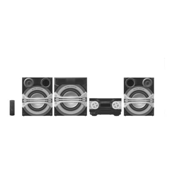
SA-AKX600LM
Model No.
SA-AKX800LM
Product Color: (K)...Black Type
© Panasonic Corporation 2015. All rights reserved.
Unauthorized copying and distribution is a violation
of law.
PMX1506006CE
CD Stereo System
Advertisement
Table of Contents


Need help?
Do you have a question about the SA-AKX600LM and is the answer not in the manual?
Questions and answers