Table of Contents
Advertisement
Please refer to the original service manual for:
CD Mechanism Unit (BRS1C), Order No. PSG1102001CE
Speaker system SB-AKX12LM-K, Order No. MEX1105004CE
Nota: El idioma original de este Manual de Servicio es en idioma inglés, sin embargo algunas notas aquí mencionadas
serán escritas en español para mejor descripción para Centros de Servicio de México.
TABLE OF CONTENTS
2.2. Precaution of Laser Diode
Model No.
Product Color: (K)...Black Type
© Panasonic Corporation 2011. All rights reserved.
Unauthorized copying and distribution is a violation
of law.
1
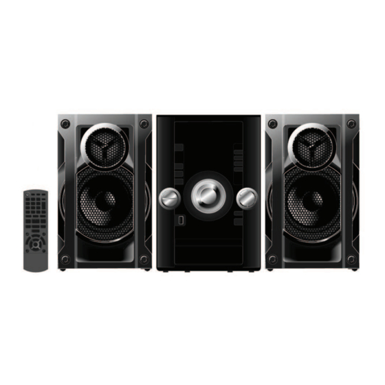
CD Stereo System
SA-AKX12LM-K
MEX1105003CE
Advertisement
Table of Contents

Related Manuals for Panasonic SA-AKX12LM-K


Summary of Contents for Panasonic SA-AKX12LM-K
-
Page 1: Table Of Contents
2.3. Service caution based on Legal restrictions 6.4. Self-Diagnostic Mode 2.4. Handling Precautions for Traverse Unit 6.5. Self-Diagnostic Error Code Table 3 Service Navigation 6.6. Sales Demonstration Lock Function © Panasonic Corporation 2011. All rights reserved. Unauthorized copying and distribution is a violation of law. - Page 2 7 Troubleshooting Guide 16.4. Panel, LCD, Remote Sensor & USB Circuit 7.1. Troubleshooting Guide for F61 and/or F76 16.5. Tuner 7.2. Part Location 16.6. SMPS Circuit 7.3. D-Amp IC Operation & Control 17 Printed Circuit Board 8 Disassembly and Assembly Instructions 17.1.
-
Page 3: Safety Precautions
1 Safety Precautions 1.1. General Guidelines 1. When servicing, observe the original lead dress. If a short circuit is found, replace all parts which have been overheated or damaged by the short circuit. 2. After servicing, see to it that all the protective devices such as insulation barriers, insulation papers shields are properly installed. -
Page 4: Before Repair And Adjustment
1.4. Before Repair and Adjustment Disconnect AC power to discharge unit AC Capacitors as such (C5700,C5701, C5703, C5704, C5705, C5708) through a 10 :, 10 W resistor to ground. Caution: DO NOT SHORT-CIRCUIT DIRECTLY (with a screwdriver blade, for instance), as this may destroy solid state devices. After repairs are completed, restore power gradually using a variac, to avoid overcurrent. -
Page 5: Safety Parts Information
1.6. Safety Parts Information Safety Parts List: There are special components used in this equipment which are important for safety. These parts are marked by in the Schematic Diagrams, Exploded View & Replacement Parts List. It is essential that these critical parts should be replaced with manufacturer’s specified parts to prevent shock, fire or other hazards. -
Page 6: Warning
2 Warning 2.1. Prevention of Electrostatic Discharge (ESD) to Electrostatic Sensitive (ES) Devices Some semiconductor (solid state) devices can be damaged easily by static electricity. Such components commonly are called Elec- trostatically Sensitive (ES) Devices. Examples of typical ES devices are integrated circuits and some field-effect transistors and semiconductor "chip"... -
Page 8: Service Caution Based On Legal Restrictions
2.3. Service caution based on Legal restrictions 2.3.1. General description about Lead Free Solder (PbF) The lead free solder has been used in the mounting process of all electrical components on the printed circuit boards used for this equipment in considering the globally environmental conservation. The normal solder is the alloy of tin (Sn) and lead (Pb). -
Page 9: Handling Precautions For Traverse Unit
2.4. Handling Precautions for Traverse Unit The laser diode in the optical pickup unit may break down due to static electricity of clothes or human body. Special care must be taken avoid caution to electrostatic breakdown when servicing and handling the laser diode in the traverse unit. Cautions to Be Taken in Handling the Optical Pickup Unit 2.4.1. - Page 10 Grounding for electrostatic breakdown prevention 2.4.2. Some devices such as the DVD player use the optical pickup (laser diode) and the optical pickup will be damaged by static electric- ity in the working environment. Proceed servicing works under the working environment where grounding works is completed. 2.4.2.1.
-
Page 11: Service Navigation
3 Service Navigation 3.1. Service Information This service manual contains technical information which will allow service personnel’s to understand and service this model. Please place orders using the parts list and not the drawing reference numbers. If the circuit is changed or modified, this information will be followed by supplement service manual to be filed with original service manual. -
Page 12: Specifications
4 Specifications ó i f i l ó i bocinas é t a í Bafle ó é t ó Potencia de salida PMPO 2800 W ó i ú ó i – ( – ( ó i Peso 87,9 MHz a 107,9 MHz (en pasos de 200 kHz) sbalanceado ó... -
Page 13: Location Of Controls And Components
5 Location of Controls and Components 5.1. Main Unit Key Button Operation Standby/on switch ( /l, POWER) Press to switch the unit from on to standby mode or vice versa.In standby mode, the unit is still consuming a small amount of power. -
Page 14: Remote Control Key Button Operation
5.2. Remote Control Key Button Operation SLEEP PLAY EXT -IN RADIO SOUND D.BASS PRESET EQ DISPLA Y DIMMER AUTO OFF... -
Page 15: Media Information
5.3. Media Information... -
Page 16: Self-Diagnostic And Special Mode Setting
6 Self-Diagnostic and Special Mode Setting 6.1. Cold-Start Here is the procedure to carry out cold-start or initialize to shipping mode. 1. Unplug AC power cord 2. Press & hold [POWER] button 3. Plug AC power cord while [POWER] button being pressed FL Display will show “_ _ _ _ _ _ _ _”... -
Page 17: Doctor Mode Table
6.2. Doctor Mode Table 6.2.1. Doctor Mode Table 1 Item Key Operation FL Display Mode Name Description Front Key Doctor Mode To enter into Doctor Mode In CD Mode: 1. Press [ ] button on main unit follow by [4] and [7] on remote control. - Page 18 6.2.2. Doctor Mode Table 2 Item Key Operation FL Display Mode Name Description Front Key Volume Setting To check the volume setting of a main In Doctor Mode: Check unit. 1. Press [7], [8], [9] button on remote control. Press [7]: VOL50 Volume Press [8]: VOL35 Press [9]: VOL0...
- Page 19 6.2.3. Doctor Mode Table 3 Item Key Operation FL Display Mode Name Description Front Key i. Function: To display result of In Doctor Mode: Self- Adjustment self-adjustment for CD. 1. Press [10] [4] button on remote control. (AJST) This is used for servicing Result Display and analysis.
-
Page 20: Reliability Test Mode (Cd Mechanism Unit (Brs1C))
6.3. Reliability Test Mode (CD Mechanism Unit (BRS1C)) Below is the process flow chart of the aging test for the CD Mechanism Unit (BRS1C). OPEN First Track Operation Access OPEN wait First Track fot 1 s Play 5 s CLOSE Last Track Operation Access... -
Page 21: Self-Diagnostic Mode
6.4. Self-Diagnostic Mode Item Key Operation FL Display Mode Name Description Front Key Self Diagnostic To enter into self diagnostic checking Step 1: Select CD mode Mode (Ensure no disc is inserted). Step 2: Press & hold [ ] follow by ] on main unit for 2 seconds. -
Page 22: Sales Demonstration Lock Function
6.5.2. CD Mechanism Error Code Table (CD Mechanism Unit (BRS1C)) Error Code Diagnostic Contents Description of error Automatic FL Display Remarks CD H15 CD Open Abnormal During operation Press [ ] on main unit for POS_SW_R On fail to be next error. -
Page 23: Troubleshooting Guide
7 Troubleshooting Guide 7.1. Troubleshooting Guide for F61 and/or F76 This section illustrates the checking procedures when upon detecting the error of “F61” and/or “F76” after power up of the unit. It is for purpose of troubleshooting and checking in SMPS & Main P.C.B. Symptom Checking Items Possible Fault(s) -
Page 24: Part Location
7.2. Part Location 7.2.1. SMPS P.C.B. AC Inlet: P5701 Fuse: Switching Regulator IC: IC5799 Switching Regulator IC: Thermistor: IC5701 TH5860 Photocoupler: PC5702, PC5799 Rectifier Diode D5801, D5802 Photocoupler: PC5720 Connector: Transformer: CN5802 T5701 Fig. 1 SMPS P.C.B. - Page 25 7.2.2. Main P.C.B. Audio Digital Amp IC: IC5902 Cable wire: ZJ2002 Voltage Regulator IC: IC2010 Switching Regulator IC: IC2011 Fig. 2 Main P.C.B.
-
Page 26: D-Amp Ic Operation & Control
7.3. D-Amp IC Operation & Control... - Page 27 1170 ~ 1250 1260 ~ 1450 1460 ~ 1540 1550 ~ 1710 Table 4: F_HOP Control during 10 kHz Step Note: During activating, the 3 control pins namely MUTE_F, MUTE_A and MODE_DA must be used to cover the “Pop” sound cause by F-HOP switching.
-
Page 28: Disassembly And Assembly Instructions
8 Disassembly and Assembly Instructions • Illustration is based on SA-AKX12PH-K. Caution Note: • This section describes the disassembly and/or assembly procedures for all major printed circuit boards & main compo- nents for the unit. (You may refer to the section of “Main components and P.C.B Locations” as described in the service manual) •... -
Page 29: Disassembly Flow Chart
8.1. Disassembly Flow Chart 8.3. Top Cabinet 8.20. CD Mechanism Unit 8.4. Tuner P.C.B. 8.11. Main P.C.B. (BRS1C) 8.5. Front Panel 8.21. Rear Panel 8.12. Voltage Regulator Unit IC (IC2010) 8.22. Voltage Selector P.C.B. 8.13. Audio Digital Amp 8.6. Panel P.C.B. IC (IC5902) 8.7. -
Page 30: Main Components And P.c.b. Locations
8.2. Main Components and P.C.B. Locations... -
Page 31: Disassembly Of Top Cabinet
8.3. Disassembly of Top Cabinet Step 4 Slightly lift up both side of Top Cabinet in an outward direction as shown. Step 1 Remove 2 screws on each side. Step 5 Remove Top Cabinet. Step 2 Remove 5 screws. Step 3 Slightly pull both side of Top Cabinet outwards as arrow shown. -
Page 32: Disassembly Of Tuner P.c.b
8.4. Disassembly of Tuner P.C.B. 8.5. Disassembly of Front Panel • Refer to “Disassembly of Top Cabinet”. Unit • Refer to “Disassembly of Top Cabinet”. Step 1 Remove 1 screw. Step 1 Detach 17P FFC at the connector (CN2003) on Main P.C.B. - Page 33 Step 4 Release tabs at bottom. Step 6 Remove Front Panel Unit Step 5 Push inwards slightly at the Bottom Chassis and release tab at right side of Front Panel Unit.
-
Page 34: Disassembly Of Panel P.c.b
8.6. Disassembly of Panel P.C.B. Step 4 Release catches by following the sequences (1-3). • Refer to “Disassembly of Top Cabinet”. • Refer to “Disassembly of Front Panel Unit”. Step 1 Remove the Volume Knob. Step 2 Remove the Track Knob. Step 5 Remove the Panel P.C.B. -
Page 35: Disassembly Of Remote Sensor P.c.b
8.7. Disassembly of Remote Sensor Step 6 Desolder 7 pins at (ZJ600B) on Panel P.C.B.. Step 7 Remove the Panel P.C.B.. P.C.B. • Refer to “Disassembly of Top Cabinet”. • Refer to “Disassembly of Front Panel Unit”. • Refer to (Step 1) to (Step 5) of item 9.6.. Step 1 Remove Remote Sensor P.C.B.. -
Page 36: Disassembly Of Lcd P.c.b
8.8. Disassembly of LCD P.C.B. Caution: During assembling, ensure that LCD Unit is prop- erly located & seated onto the guides. • Refer to “Disassembly of Top Cabinet”. • Refer to “Disassembly of Front Panel Unit”. Step 1 Remove 2 screws. Step 2 Lift up LCD Unit. -
Page 37: Disassembly Of Usb P.c.b
8.9. Disassembly of USB P.C.B. 8.10. Disassembly of CD Lid • Refer to “Disassembly of Top Cabinet”. • Refer to “Disassembly of Top Cabinet”. • Refer to “Disassembly of Front Panel Unit”. • Refer to “Disassembly of Front Panel Unit”. Step 1 Remove 2 screws. -
Page 38: Disassembly Of Main P.c.b
8.11. Disassembly of Main P.C.B. Step 3 Remove 2 screws. Step 4 Detach Main P.C.B. from Rear Panel according to arrow • Refer to “Disassembly of Top Cabinet”. shown. • Refer to “Disassembly of Front Panel Unit”. Step 1 Detach 15P Cable Wire at the connector (CN5802) on SMPS P.C.B.. -
Page 39: Replacement Of Voltage Regulator Ic (Ic2010)
8.12. Replacement of Voltage Regu- Step 5 Detach 27P FFC at the connector (CN2706) on Main P.C.B.. lator IC (IC2010) Step 6 Detach 9P FFC at the connector (CN2010) on Main P.C.B.. • Refer to “Disassembly of Main P.C.B.”. Step 7 Remove Main P.C.B.. 8.12.1. -
Page 40: Replacement Of Audio Digital Amp Ic
8.13. Replacement of Audio Digital 8.12.2. Assembly of Voltage Regulator IC (IC2010) Amp IC (IC5902) Step 1 Apply grease to the Heatsink. • Refer to “Disassembly of Main P.C.B.”. Step 2 Fix the Voltage Regulator IC (IC2010) on Main P.C.B.. 8.13.1. -
Page 41: (Ic5902)
Step 3 Remove Heatsink Clip. Step 4 Solder pins of the Audio Digital Amp IC (IC5902) on the Step 4 Remove Audio Digital Amp IC (IC5902). solder side of Main P.C.B.. 8.13.2. Assembly of Audio Digital Amp IC (IC5902) Step 1 Apply grease to the Heatsink. Step 2 Fix the Audio Digital Amp IC (IC5902) on Main P.C.B. -
Page 42: Disassembly Of Smps P.c.b
8.14. Disassembly of SMPS P.C.B. Step 4 Flip the SMPS P.C.B. and position it according to dia- gram shown. • Refer to “Disassembly of Top Cabinet.”. Step 5 Place SMPS P.C.B. on an insulated material. • Refer to “Disassembly of Front Panel Unit”. Step 6 Desolder 2 Wire pins, TL7 (Black), TL8 (Red) wires pin. -
Page 43: Replacement Of Switching Regulator Ic (Ic5701)
8.15. Replacement of Switching Reg- Step 2 Remove 1 screw. Step 3 Remove the Switching Regulator IC (IC5701). ulator IC (IC5701) Caution: Avoid touching the Heatsink A due to its high temperature after prolonged use. Touching it may lead to •... -
Page 44: Replacement Of Rectifier Diode (D5702)
8.16. Replacement of Rectifier Diode Step 4 Solder pins of the Switching Regulator IC (IC5701) on the solder side of SMPS P.C.B.. (D5702) • Refer to “Disassembly of SMPS P.C.B.”. 8.16.1. Disassembly of Rectifier Diode (D5702) Step 1 Desolder pins of the Rectifier Diode (D5702) on the sol- der side of SMPS P.C.B. - Page 45 Step 3 Remove 1 screw at Switching Regulator IC (IC5701). 8.16.2. Assembly of Rectifier Diode Step 4 Remove the Heatsink A with Rectifier Diode (D5702). (D5702) Step 5 Remove 1 screw. Step 1 Apply grease to the Heatsink A. Step 6 Remove the Rectifier Diode (D5702) from the Heatsink Step 2 Screw the Rectifier Diode (D5702) to the Heatsink A.
-
Page 46: Replacement Of Rectifier Diode (D5801)
8.17. Replacement of Rectifier Diode Step 5 Solder pins of the Rectifier Diode (D5702) on the solder side of SMPS P.C.B.. (D5801) Step 6 Solder pins of the Heatsink A on the solder side of SMPS P.C.B.. • Refer to “Disassembly of SMPS P.C.B.”. Caution: Ensure pins of the Rectifier Diode (D5702) are properly seated and soldered on SMPS P.C.B.. -
Page 47: Replacement Of Rectifier Diode (D5802)
8.18. Replacement of Rectifier Diode 8.17.2. Assembly of Rectifier Diode (D5801) (D5802) Step 1 Apply grease to the Heatsink B. • Refer to “Disassembly of SMPS P.C.B.”. Step 2 Fix the Rectifier Diode (D5801) on SMPS P.C.B. Caution: Ensure pins of the Rectifier Diode (D5801) is properly inserted on SMPS P.C.B. -
Page 48: Replacement Of Regulator Diode (D5803)
8.19. Replacement of Regulator 8.18.2. Assembly of Rectifier Diode (D5802) Diode (D5803) Step 1 Apply grease to the Heatsink B. • Refer to “Disassembly of SMPS P.C.B.”. Step 2 Fix the Rectifier Diode (D5802) on SMPS P.C.B.. Caution: Ensure pins of the Rectifier Diode (D5802) is properly inserted on SMPS P.C.B. -
Page 49: Disassembly Of Cd Mechanism Unit (Brs1C)
8.20. Disassembly of CD Mecha- 8.19.2. Assembly of Rectifier Diode (D5803) nism Unit (BRS1C) Step 1 Apply grease to the Heatsink B. • Refer to “Disassembly of Top Cabinet”. Step 2 Fix Rectifier Diode (D5803) on SMPS P.C.B. • Refer to “Disassembly of Front Panel Unit”. Caution: Ensure pins of the Rectifier Diode (D5803) are properly inserted on SMPS P.C.B. - Page 50 Step 3 Remove 3 screws. Step 5 Lift up and remove SMPS Inner Chassis Unit. Caution: During assembling, ensure that SMPS Inner Chassis is catched onto Rear Panel properly. Step 4 Detach Voltage Selector P.C.B. from Rear Panel as arrow shown.
-
Page 51: Disassembly Of Rear Panel
8.21. Disassembly of Rear Panel Step 6 Remove 2 screws. • Refer to “Disassembly of Top Cabinet”. • Refer to “Disassembly of Tuner P.C.B.”. Step 1 Remove 8 screws. Step 2 Detach Voltage Selector P.C.B. from Rear Panel as arrow shown. Step 7 Lift up &... - Page 52 Step 3 Step 4 Step 5...
-
Page 53: Replacement Of Traverse Unit
9 Replacement of Traverse Unit 9.1. Disassembly of Traverse Unit Step 2: Slide the tray out fully. • Refer to “Disassembly of CD Mechanism Unit (BRS1C)”. Caution: Refer to “2.4 Handling Precaution for Traverse Unit” to prevent static damage to the Optical Pickup Unit. Note: 1. - Page 54 Step 4: Release the guide as shown & slide the Traverse Slide Step 6: Lift the Traverse Unit by approximately 45q. Plate to the end. Step 7: Slide out the traverse unit as arrow shown. Step 5: Detach 5P FFC at the connector (CN7003) on CD Servo P.C.B..
-
Page 55: Assembly Of Traverse Unit
9.2. Assembly of Traverse Unit Step 2: Slot the Traverse Unit at approximately 45q into the mecha chassis as arrow shown. Step 1: Release the guide as shown & slide the Traverse Slide Plate to the end. - Page 56 Step 3: Ensure the Traverse Unit seated properly onto the Step 6: Slide the Traverse Slide Plate unit it stop at the Guide. Groove. Step 7: Slot the Tray into the guides as Picture shown. Step 4: Slide Traverse Slide Plate to lock the Traverse Unit as shown.
-
Page 57: Disassembly Of Cd Servo P.c.b
9.3. Disassembly Servo Step 8: Ensure the guides is align with the groove when sliding the tray in. P.C.B. • Refer to “Disassembly of CD Mechanism Unit (BRS1C)”. • Refer to “Replacement of Traverse Unit”. Caution: It is required to short the circuit. Step 1: Solder the 3 solder points. - Page 58 Caution 2: During assembling, desolder the solder points. Step 5 Slightly lift up the CD Servo P.C.B. Step 6 Flip the CD Servo P.C.B. Step 2 Remove 3 screws. Step 3 Desolder 4 pins. Step 4 Detach 5P FFC at the connector (CN7003) on CD Servo P.C.B..
- Page 59 Step 9 Ground the 24P FFC with a short pin.
-
Page 60: Service Position
10 Service Position 10.2. Checking and Repairing of Panel P.C.B. Note: For description of the disassembly procedures, see the Section 9. Step 1 Remove Top Cabinet. Step 2 Remove Front Panel Unit. 10.1. Checking and Repairing of Step 3 Attach 5P Cable Wire to the connector (CN1113) on Main P.C.B. - Page 61 10.3. Checking and Repairing of LCD 10.4. Checking and Repairing of P.C.B. SMPS P.C.B. Step 1 Remove Top Cabinet. Step 1 Remove Top Cabinet. Step 2 Remove Front Panel Unit. Step 2 Remove Front Panel Unit. Step 3 Position LCD Unit on the insulated material as shown. Step 3 Remove SMPS P.C.B..
-
Page 62: Checking And Repairing Of Cd Servo P.c.b
10.5. Checking and Repairing of CD Servo P.C.B. Step 1 Remove Top Cabinet. Step 2 Remove Front Panel Unit. Step 3 Remove SMPS Chassis Unit. Step 4 Remove CD Mechanism Unit (BRS1C). Step 5 Position Front Panel Unit, SMPS Chassis Unit as dia- gram shown. -
Page 63: Voltage & Waveform Chart
11 Voltage & Waveform Chart Note: • Indication Voltage Values are in standard values for the unit measured by the DC electronic circuit tester (high-impedance) with the chassis taken as standard. Therefore, there may exist some errors in voltage values, depending on the internal impedance of the DC circuit tester. •... - Page 64 11.2. Main P.C.B. (1/2) IC2003 REF NO. MODE POWER ON STANDBY REF NO. IC2003 MODE POWER ON 3.2 STANDBY IC2003 REF NO. MODE POWER ON STANDBY IC2003 REF NO. MODE POWER ON STANDBY IC2003 REF NO. MODE POWER ON 3.3 STANDBY IC2006 REF NO.
- Page 65 11.3. Main P.C.B. (2/2) REF NO. IC2101 MODE CD PLAY STANDBY IC2101 REF NO. MODE CD PLAY STANDBY IC2201 REF NO. MODE CD PLAY 12.0 STANDBY 12.0 IC5902 REF NO. MODE CD PLAY 35.1 -35.1 -26.7 35.4 16.8 -35.3 -25.3 -35.3 17.0 35.4 -35.1 -35.1 35.0 STANDBY...
-
Page 66: Lcd P.c.b
11.4. LCD P.C.B. IC900 REF NO. MODE POWER ON 3.3 STANDBY IC900 REF NO. MODE POWER ON 1.4 STANDBY IC900 REF NO. MODE POWER ON 1.4 STANDBY Q900 REF NO. MODE POWER ON STANDBY SA-AKX12 LCD P.C.B. 11.5. Tuner P.C.B. IC52 REF NO. -
Page 67: Smps P.c.b
11.6. SMPS P.C.B. IC5701 REF NO. MODE POWER ON 164.8 19.1 STANDBY 164.8 19.1 IC5799 REF NO. MODE POWER ON 5.9 11.0 164.2 STANDBY 11.0 164.2 REF NO. IC5801 MODE POWER ON 2.4 -30.0 STANDBY -30.0 IC5899 REF NO. MODE POWER ON 1.2 STANDBY Q5720... -
Page 68: Waveform Table
11.7. Waveform Table 0.1Vp-p(200usec/div) 0.2Vp-p(100usec/div) 2Vp-p(10usec/div) 3Vp-p(20usec/div) 3.6Vp-p(200usec/div) 1.4Vp-p(1msec/div) 0.1Vp-p(200usec/div) 1.3Vp-p(200usec/div) 100Vp-p(1usec/div) 1.5Vp-p(500usec/div) -
Page 69: Illustration Of Ics, Transistor And Diode
12 Illustration of ICs, Transistor and Diode Este material se encuentra sin programar, debe se programado. MN101EF16KXW C1BB00001151 (32P) C0HBA0000295 (44P) C3EBFY000006 (8P) C1BA00000497 (23P) VUEALLPT031 (100P) (20P) No.1 No.1 No.1 No.1 MN6627947RB C0GBY0000117 C0AABB000125 (8P) MIP2F20MSSCF (8P) C0DBFYY00049 C3EBFC000042 (144P) No.1 C0DAAYG00001 (5P) -
Page 76: Schematic Diagram
16 Schematic Diagram • For PH only 16.1. Schematic Diagram Notes • This schematic diagram may be modified at any time with the development of new technology. Notes: S5701: Voltage ADJ switch (For PH only). S6001: Power switch ( S6002: USB switch. - Page 91 18.2. IC900(C0HBA0000295): IC FL Driver Terminal Name Function Chip Selection Input Read Clock Input Write Clock Input DATA I/O Serial Data Input Negative Power Supply VLCD LCD Power Input Positive Power Supply O Tone Frequency Output Pair COM0 O Common Output 0 COM1 O Common Output 1 COM2...
- Page 98 Lista de Materiales Eléctricos Safety Ref. No. Part No. Part Name & Description K5D802APA008 FUSIBLE RAIM11X120A CONJUNTO SMPS AKX12 REPM11X120A CONJUNTO MANUAL SMPS AKX12 C5727 F1B3A3320012 CAPACITOR C5708 F1BAF1020020 CAPACITOR C5805 F2A1H1020067 CAPACITOR C5808 F2A1H1020067 CAPACITOR C5701 F0CAF104A105 CAPACITOR C5700 F1BAF471A013 CHIP CAPACITOR C5703...
- Page 99 Q5862 B1GBCFJJ0051 TRANSISTOR R5724 ERJ6GEYJ121V R.CHIP R5703 D0GZ333JA012 CHIP RESISTOR R5729 ERJ6GEYJ103V R.CHIP R5721 ERJ6GEYJ103V R.CHIP R5797 ERJ3GEYJ153V RESISTENCIA CHIP PEL CULA R5805 ERJ3RBD222V PRESICION CHIP RESISTOR R5806 ERJ3GEYJ153V RESISTENCIA CHIP PEL CULA R5730 ERJ3GEYJ102V CHIP RESISTOR R5723 ERJ3GEYJ102V CHIP RESISTOR R5705 ERJ8GEYJ224V CHIP RESISTOR...
- Page 100 W5535 Z-W6NL ALAMBRE JUMPER W5520 Z-W6NL ALAMBRE JUMPER W5514 Z-W6NL ALAMBRE JUMPER W5516 Z-W6NL ALAMBRE JUMPER W5508 Z-W6NL ALAMBRE JUMPER W5512 Z-W6NL ALAMBRE JUMPER W5506 Z-W6NL ALAMBRE JUMPER W5509 Z-W6NL ALAMBRE JUMPER W5505 Z-W6NL ALAMBRE JUMPER W5510 Z-W6NL ALAMBRE JUMPER W5526 Z-W6NL ALAMBRE JUMPER...
- Page 101 CN1113 K1KA05BA0061 CONECTOR 5 PIN K2AA28000017 CONECTOR TOMACORRIENTE JK1111 K1FY104B0011 CONECTOR JK2000 K2HA204B0153 2 PIN RCA JACK HL600 RMXX1008-1 LCD diffuser IR6000 B3RAB0000084 SENSOR PARA CONTRO REMOTO D993 B3AFA0000131 IC2010 C0CAAKG00046 IC REGULADOR IC2201 C0AABB000125 OP AMP IC IC5902 C1BA00000497 D-AMP IC Z900 L5AYAYY00061...
- Page 102 C2157 F1J0J106A020 CHIP CAPACITOR C5800 F1H1H104A013 CHIP CAPACITOR C5802 F1H1H104A013 CHIP CAPACITOR C2224 F1H1A224A007 CHIP CAPACITOR C5803 F1H1H104A013 CHIP CAPACITOR C2204 F1H1H470A004 CHIP CAPACITOR C2144 F1H0J1050012 CHIP CAPACITOR C5801 F1H1H104A013 CHIP CAPACITOR C2191 F1H1H103A219 CHIP CAPACITOR C2142 F1H1C104A042 CHIP CAPACITOR C2246 F1H1C104A042 CHIP CAPACITOR...
- Page 103 IC2003 MN101EF16KXW IC MICROP VE IC2009 C0DBFYY00049 ICs For Power Supply IC2006 C3EBFY000006 EEPROM D2025 D0GBR00JA008 CHIP JUMPER DZ2000 B0JCPD000025 DIODE D5908 B0HCSP000001 CHIP DIODO Q2220 B1ABCF000176 TRANSISTOR Q2041 B1ABCF000176 TRANSISTOR Q2040 B1ABCF000176 TRANSISTOR Q2039 B1ADCE000012 TRANSISTOR Q2050 B1ADCE000012 TRANSISTOR Q2014 B1GBCFLL0037 CHIP TRANSISTOR...
- Page 104 R2196 ERJ3GEYJ102V CHIP RESISTOR R2156 ERJ3GEYJ101V CHIP RESISTOR R2159 ERJ3GEYJ101V CHIP RESISTOR R2214 ERJ3GEYJ102V CHIP RESISTOR R2201 ERJ3GEYJ102V CHIP RESISTOR R2198 ERJ3GEYJ102V CHIP RESISTOR R2185 ERJ3GEYJ103V CHIP RESISTOR R2218 D0GB103JA008 CHIP RESISTOR R2219 ERJ3GEYJ222V CHIP RESISTOR R2197 ERJ3GEYJ101V CHIP RESISTOR R2233 ERJ3GEYJ272V RESISTENCIA CHIP PEL CULA...
- Page 105 R5947 ERJ1TYJ220U CHIP RESISTOR R6058 ERJ3GEYJ123V RESISTENCIA CHIP PEL CULA R6067 ERJ3GEYJ123V RESISTENCIA CHIP PEL CULA R6010 ERJ3GEYJ472V RESISTENCIA CHIP PEL CULA R903 D0GB471JA008 CHIP RESISTOR R6005 ERJ3GEYJ472V RESISTENCIA CHIP PEL CULA R6003 ERJ3GEYJ222V CHIP RESISTOR R6012 ERJ3GEYJ103V CHIP RESISTOR R5951 ERJ3GEYJ562V CHIP RESISTOR...
- Page 106 S6009 EVQ21405RJ TACK SWITCH S6008 EVQ21405RJ TACK SWITCH RENM11X121AZ CONJUNTO AXIAL D-AMP/ MAIN/PANEL/ USB A RENM11X121AJ CONJUNTO JUMPER D-AMP/ MAIN/PANEL/ USB RJBX0728A PCB MAIN-PANEL-D-AMP- USB K2001 Z-W6NL ALAMBRE JUMPER K2018 Z-W6NL ALAMBRE JUMPER K2020 Z-W6NL ALAMBRE JUMPER K2013 Z-W6NL ALAMBRE JUMPER K2021 Z-W6NL ALAMBRE JUMPER...
- Page 107 W5044 Z-W6NL ALAMBRE JUMPER W5040 Z-W6NL ALAMBRE JUMPER W5074 Z-W6NL ALAMBRE JUMPER W5070 Z-W6NL ALAMBRE JUMPER W5064 Z-W6NL ALAMBRE JUMPER W5059 Z-W6NL ALAMBRE JUMPER W5062 Z-W6NL ALAMBRE JUMPER W5071 Z-W6NL ALAMBRE JUMPER W5063 Z-W6NL ALAMBRE JUMPER W5066 Z-W6NL ALAMBRE JUMPER W5069 Z-W6NL ALAMBRE JUMPER...
- Page 108 C2120 F1H1H122A219 CHIP CAPACITOR C2121 F1H1H472A219 CHIP CAPACITOR C2131 F1H1H122A219 CHIP CAPACITOR C2225 D0GBR00JA008 CHIP JUMPER C5922 D0GBR00JA008 CHIP JUMPER K1210 D0GBR00JA008 CHIP JUMPER QR2400 B1GDCFJJ0047 TRANSISTOR QR2402 B1GDCFJJ0047 TRANSISTOR R2003 ERJ3GEY0R00V CHIP JUMPER R2004 ERJ3GEY0R00V CHIP JUMPER R2015 ERJ3GEYJ473V RESISTENCIA CHIP PEL CULA R2016 ERJ3GEYJ473V...
Need help?
Do you have a question about the SA-AKX12LM-K and is the answer not in the manual?
Questions and answers