Table of Contents
Advertisement
SERVICE MANUAL
Ver. 1.1 2007. 08
Sony Corporation
9-887-769-02
2007H04-1
eVehicle Division
© 2007. 08
Published by Sony Techno Create Corporation
Photo: Red Logo
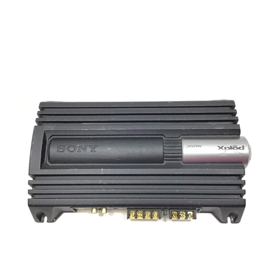
SPECIFICATIONS
Circuit system
OTL (output transformerless) circuit
Pulse power supply
Inputs
RCA pin jacks
High level input connector
Input level adjustment range
0.3 – 6 V (RCA pin jacks),
2.8 – 12 V (High level input)
Outputs
Speaker terminals
Speaker impedance
2 – 8 Ω (stereo)
4 – 8 Ω (when used as a bridging amplifier)
110 W × 2 (at 4 Ω)
Maximum outputs
350 W (BTL, at 4 Ω)
Rated outputs (supply voltage at 14.4 V)
60 W × 2 (20 Hz – 20 kHz, 1% THD, at 4 Ω)
65 W × 2 (20 Hz – 20 kHz, 0.1% THD, at 2 Ω)
130 W (BTL) (20 Hz – 20 kHz, 0.1% THD, at 4 Ω)
Frequency response
5 Hz – 50 kHz (
0.005% or less (at 1 kHz, 4 Ω)
Harmonic distortion
Low-pass filter
80 Hz, –18 dB/oct
Power requirements
12 V DC car battery (negative ground)
Power supply voltage
10.5 – 16 V
Current drain
at rated output : 15 A (at 4 Ω, 60 W × 2)
Remote input : 1 mA
Dimensions
Approx. 321 × 55 × 200 mm (w/h/d)
not incl. projecting parts and controls
Mass
Approx. 2.0 kg not incl. accessories
Supplied accessories
Mounting screws (4)
High level input cord (1)
Protection cap (1)
Design and specifications are subject to change without
notice.
XM-ZR602
+0
dB)
–3
STEREO POWER AMPLIFIER
AEP Model
UK Model
E Model
1
Advertisement
Table of Contents

Related Manuals for Sony XM-ZR602


Summary of Contents for Sony XM-ZR602
-
Page 1: Service Manual
Supplied accessories Mounting screws (4) High level input cord (1) Protection cap (1) Design and specifications are subject to change without notice. STEREO POWER AMPLIFIER Sony Corporation 9-887-769-02 2007H04-1 eVehicle Division © 2007. 08 Published by Sony Techno Create Corporation... -
Page 2: Table Of Contents
WITH MARK 0 ON THE SCHEMATIC DIAGRAMS AND IN THE PARTS LIST ARE CRITICAL TO SAFE OPERATION. REPLACE THESE COMPONENTS WITH SONY PARTS WHOSE PART NUMBERS APPEAR AS SHOWN IN THIS MANUAL OR IN SUPPLEMENTS PUBLISHED BY SONY. -
Page 3: General
El representante autorizado para la aplicación de la manipulación en el momento de deshacerse de este LEVEL directiva EMC y la seguridad de los productos es Sony producto. El reciclaje de materiales ayuda a conservar Deutschland GmbH, Hedelfinger Strasse 61, 70327 los recursos naturales. -
Page 4: Power Connection
XM-ZR602 Connections/Conexiones/ Make the terminal connections as illustrated below. Realice las conexiones de terminal como se ilustra a continuación. Ligações Ligue os terminais como se mostra na figura abaixo. Installation RE M Before Installation First, place the unit where you plan to install it, and... -
Page 5: Speaker Connections
XM-ZR602 Input Connections/Conexiones de entrada/Ligações de entrada Speaker Connections Turn on or off the LPF switch at the unit rear as illustrated below. Line Input Connection (with Speaker Connection 1, 2 or 4) Conexiones de los altavoces Conexión de entrada de línea (con conexión de altavoces 1, 2 ó 4) Ligação de entrada de linha (com ligação às colunas 1, 2 ou 4) - Page 6 XM-ZR602 Dimensions/Dimensiones/Dimensões Table of crossover values for 6 dB/octave Notes • When using passive crossover networks in a multi- (4 Ω) (Speaker Connections 4) speaker system, care must be taken as the speaker Unit: mm system’s impedance should not be lower than that of...
-
Page 7: Disassembly
XM-ZR602 SECTION 2 DISASSEMBLY Note : This set can be disassemble according to the following sequence. 2-1. BOTTOM PLATE (Page 7) 2-2. MAIN BOARD SECTION (Page 8) 2-3. MAIN BOARD (Page 8) Note : Follow the disassembly procedure in the numerical order given. - Page 8 XM-ZR602 2-2. MAIN BOARD SECTION 1 three screws (+P 3 × 8) 2 three screws (+P 3 × 8) 3 three screws (+P 3 × 8) 4 MAIN board section main heat sink 2-3. MAIN BOARD 5 MAIN board 4 front panel 3 screw (+P 3 ×...
-
Page 9: Diagrams
XM-ZR602 SECTION 3 DIAGRAMS 3-1. BLOCK DIAGRAM PRE AMP IC301 (1/2) CNJ901 L.P.F GAIN CONTROL AMP IC302 (1/2) IC303 (1/2) SWITCH (BTL) CN903 (1/2) Q101 POWER DIFFERENTIAL DRIVE DRIVE FILTER INPUT Q110 Q103 Q104 Q108 VR301-1 SW301-1 D906 CN901 BIAS... - Page 10 XM-ZR602 • Note for Replacement of the Transistors • Waveform THIS NOTE IS COMMON FOR PRINTED WIRING The transistors Q110, 111, 210 and 211 have two different ranks: P BOARDS AND SCHEMATIC DIAGRAMS. rank and Y rank. (In addition to this, the necessary note is IC901 5 printed in each block.)
-
Page 11: Printed Wiring Board
XM-ZR602 3-2. PRINTED WIRING BOARD : Uses unleaded solder. • Semiconductor Location Ref. No. Location D101 D102 D201 D202 D301 D302 D303 B-10 D304 C-10 D305 D306 D307 B-10 D902 D903 D904 D905 D906 D918 IC301 IC302 IC303 IC901 IC902... -
Page 12: Schematic Diagram
XM-ZR602 3-3. SCHEMATIC DIAGRAM • Refer to page 10 for Waveform and page 13 for IC Block Diagram. D101 R122 R118 R121 R138 Q104 Q108 R133 C112 R128 C117 R104 Q112 Q110 R130 R101 R126 C116 R105 R124 Q103 R943... -
Page 13: Ic Block Diagram
XM-ZR602 • IC Block Diagram IC901 TL594INSR REF 5V ERROR ERROR 0.1V... -
Page 14: Exploded Views
XM-ZR602 SECTION 4 EXPLODED VIEWS NOTE: • The mechanical parts with no reference • Color Indication of Appearance Parts The components identified by mark 0 or dotted line with mark number in the exploded views are not supplied. Example : 0 are critical for safety. -
Page 15: Main Board Section
XM-ZR602 4-2. MAIN BOARD SECTION not supplied not supplied Q111,Q110 Q210,Q211 not supplied D304,D303 Q910,Q911 Ref. No. Part No. Description Remark Ref. No. Part No. Description Remark A-1283-682-A MAIN BOARD, COMPLETE Q111 8-729-024-76 TRANSISTOR 2SA1908-P 3-225-184-12 SCREW (+PS.TT.3XL) Q111 8-729-024-77 TRANSISTOR 2SA1908-Y... -
Page 16: Electrical Parts List
XM-ZR602 SECTION 5 MAIN ELECTRICAL PARTS LIST NOTE: • Due to standardization, replacements in • SEMICONDUCTORS The components identified by mark 0 or dotted line with mark the parts list may be different from the In each case, u : µ, for example: 0 are critical for safety. - Page 17 XM-ZR602 MAIN Ref. No. Part No. Description Remark Ref. No. Part No. Description Remark < DIODE > Q207 8-729-026-49 TRANSISTOR 2SA1037AK-T146-R Q208 8-729-020-80 TRANSISTOR 2SC2235-O/Y(TPE6) D101 8-719-988-61 DIODE 1SS355TE-17 Q209 8-729-232-32 TRANSISTOR 2SA965 D102 8-719-988-61 DIODE 1SS355TE-17 Q210 8-729-024-79 TRANSISTOR 2SC5100-P...
- Page 18 XM-ZR602 MAIN Ref. No. Part No. Description Remark Ref. No. Part No. Description Remark R126 1-218-843-11 METAL CHIP 0.5% 1/10W R306 1-216-222-00 RES-CHIP 1/8W R127 1-218-831-11 METAL CHIP 0.5% 1/10W R307 1-216-210-00 RES-CHIP 3.3K 1/8W R128 1-216-837-11 METAL CHIP 1/10W...
- Page 19 XM-ZR602 MAIN Ref. No. Part No. Description Remark < THERMISTOR > TH901 1-801-597-11 THERMISTOR TH902 1-801-597-11 THERMISTOR TH903 1-801-597-11 THERMISTOR < VARIABLE RESISTOR > VR301 1-227-768-11 RES, VAR, CARBON 10KX2 (LEVEL) ************************************************************* ACCESSORIES ************ 3-215-703-11 MANUAL, INSTRUCTION (ENGLISH,SPANISH, PORTUGUESE) 3-215-703-21 MANUAL, INSTRUCTION (FRENCH,GERMAN,...
- Page 20 XM-ZR602 REVISION HISTORY Clicking the version allows you to jump to the revised page. Also, clicking the version at the top of the revised page allows you to jump to the next revised page. Ver. Date Description of Revision 2007. 07 2007.
Need help?
Do you have a question about the XM-ZR602 and is the answer not in the manual?
Questions and answers