Table of Contents

Advertisement

Specification
n Amplifier Section
Power output
10%, Total harmonic distortion
60 Hz-3 kHz, both channels driven
(Low channel)
3 kHz-16 kHz, both channels driven
(High channel)
Total Bi-Amp power
Power output
10% Total harmonic distortion
1 kHz, both channels driven
(Low channel)
8 kHz, both channels driven
(High channel)
Total Bi-Amp power
Output Impedance
Headphone
n FM Tuner Section
Frequency range
Sensitivity
S/N 26dB
Antenna terminal(s)
n AM Tuner Section
Frequency range
26 W per channel (6 Ω)
29 W per channel (6 Ω)
55 W per channel
35 W per channel (6 Ω)
70 W per channel
16Ω - 32 Ω
87.5 MHz - 108.0 MHz
(100 kHz steps)
87.9 MHz - 107.9 MHz
(200 kHz steps)
1.5 µV (IHF)
1.5 µV
75 Ω (unbalanced)
520kHz - 1710 kHz (10kHz steps)
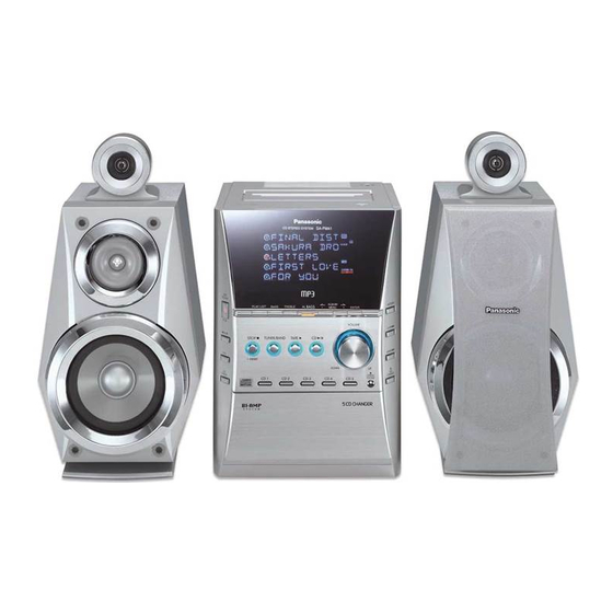
SA-PM41P
SA-PM41PC
Colour
(S)... Silver Type
Sensitivity
S/N 20 dB (at 1000 kHz)
n Cassette Deck Section
Track system
Heads
Record/playback
Erasure
Motor
Recording system
Erasing system
Tape speed
Overall frequency response (+3 dB, -6 dB) at DECK OUT)
NORMAL (TYPE I)
S/N RATIO
Wow and flutter
Fast forward and rewind time
n CD Section
Disc
CD, CD-R, CD-RW, MP3
Sampling frequency
Decoding
Beam source / wavelength
Number of channels
Frequency response
Wow and flutter
Digital filter
© 2005 Matsushita Electric Industrial Co. Ltd.. All
rights
reserved.
distribution is a violation of law.
ORDER NO. MD0501004C1
CD Stereo System
560 µV/m
4 track, 2 channel
Solid permalloy head
Double gap ferrite head
DC servo motor
AC bias 100 kHz
AC erase 100 kHz
35 Hz - 14 kHz
45dB (A weighted)
0.10% (WRMS)
Approx. 120 seconds with C-60
cassette tape
3
8cm / 12cm (3
/
" / 4
20
44.1 kHz
16 bit linear
Semiconductor laser / 780 nm
20 Hz - 20 kHz (+1dB, -2 dB)
Below measurable limit
Unauthorized
copying
A6
4.8 cm/s
73
/
")
100
Stereo
8 fs
and

Advertisement

Table of Contents
loading

Summary of Contents for Panasonic SA-PM41P

  • Page 1 ORDER NO. MD0501004C1 CD Stereo System SA-PM41P SA-PM41PC Colour (S)... Silver Type Specification n Amplifier Section Sensitivity Power output S/N 20 dB (at 1000 kHz) 560 µV/m 10%, Total harmonic distortion n Cassette Deck Section 60 Hz-3 kHz, both channels driven...
  • Page 2: Table Of Contents

    SA-PM41P / SA-PM41PC D/A converter MASH (1 bit DAC) Mass 1.95 kg (4.30 Ibs) n General Bit rate 32kbps - 320kbps Power supply AC 120 V, 60 Hz Sampling frequency 32kHz, 44.1kHz, 48kHz Power consumption 130 W n Speaker Section...
  • Page 3 SA-PM41P / SA-PM41PC 12.8. CR16 Mechanism Ageing Mode 19.5. POWER CIRCUIT 13 Procedure for Checking Operation of Individual Parts of 19.6. TRANSFORMER CIRCUIT Cassette Mechanism Unit 19.7. CD LOADING CIRCUIT 13.1. Operation Check with Cassette Tape 20 Printed Circuit Board 13.2.
  • Page 4: Safety Precautions

    SA-PM41P / SA-PM41PC 1 Safety Precautions 1.1. GENERAL GUIDELINES 1. When servicing, observe the original lead dress. If a short circuit is found, replace all parts which have been overheated or damaged by the short circuit. 2. After servicing, ensure that all the protective devices such as insulation barriers, insulation papers shields are properly installed.
  • Page 5: Caution For Fuse Replacement

    SA-PM41P / SA-PM41PC 1.1.3. Caution for fuse replacement...
  • Page 6: Before Repair And Adjustment

    SA-PM41P / SA-PM41PC 2 Before Repair and Adjustment Disconnect AC power, discharge Power Supply Capacitors C506, C507, C508, C601, C602, C600, & C620 through a 10Ω, 1W resistor to ground. DO NOT SHORT-CIRCUIT DIRECTLY (with a screwdriver blade, for instance), as this may destroy solid state devices.
  • Page 7: Handling The Lead-Free Solder

    SA-PM41P / SA-PM41PC 4 Handling the Lead-free Solder 4.1. About lead free solder (PbF) Distinction of PbF P.C.B.: P.C.B.s (manufactured) using lead free solder will have a PbF stamp on the P.C.B. Caution: · Pb free solder has a higher melting point than standard solder; Typically the melting point is 50 - 70°F (30 - 40°C) higher. Please use a high temperature soldering iron.
  • Page 8: Precaution Of Laser Diode

    SA-PM41P / SA-PM41PC 5 Precaution of Laser Diode CAUTION: This unit utilizes a class 1 laser. Invisible laser radiation is emitted from the optical pickup lens. When the unit is turned on: 1. Do not look directly into the pick up lens.
  • Page 9: Handling Precautions For Traverse Deck

    SA-PM41P / SA-PM41PC 6 Handling Precautions For Traverse Deck The laser diode in the traverse deck (optical pickup) may break down due to potential difference caused by static electricity of clothes or human body. So, be careful of electrostatic breakdown during repair of the traverse deck (optical pickup).
  • Page 10: Accessories

    SA-PM41P / SA-PM41PC 7 Accessories Note : Refer to Packing Materials & Accessories Parts List (Section 25.5) for the part number. Remote Control AC power cord FM indoor antenna AM loop antenna...
  • Page 11: Operation Procedures

    SA-PM41P / SA-PM41PC 8 Operation Procedures...
  • Page 12: Information On Disc & Mp3

    SA-PM41P / SA-PM41PC 9 Information on Disc & MP3...
  • Page 13: Assembling And Disassembling

    SA-PM41P / SA-PM41PC 10 Assembling and Disassembling “ATTENTION SERVICER” Some chassis components may be have sharp edges. Be careful when disassemblin g and servicing. 1. This section describes procedures for checking the operation of the major printed circuit boards and replacing the main components.
  • Page 14: Disassembly Of Side Panel L & R

    SA-PM41P / SA-PM41PC 10.2. Disassembly of Side Panel L & Step 1 : Remove 1 screws. Step 2 : Lift up the top cabinet as arrow shown (Be careful of the catches). Step 1 : Remove 5 screws from the side panel (R).
  • Page 15: Disassembly Of Front Panel

    SA-PM41P / SA-PM41PC Step 1 : Remove 1 screw. Step 1 : Detach the connector CN308. Step 2 : Release the clutch and remove the Tape Eject P.C.B.. Step 2 : Detach the connector CN505. Step 3 : Remove 4 screws.
  • Page 16: Disassembly Of Main Control P.c.b., Function P.c.b. And

    SA-PM41P / SA-PM41PC Step 2 : Flip the Main Control P.C.B. as arrow shown. Step 3 : Release 2 catches. Step 4 : Release the catch at the bottom cabinet and remove the front panel as arrow shown. 10.6. Disassembly of Main Control P.C.B., Function P.C.B.
  • Page 17: Disassembly Of Panel P.c.b

    SA-PM41P / SA-PM41PC Step 2 : Remove 7 screws. Step 4 : Remove 4 screws. Step 3 : Release 3 clutches and remove the Panel P.C.B. as Step 5 : Release the 2 clutches and remove Function P.C.B. arrow shown.
  • Page 18: Disassembly Of Main P.c.b

    SA-PM41P / SA-PM41PC Step 2 : Remove 9 screws altogether. Step 3 : Remove the rear cabinet as arrows shown (Be careful of the catches). Step 2 : Release the catch as arrow shown and detach the connector CN304. 10.9. Disassembly of Main P.C.B.
  • Page 19: Disassembly Of Tuner Pack

    SA-PM41P / SA-PM41PC Step 2 : Remove 4 screws and pull out the Transformer P.C.B. as arrow shown. 10.11. Disassembly of Tuner Pack Step 1 : Remove 4 screws. Step 2 : Remove the Power P.C.B. as arrow shown (Be careful ·...
  • Page 20: Replacement Of Cd Lid

    SA-PM41P / SA-PM41PC Step 2 : Detach the connectors CN305 and CN306. Step 5 : Remove 2 screws and remove the CD Mechanism Unit from the bottom chassis as arrow shown. Step 3 : Remove the tape which used to secure the FFC connectors.
  • Page 21: Replacement Of Cassette Lid

    SA-PM41P / SA-PM41PC Step 2 : Push the spring as arrow shown. Step 1 : Remove 1 screw and the damper gear. Step 3 : Remove the CD lid as arrow shown. Step 2 : Remove the cassette open spring as arrows shown in order.
  • Page 22: Replacement Of The Power Ic And Transistors

    SA-PM41P / SA-PM41PC Step 1 : Remove 2 screws. Step 2 : Remove 2 screws. Step 3 : Pull both sides cassette holders to the direction of the arrows shown. Step 3 : Unsolder the Power IC500. Step 4 : Unsolder the Transistor Q501 and Q502.
  • Page 23: Procedure For Replacing Pinch Roller And Head Block

    SA-PM41P / SA-PM41PC 10.17. Procedure for Replacing Pinch Roller and Head Block (Cassette Mechanism Unit) · Follow the (Step 1) - (Step 6) of Item 10.2. · Follow the (Step 1) - (Step 3) of Item 10.3. · Follow the (Step 1) - (Step 4) of Item 10.4.
  • Page 24 SA-PM41P / SA-PM41PC...
  • Page 25: Procedure For Replacing Parts On Mechanism Pcb

    SA-PM41P / SA-PM41PC 10.19. Procedure for Replacing Parts on Mechanism PCB · Follow the (Step 1) - (Step 6) of Item 10.2. · Follow the (Step 1) - (Step 3) of Item 10.3. · Follow the (Step 1) - (Step 4) of Item 10.4.
  • Page 26: Replacement Of Optical Pickup Unit (Cd Mechanism)

    SA-PM41P / SA-PM41PC 10.21. Replacement of optical pickup unit (CD mechanism) · Follow the (Step 1) - (Step 6) of Item 10.2. · Follow the (Step 1) - (Step 3) of Item 10.3. · Follow the (Step 1) - (Step 4) of Item 10.5.
  • Page 27 SA-PM41P / SA-PM41PC...
  • Page 28: Replacement Of A Traverse Gear A And A Traverse Gear B

    SA-PM41P / SA-PM41PC 10.22. Replacement of a traverse gear A and a traverse gear B · Follow the (Step 1) - (Step 6) of Item 10.2. · Follow the (Step 1) - (Step 3) of Item 10.3. · Follow the (Step 1) - (Step 4) of Item 10.5.
  • Page 29: Procedure For Removing Cd Loading Mechanism

    SA-PM41P / SA-PM41PC 10.23. Procedure for removing CD loading mechanism 1. Turn off by pressing power SW in the body. 3. Disassemble the body, take CD loading mechanism. 2. Unplug AC power cord after the indication of [GOOD-BYE], then disassemble the body.
  • Page 30 SA-PM41P / SA-PM41PC 10.24.2. Replacement for the disc tray · Follow the (Step 1) - (Step 6) of Item 10.2. · Follow the (Step 1) - (Step 3) of Item 10.3. · Follow the (Step 1) - (Step 4) of Item 10.5.
  • Page 31 SA-PM41P / SA-PM41PC...
  • Page 32 SA-PM41P / SA-PM41PC 10.24.3. Replacement for the traverse deck · Follow the (Step 1) - (Step 6) of Item 10.2. · Follow the (Step 1) - (Step 3) of Item 10.3. · Follow the (Step 1) - (Step 4) of Item 10.5.
  • Page 33 SA-PM41P / SA-PM41PC...
  • Page 34 SA-PM41P / SA-PM41PC...
  • Page 35: Cr16 Mechanism Assembly Procedure

    SA-PM41P / SA-PM41PC 10.25. CR16 MECHANISM ASSEMBLY PROCEDURE The following specified greases and/or oil must be applied when some specific parts are changed. 1. Floil grease (VFK1298) : The floil grease must be applied to tray, tray (L) and tray (R).
  • Page 36 SA-PM41P / SA-PM41PC...
  • Page 37 SA-PM41P / SA-PM41PC...
  • Page 38 SA-PM41P / SA-PM41PC...
  • Page 39 SA-PM41P / SA-PM41PC...
  • Page 40 SA-PM41P / SA-PM41PC...
  • Page 41 SA-PM41P / SA-PM41PC...
  • Page 42 SA-PM41P / SA-PM41PC...
  • Page 43 SA-PM41P / SA-PM41PC...
  • Page 44 SA-PM41P / SA-PM41PC...
  • Page 45 SA-PM41P / SA-PM41PC...
  • Page 46 SA-PM41P / SA-PM41PC...
  • Page 47 SA-PM41P / SA-PM41PC...
  • Page 48: Disassembly Of Traverse Mechanism

    SA-PM41P / SA-PM41PC 10.26. Disassembly of traverse mechanism · Follow the (Step 1) - (Step 6) of Item 10.2. · Follow the (Step 1) - (Step 3) of Item 10.3. · Follow the (Step 1) - (Step 4) of Item 10.5.
  • Page 49: Handling Of Cassette Tape Jam

    SA-PM41P / SA-PM41PC 10.27. Handling of cassette tape jam · Follow the (Step 1) - (Step 6) of Item 10.2. Step 1 : If the cassette tape cannot eject due to twinning around capstan or pinch roller during play or record, rotate the flywheel F as arrow shown to remove twined tape.
  • Page 50: Service Positions

    SA-PM41P / SA-PM41PC 11 Service Positions 11.1. Checking procedure Note : For the disassemblin g procedure, see the section 10. 11.2. Checking the major P.C.B 1. Disassembly of Side Panel L & R 2. Disassembly of Top Cabinet 3. Disassembly of Deck Mechanism P.C.B and Tape Eject P.C.B 4.
  • Page 51: Self-Diagnostic Display Function

    SA-PM41P / SA-PM41PC 12 Self-Diagnostic Display Function This unit is equipped with a self-diagnost ic display function, which will be useful during servicing and maintenance . · Refer to the next page for display symbols, symptoms, etc. 12.1. Entering into Self-Diagnostic Mode 12.1.1.
  • Page 52: Clearing Self-Diagnostic Memory

    SA-PM41P / SA-PM41PC d) Power down to exit by pressing [ POWER] button on the main unit. e) The CLEAR key on the remote controller when used in any test items mode shall end the current test, operations and exit Doctor Mode.
  • Page 53: Displaying Self-Diagnostic Results

    SA-PM41P / SA-PM41PC 1. Enter into self-diagnost ic mode. 2. Errors are stored in the unit memory. To clear memory, press and hold down "STOPn/-DEMO” button for 5 seconds or more during self-diagnost ic mode. The message, “CLEAR” appears on the display when memory is erased, and the unit displays the message, “T”.
  • Page 54: Cassette Mechanism Self-Diagnostic Mode

    SA-PM41P / SA-PM41PC Error Code Abnormal Items Possible Cause Slide operation abnormal During vertical operation, if failsafe timer is finished and switch no change or switch target condition was not achieve, this error shall be memorized. Next time mechanism operates, it shall do coldstart.Error No.
  • Page 55: Changer Operation Checking

    SA-PM41P / SA-PM41PC · During this series of operation, the number of its operation shall be shown in the alphanumeric display repeatedly. It shall start from [ _ _ 00001] · It shall move up one counter when step 1~8 of the above operations end.
  • Page 56 SA-PM41P / SA-PM41PC 4. TOC READ (Reading incomplete). 5. Tray 2 open and repeat process 1 to 4. (Process repeat until Tray 5). 6. Tray check. 7. Whole process complete (Counter on FL increase by 1). Note: To exit ageing mode, press [ POWER] button.
  • Page 57: Procedure For Checking Operation Of Individual Parts Of Cassette Mechanism Unit

    SA-PM41P / SA-PM41PC 13 Procedure for Checking Operation of Individual Parts of Cassette Mechanism Unit 13.1. Operation Check with Cassette Tape 1. Pull up the EJECT lever using a rubber band. (Fig. 6) 2. Supply DC5V to MOTOR. (→ MOTOR rotates.) (Fig. 5) 3.
  • Page 58 SA-PM41P / SA-PM41PC Fig. 7...
  • Page 59: Measurement And Adjustments

    SA-PM41P / SA-PM41PC 14 Measurement And Adjustments 14.1. Cassette Deck Section 14.1.1. Requirements · Test tape (QZZCFM) (QZZCWAT) · Normal blank cassette tape (QZZCRA) · Digital frequency counter · Oscilloscope · Electrical voltmeter · Headphone jack output jig (Fig. 8) 14.1.2.
  • Page 60 SA-PM41P / SA-PM41PC Fig. 10 Fig. 11 14.1.5. Bias Voltage Check 1. Connect an electrical voltmeter. (Fig. 9) (Fig. 12) 2. Set the function to “TAPE” position. 3. Insert a normal blank cassette tape (QZZCRA). 4. While pressing and holding down [REC ( )] button, press [TAPE ( )] button to pause the recording mode.
  • Page 61: Voltage Measurement

    SA-PM41P / SA-PM41PC 15 Voltage Measurement Note: · Indicated voltage values are the standard values for the unit measured by the DC electronic circuit tester (high-impedance) with the chassis taken as standard. Therefore, there may exist some errors in the voltage values, depending on the internal impedance of the DC circuit tester.
  • Page 62: Main P.c.b. (Repv0062A)

    SA-PM41P / SA-PM41PC 15.2. Main P.C.B. (REPV0062A)
  • Page 63: Main Control P.c.b. (Repv0062A)

    SA-PM41P / SA-PM41PC 15.3. Main Control P.C.B. (REPV0062A) 15.4. Deck P.C.B. (REPV0016B) 15.5. Deck Mechanism P.C.B. (REPX0321H)
  • Page 64: Cd Loading P.c.b. (Rep3569A)

    SA-PM41P / SA-PM41PC 15.6. CD Loading P.C.B. (REP3569A) 15.7. Power P.C.B. (REPV0038F) 15.8. Panel P.C.B. ( REPV0062A) 15.9. Transformer P.C.B. (REPV0038F)
  • Page 65: Waveform Chart

    SA-PM41P / SA-PM41PC 16 Waveform Chart CN301 PIN 8 CN302 PIN 2 CN302 PIN 3 CN302 PIN 4 CD PLAY CD PLAY CD PLAY CD PLAY 1.18Vp-p (5.0msec.div) 960mVp-p (5.0msec.div) 1.03Vp-p (5.0msec.div) 888mVp-p (5.0msec.div) CN304 PIN 1 CN306 PIN 4...
  • Page 66: Block Diagram

    SA-PM41P / SA-PM41PC 17 Block Diagram 17.1. CD SERVO Block OPTICAL PICKUP SEMICONDUCTOR LASER Q701 LASER POWER DRIVE PHOTO DETECTOR IC703 BA5948FPE2 4CH DRIVE VREF FOCUS [CH3] LEVEL COIL SHIFT TRACKING LEVEL [CH4] COIL SHIFT TRVP M701 [CH2] LEVEL TRAVERSE...
  • Page 67 SA-PM41P / SA-PM41PC TO MAIN BLOCK BLK CK BLK CK CD SIGNAL OUTL NRST NRST OUTR STAT STAT SPOUT SPOUT SPPOL SPPOL (PC) MDATA MDATA TRVP TRVP MCLK MCLK IC702 MN6627953HB SERVO PROCESSOR DIGITAL SIGNAL PROCESSOR/ DIGITAL FILTER/ D/A CONVERTER...
  • Page 68: Main Block

    SA-PM41P / SA-PM41PC 17.2. MAIN Block FILTER (DECK 2) R/P HEAD IC1001 AN7326K P/B REC AMP 22(1) 21(2) 20(3) 19(4) 16(7) 15(8) RIPPLE REJECTION LOGIC SWITCH REC AMP (L) MUTE Q1101 (Q1201) IC1000 C1AA00000612 MUTING ANALOG SWITCH SWITCH Q1302 Q1317...
  • Page 69 SA-PM41P / SA-PM41PC 4(3) 1(2) 5(6) 7(8) IC300 C1BB00000757 ASP IC 9(10) 17(16) Q721 (Q720) D709(D708) Q725 Q710 (Q726) (Q711) MUTING MUTING SWITCH SWITCH IC903,IC905,IC906 IC501 C0ABBB000067 C0AABB000125 OP AMP OP AMP Q903, Q908 MUTING SWITCH Q902, Q909 LEVEL SWITCH...
  • Page 70 SA-PM41P / SA-PM41PC JK600 HEADPHONE FL600 FROM FL600 FROM FL DISPLAY FL DISPLAY TRANSFORMER TRANSFORMER 20~23 25-51 S609~S613, 57~63 25~51 S619~S623, S625 KEY SW Q604 IC601 IC602 C0HBB0000039 C0HBB0000039 SWITCH S1901 DIG10 SLAVE MASTER TAPE EJECT D526 IC302 C2CBJG000575 MICROPROCESSOR...
  • Page 71 SA-PM41P / SA-PM41PC TO CD BLOCK IC301 C3FBHA000004 FLASH MEMORY Q304 Q305 S701 Q390 SWITCH SWITCH RESET SWITCH MEM_SO SWITCH IC302 C2CBJG000575 MICROPROCESSOR Q602, Q600 D613, D612, Q603 D615 D614 SWITCH DRIVER D601...
  • Page 72 SA-PM41P / SA-PM41PC MOTOR D707 SWITCH Q700~ Q703 RM11 RM21 UP/DOWN MOTOR UP/DOWN MOTOR Q301 Q303 SWITCH SWITCH Q515,Q516 IC11 IC21 SWITCH (DCDET) C0GAG0000007 C0GAG0000007 Q302 MOTOR DRIVER MOTOR DRIVER PCONT SWITCH Q306 SWITCH (DCDET) IC302 C2CBJG000575 MICROPROCESSOR PLAY STOCK...
  • Page 73 SA-PM41P / SA-PM41PC SIGNAL LINES : MAIN SIGNAL LINE : TAPE PLAYBACK SIGNAL LINE CD SIGNAL LINE : FM/AM SIGNAL LINE : TAPE RECORD SIGNAL LINE : AUX SIGNAL LINE ) Indicates Pin No. of Right Channel Note : Signal Lines are applicable to the Left Channel only.
  • Page 74: Notes Of Schematic Diagram

    SA-PM41P / SA-PM41PC 18 Notes of Schematic Diagram · Cover the parts boxes made of plastics with aluminium foil. (All schematic diagrams may be modified at any time with the development of new technology) · Put a conductive mat on the work table.
  • Page 75: Schematic Diagram

    SA-PM41P / SA-PM41PC 19 Schematic Diagram 19.1. CD SERVO CIRCUIT SCHEMATIC DIAGRAM - 1 CD SERVO CIRCUIT : +B SIGNAL LINE : CD-DA SIGNAL LINE OPTICAL PICKUP UNIT C701 6.3V33 R701 Q701 B1ADCF000001 CN701 LASER POWER DRIVE Vref R754 HUL7213...
  • Page 76 SA-PM41P / SA-PM41PC SCHEMATIC DIAGRAM - 2 : CD-DA SIGNAL LINE CD SERVO CIRCUIT : +B SIGNAL LINE : CD SIGNAL LINE C703 C704 C755 C724 C723 6.3V100 6.3V220 C727 R717 50V1 C725 1000P C726 C728 R718 R711 1000P 50V1...
  • Page 77: Main Circuit

    SA-PM41P / SA-PM41PC 19.2. MAIN CIRCUIT SCHEMATIC DIAGRAM-3 : TAPE RECORD SIGNAL LINE : MAIN SIGNAL LINE : FM/AM SIGNAL LINE : CD SIGNAL LINE MAIN CIRCUIT : TAPE PLAYBACK SIGNAL LINE : AUX SIGNAL LINE : +B SIGNAL LINE...
  • Page 78 SA-PM41P / SA-PM41PC SCHEMATIC DIAGRAM-4 : MAIN SIGNAL LINE : FM/AM SIGNAL LINE : TAPE RECORD SIGNAL LINE MAIN CIRCUIT : TAPE PLAYBACK SIGNAL LINE : CD SIGNAL LINE : +B SIGNAL LINE R978 C972 1.5K C995 16V10 C951 CN308 0.1u...
  • Page 79 SA-PM41P / SA-PM41PC SCHEMATIC DIAGRAM-5 MAIN CIRCUIT : +B SIGNAL LINE IC305 C345 100P C0DBZGC00067 C344 100P 3.3V REG IC C308 100P C304 100P C399 100P R306 CD3.3V C381 C380 50V2.2 0.1u R384 4.7K /RST R383 PLAY_SW RESTSW R382 /RESTSW...
  • Page 80 SA-PM41P / SA-PM41PC SCHEMATIC DIAGRAM-6 : MAIN SIGNAL LINE MAIN CIRCUIT : CD SIGNAL LINE : +B SIGNAL LINE CN302 CD+7.5V CD+7.5V MUTE_A MUTE_A R326 4.7K MUTE_H MUTE_H POWER CIRCUIT R325 DCDET DCDET (CP502) ON HP_L HP_L R324 4.7K SCHEMATIC...
  • Page 81: Main Control Circuit, Panel Circuit, Power In

    SA-PM41P / SA-PM41PC 19.3. MAIN CONTROL CIRCUIT, PANEL CIRCUIT, POWER IN CIRCUIT and FUNCTION CIRCUIT SCHEMATIC DIAGRAM-7 : - B SIGNAL LINE MAIN CONTROL CIRCUIT : +B SIGNAL LINE FL600 A2BB00000130 FL DISPLAY 103 102 101 100 99 98 97 96 95 94 93 92 91 90 89 88 87 86 85 84 83 82 81 80 79 78 77 76...
  • Page 82 SA-PM41P / SA-PM41PC SCHEMATIC DIAGRAM-8 : - B SIGNAL LINE MAINCONTROL CIRCUIT : +B SIGNAL LINE 75 74 73 72 71 70 69 68 67 66 65 64 63 62 61 60 59 58 57 56 55 54 R601 R600...
  • Page 83: Panel Circuit

    SA-PM41P / SA-PM41PC SCHEMATIC DIAGRAM-9 PANEL CIRCUIT : +B SIGNAL LINE R638 R637 R629 E601 VR600 EVEJ1F42124B VOLUME JOG Q600 Q603 Q602 Q600,Q602,Q603 R606 KRC119STA LED DRIVER R605 C612 C611 100P 100P R604 H603B R635 R620 R627 R623 R622 R621...
  • Page 84: Deck Circuit, Deck Mechanism Circuit And Tape Eject Circuit

    SA-PM41P / SA-PM41PC 19.4. DECK CIRCUIT, DECK MECHANISM CIRCUIT and TAPE EJECT CIRCUIT SCHEMATIC DIAGRAM-10 : TAPE PLAYBACK SIGNAL LINE DECK CIRCUIT : TAPE RECORD SIGNAL LINE : +B SIGNAL LINE C1105 470P R1103 C1122 0.01 R1101 C1104 0.027 C1102...
  • Page 85 SA-PM41P / SA-PM41PC SCHEMATIC DIAGRAM-11 : TAPE PLAYBACK SIGNAL LINE DECK CIRCUIT : TAPE RECORD SIGNAL LINE : +B SIGNAL LINE Q1101,Q1201 B1ABGC000005 MUTTING SWITCH R1105 R1109 2.2K R1107 Q1101 C1110 R1106 6800P 100K R1209 R1205 2.2K R1207 Q1201 R1206...
  • Page 86: Power Circuit

    SA-PM41P / SA-PM41PC 19.5. POWER CIRCUIT SCHEMATIC DIAGRAM-12 : - B SIGNAL LINE : +B SIGNAL LINE : MAIN SIGNAL LINE POWER CIRCUIT R778 D708 R776 MA2C16500E Q720 C738 R774 16V10 100K R772 4.7K Q720 KTC3199GRTA R758 R752 2.2K 100K C750 0.027...
  • Page 87 SA-PM41P / SA-PM41PC SCHEMATIC DIAGRAM-13 : - B SIGNAL LINE POWER CIRCUIT : +B SIGNAL LINE : MAIN SIGNAL LINE Q701 R704 Q703 KTA12710YTA B1AACF000063 SWITCH SWITCH Q700 C700 R702 R707 6.3V100 5.6K C701 R705 25V33 R710 C703 R711 C704...
  • Page 88 SA-PM41P / SA-PM41PC SCHEMATIC DIAGRAM-14 : - B SIGNAL LINE POWER CIRCUIT : +B SIGNAL LINE : MAIN SIGNAL LINE IC500 RSN315H41-P POWER HIC C515 0.01 CN504 R514 HI_R C503 820P C509 R506 C501 820P R761 R763 5.6K LO_L C505...
  • Page 89: Transformer Circuit

    SA-PM41P / SA-PM41PC 19.6. TRANSFORMER CIRCUIT SCHEMATIC DIAGRAM-15 : -B SIGNAL LINE TRANSFORMER CIRCUIT : +B SIGNAL LINE Q578 KRC102MTA SWITCH D578 D581 R580 R581 R585 B0EAKM000117 Q575 B0EAKM000117 B1AAGC000006 ECONOMY SWITCH C585 C584 25V100 Q577 16V1000 2SC3940ARA REGULATOR R583...
  • Page 90: Cd Loading Circuit

    SA-PM41P / SA-PM41PC 19.7. CD LOADING CIRCUIT SCHEMATIC DIAGRAM-16 CD LOADING CIRCUIT : +B SIGNAL LINE IC11 C0GAG0000007 UP/DOWN MOTOR DRIVE 0.01 16V100 RM11 UP/DOWN MOTOR CHANGE BOTTOM OPEN B3NAA0000068 SENSOR +7.5V STOCK PGND CR16 SWITCH DNGD UP/DOWN F PLAY...
  • Page 91: Printed Circuit Board

    SA-PM41P / SA-PM41PC 20 Printed Circuit Board 20.1. CD SERVO P.C.B. CD SERVO P.C.B (REPV0039A) C755 TP51 C727 C718 TP19 C725 C726 TP16 R711 J711 TP23 TP50 C716 J722 C728 TP17 C702 TP18 C705 TP87 C729 C706 TP13 TP27 C762...
  • Page 92: Main

    SA-PM41P / SA-PM41PC 20.2. MAIN P.C.B. MAIN P.C.B (REPV0062A) PHONES L602 L601 C604 W216 R401 Q390 C391 IC301 IC303 W376 (NOT SUPPLIED) C382 WA109 WA124 R357 C306 R358 Q311 R336 R337 C325 W422 W206 R396 R320 R327 CN308 R397 W305...
  • Page 93 SA-PM41P / SA-PM41PC PHONES L602 L601 C604 W236 W423 WA109 R371 WA101 W410 WA124 C306 R362 R372 W412 R336 R361 C381 R337 W421 W472 R396 R397 W451 R338 IC305 R399 WA105 R342 C345 R390 WA106 W272 R450 R335 R343 R391...
  • Page 94: Main Control P.c.b. And Panel P.c.b

    SA-PM41P / SA-PM41PC 20.3. MAIN CONTROL P.C.B. and PANEL P.C.B. MAIN CONTROL P.C.B (REPV0062A) FL600 55 56 57 62 63 64 65 68 69 70 71 74 75 76 77 80 81 82 83 86 87 88 89 92 93 94 95...
  • Page 95: Power In P.c.b., Function P.c.b. And Deck Mechanism P.c.b

    SA-PM41P / SA-PM41PC 20.4. POWER IN P.C.B., FUNCTION P.C.B. and DECK MECHANISM P.C.B. POWER IN P.C.B (REPV0062A) S617 S616 R636 D609 CD CHECK S614 S615 POWER FUNCTION P.C.B (REPV0062A) S620 S621 S622 S623 CD CHANGE RETURN H605B/JW605 DECK MECHANISM P.C.B (REPX0321H)
  • Page 96: Deck P.c.b. And Tape Eject P.c.b

    SA-PM41P / SA-PM41PC 20.5. DECK P.C.B. and TAPE EJECT P.C.B. DECK P.C.B (REPV0016B) WR1308A W1930 Q1309 CN1305 Q1310 R1380 W1935 W1909 C1317 R1331 W1977 C1311 Q1303 L1301 W1947 X TP3 R1327 W1946 Q1312 Q1304 C1314 D1301 L1302 R1335 R1337 Q1302...
  • Page 97: Power

    SA-PM41P / SA-PM41PC 20.6. POWER P.C.B. POWER P.C.B (REPV0038F) PM41...W519 CN504 IC500 R505 C504 W770 C503 C515 D515 R524 R518 W860 C500 C502 R506 D520 R519 R520 C501 R515 C505 Q509 C510 R511 R532 W763 C521 R545 R760 R514 R542...
  • Page 98: Transformer P.c.b

    SA-PM41P / SA-PM41PC 20.7. TRANSFORMER P.C.B. TRANSFORMER P.C.B (REPV0038F) 125V 2A W509 Q577 T502 (SUB-TRANSFORMER) R583 R584 W505 W513 CN505 W514 C581 RL501 T501 (MAIN TRANSFORMER) C584 W549 C585 W535 W531 C578 H503/ Q575 FP501 D584 JW503 R578 C575 C582...
  • Page 99: Cd Loading

    SA-PM41P / SA-PM41PC 20.8. CD LOADING P.C.B. CD LOADING P.C.B (REP3569A) BOTTOMSW RM11 IC11 UPDOWN PLAYSW CHANGESW STOCKSW RM21 LOADING_MOTOR IC21 OPENSW...
  • Page 100: Wiring Connection Diagram

    SA-PM41P / SA-PM41PC 21 Wiring Connection Diagram CD SERVO P.C.B CN702 H603B PANEL P.C.B CN701 16 15 SOLDER SIDE M701 M702 SOLDER SIDE H606/ MAIN CONTROL P.C.B JW606 SOLDER SIDE CN606 OPTICAL PICKUP CN603A 11 ..1...
  • Page 101 SA-PM41P / SA-PM41PC FAN UNIT PHONE CN303 JK600 MAIN P.C.B CN308 CN101 1..10 21... 1 JK303 20 ..2 CN309 2.
  • Page 102: Illustration Of Ic 痴, Transistors And Diodes

    SA-PM41P / SA-PM41PC 22 Illustration of IC’s, Transistors and Diodes BA5948FPE2 (28P) C1BB00000757 (24P) C0HBB0000039 (64P) C1AA00000612 (5P) C0AABB000125 (8P) CNB13030R2AU (4P) AN7326K (22P) MN6627953HB (80P) C2CBJG000575 (100P) RSN315H41-P (18P) C0DBZGC00067 C0GAG0000007 (9P) C0ABBB000067 C3FBHA000004 2SB0621AHA B1GBCFGH0001 B1AAGC000006 B1BACG000023 B1ABGC000005...
  • Page 103: Terminal Function Of IcエS

    SA-PM41P / SA-PM41PC 23 Terminal Function of IC´s 23.1. IC302 (C2CBJG000575) MICRO PROCESSOR Pin No. Mark Function M1_R Changer Motor 1 Reverse Pin No. Mark Function Control CH_SW Change Switch (CR16) M1_F Changer Motor 1 Forward TU_TUNED Tuner tuned signal...
  • Page 104: Ic702 (Mn6627953Hb) Servo Processor/ Digital Signal Processor/ Digital Filter/ D/A Converter

    SA-PM41P / SA-PM41PC Pin No. Mark Function 23.2. IC702 (MN6627953HB) Servo RESERVE AVSS2 processor/ Digital signal RFOUT RF Amp output RFIN AGC input processor/ Digital filter/ D/A CAGC AGC control terminal converter ARFOUT AGC output (Audio RF) AVSS2 Analog circuit GND 2 Pin No.
  • Page 105 SA-PM41P / SA-PM41PC Pin No. Mark I/O Function Motor Driver (2) reverse - action output Motor Driver (2) forward - action output Motor Driver (3) reverse - action output Motor Driver (3) forward - action output Motor Driver (4) reverse - action...
  • Page 106: Troubleshooting Flowchart (Cd Section Circuit)

    SA-PM41P / SA-PM41PC 24 Troubleshooting Flowchart (CD Section Circuit)
  • Page 107 SA-PM41P / SA-PM41PC...
  • Page 108: Parts Location And Replacement Parts List

    SA-PM41P / SA-PM41PC 25 Parts Location and Replacement Parts List Notes: · Important safety notice: Components identified by mark have special characteristic s important for safety. Furthermore, special parts which have purposes of fire-retardent (resistors), high-quality sound (capacitors), low noise (resistors), etc are used.
  • Page 109: Deck Mechanism

    SA-PM41P / SA-PM41PC 25.1. Deck Mechanism 25.1.1. Deck Mechanism Parts Location (RAA4402-S)
  • Page 110: Deck Mechanism Parts List

    SA-PM41P / SA-PM41PC 25.1.2. Deck Mechanism Parts List Ref. Part No. Part Name & Description Remarks CASSETTE DECK RED0067 R/P HEAD BLOCK UNIT RDG0300 REEL BASE GEAR RDG0301 WINDING RELAY GEAR RDK0026 MAIN GEAR RDV0033-4 WINDING BELT RDV0064 CAPSTAN BELT...
  • Page 111: Cd Loading Mechanisms

    SA-PM41P / SA-PM41PC 25.2. CD LOading Mechanisms 25.2.1. CD LOading Mechanism Parts Location...
  • Page 112 SA-PM41P / SA-PM41PC...
  • Page 113 SA-PM41P / SA-PM41PC...
  • Page 114 SA-PM41P / SA-PM41PC...
  • Page 115: Cd Loading Mechanism Parts List

    SA-PM41P / SA-PM41PC 25.2.2. CD Loading Mechanism Parts List Ref. Part No. Part Name & Description Remarks Ref. Part No. Part Name & Description Remarks TRAVERSE DECK RMR1407E- H6 TRAY 5 RFKNAPM77MDS MECHA BASE ASS’Y RAE0157A- V TRV UNIT W/O SERVO...
  • Page 116: Cabinet Part List

    SA-PM41P / SA-PM41PC 25.3. Cabinet Part List 25.3.1. Cabinet Parts Location...
  • Page 117 SA-PM41P / SA-PM41PC...
  • Page 118 SA-PM41P / SA-PM41PC...
  • Page 119: Cabinet Parts List

    SA-PM41P / SA-PM41PC 25.3.2. Cabinet Parts List Ref. Part No. Part Name & Description Remarks CABINET AND CHASSIS L6FALEFH0023 DC FAN REEV0026 21P FFC (DECK PCB) REEV0039 17P FFC (CR16-MAIN) REEV0077 19P FFC REEX0166 14P FFC WIRE (CR16) RFKGAPM41PCS FRONT PANEL ASS’Y...
  • Page 120: Electrical Part List

    SA-PM41P / SA-PM41PC 25.4. Electrical Part List Ref. Part No. Part Name & Description Remarks Q577 2SC3940ARA TRANSISTOR Ref. Part No. Part Name & Description Remarks Q578 KRC102MTA TRANSISTOR Q579 2SB0621AHA TRANSISTOR Printed Circuit Board Q600 KRC119STA TRANSISTOR Q602 KRC119STA...
  • Page 121 SA-PM41P / SA-PM41PC Ref. Part No. Part Name & Description Remarks Ref. Part No. Part Name & Description Remarks D589 B0EAKM000117 DIODE CN302 K1KB07A00018 7P CONNECTOR D592 B0EAKM000117 DIODE CN303 K1KA02A00008 2P CONNECTOR (FAN) D593 B0EAKM000117 DIODE CN304 K1KA08B00255 8P CONNECTOR...
  • Page 122 SA-PM41P / SA-PM41PC Ref. Part No. Part Name & Description Remarks Ref. Part No. Part Name & Description Remarks WA634 ERJ3GEY0R00V CHIP JUMPER HOLDERS WA635 ERJ3GEY0R00V CHIP JUMPER WA636 ERJ3GEY0R00V CHIP JUMPER H503 K1YF06000002 6P WIRE HOLDER WA637 ERJ3GEY0R00V CHIP JUMPER...
  • Page 123 SA-PM41P / SA-PM41PC Ref. Part No. Part Name & Description Remarks Ref. Part No. Part Name & Description Remarks R334 ERJ3GEYJ102V 1K 1/16W R419 D0GB391JA041 390 1/16W R335 D0GB101JA007 100 1/16W R420 D0GB272JA041 2.7K 1/16W R336 D0GB472JA041 4.7K 1/16W R421...
  • Page 124 SA-PM41P / SA-PM41PC Ref. Part No. Part Name & Description Remarks Ref. Part No. Part Name & Description Remarks R580 D0AF180JA039 18 1/4W R714 D0GB471JA041 470 1/16W R581 D0AF180JA039 18 1/4W R715 D0GB332JA007 3.3K 1/16W R583 ERDS2TJ821T 820 1/4W R717...
  • Page 125 SA-PM41P / SA-PM41PC Ref. Part No. Part Name & Description Remarks Ref. Part No. Part Name & Description Remarks R770 ERDS2TJ332T 3.3K 1/4W R1104 ERJ3GEYJ103V 10K 1/16W R771 D0AE104JA048 100K 1/4W R1105 D0GB222JA041 2.2K 1/16W R772 D0AE472JA048 4.7K 1/4W R1106...
  • Page 126 SA-PM41P / SA-PM41PC Ref. Part No. Part Name & Description Remarks Ref. Part No. Part Name & Description Remarks C247 ECA1HAK010XB 1 50V C440 F1H1E104A029 0.1 25V C248 ECA1HAK010XB 1 50V C441 F1H1E104A029 0.1 25V C270 ECJ1VC1H561K 560P 50V C445...
  • Page 127 SA-PM41P / SA-PM41PC Ref. Part No. Part Name & Description Remarks Ref. Part No. Part Name & Description Remarks C701 ECEA0JKA330I 33 6.3V C746 F1D1H101A012 100P 50V C702 ECA1HAK2R2XB 2.2 50V C746 F1H1C104A041 0.1 16V C702 F1H1A4740009 0.47 10V C747...
  • Page 128 SA-PM41P / SA-PM41PC Ref. Part No. Part Name & Description Remarks C1307 ECA1AAK221XQ 220 10V C1308 ECA1CAK220XB 22 16V C1310 ECA1HAK0R1XB 0.1 50V C1311 ECA1CAK470XB 47 16V C1312 F1H1H332A013 3300P 50V C1314 F1H1H222A013 2200P 50V C1315 F1H1H222A013 2200P 50V C1316...
  • Page 129: Packaging Materials & Accessories Parts List

    SA-PM41P / SA-PM41PC 25.5. Packaging Materials & Accessories Parts List Ref. Part No. Part Name & Description Remarks Ref. Part No. Part Name & Description Remarks PACKING MATERIALS N2QAJB000133 REMOTE CONTROL A1-1 RKK-HTR0051K R/C BATTERY COVER RPGV0200 PACKING CASE [M]P...

This manual is also suitable for:

Sa-pm41pcSb-pm41Sa-pm41

Table of Contents